EP0276965B1 - Für automatisches Auflegen geeignete Übertragungsfolie - Google Patents
Für automatisches Auflegen geeignete Übertragungsfolie Download PDFInfo
- Publication number
- EP0276965B1 EP0276965B1 EP88300580A EP88300580A EP0276965B1 EP 0276965 B1 EP0276965 B1 EP 0276965B1 EP 88300580 A EP88300580 A EP 88300580A EP 88300580 A EP88300580 A EP 88300580A EP 0276965 B1 EP0276965 B1 EP 0276965B1
- Authority
- EP
- European Patent Office
- Prior art keywords
- layer
- covercoat
- design
- transfer
- pad
- Prior art date
- Legal status (The legal status is an assumption and is not a legal conclusion. Google has not performed a legal analysis and makes no representation as to the accuracy of the status listed.)
- Expired - Lifetime
Links
Images
Classifications
-
- H—ELECTRICITY
- H05—ELECTRIC TECHNIQUES NOT OTHERWISE PROVIDED FOR
- H05K—PRINTED CIRCUITS; CASINGS OR CONSTRUCTIONAL DETAILS OF ELECTRIC APPARATUS; MANUFACTURE OF ASSEMBLAGES OF ELECTRICAL COMPONENTS
- H05K3/00—Apparatus or processes for manufacturing printed circuits
- H05K3/10—Apparatus or processes for manufacturing printed circuits in which conductive material is applied to the insulating support in such a manner as to form the desired conductive pattern
- H05K3/20—Apparatus or processes for manufacturing printed circuits in which conductive material is applied to the insulating support in such a manner as to form the desired conductive pattern by affixing prefabricated conductor pattern
- H05K3/207—Apparatus or processes for manufacturing printed circuits in which conductive material is applied to the insulating support in such a manner as to form the desired conductive pattern by affixing prefabricated conductor pattern using a prefabricated paste pattern, ink pattern or powder pattern
-
- B—PERFORMING OPERATIONS; TRANSPORTING
- B41—PRINTING; LINING MACHINES; TYPEWRITERS; STAMPS
- B41M—PRINTING, DUPLICATING, MARKING, OR COPYING PROCESSES; COLOUR PRINTING
- B41M1/00—Inking and printing with a printer's forme
-
- B—PERFORMING OPERATIONS; TRANSPORTING
- B44—DECORATIVE ARTS
- B44C—PRODUCING DECORATIVE EFFECTS; MOSAICS; TARSIA WORK; PAPERHANGING
- B44C1/00—Processes, not specifically provided for elsewhere, for producing decorative surface effects
- B44C1/16—Processes, not specifically provided for elsewhere, for producing decorative surface effects for applying transfer pictures or the like
- B44C1/165—Processes, not specifically provided for elsewhere, for producing decorative surface effects for applying transfer pictures or the like for decalcomanias; sheet material therefor
- B44C1/17—Dry transfer
- B44C1/1712—Decalcomanias applied under heat and pressure, e.g. provided with a heat activable adhesive
- B44C1/172—Decalcomanias provided with a layer being specially adapted to facilitate their release from a temporary carrier
-
- H—ELECTRICITY
- H05—ELECTRIC TECHNIQUES NOT OTHERWISE PROVIDED FOR
- H05K—PRINTED CIRCUITS; CASINGS OR CONSTRUCTIONAL DETAILS OF ELECTRIC APPARATUS; MANUFACTURE OF ASSEMBLAGES OF ELECTRICAL COMPONENTS
- H05K1/00—Printed circuits
- H05K1/02—Details
- H05K1/09—Use of materials for the conductive, e.g. metallic pattern
- H05K1/092—Dispersed materials, e.g. conductive pastes or inks
-
- H—ELECTRICITY
- H05—ELECTRIC TECHNIQUES NOT OTHERWISE PROVIDED FOR
- H05K—PRINTED CIRCUITS; CASINGS OR CONSTRUCTIONAL DETAILS OF ELECTRIC APPARATUS; MANUFACTURE OF ASSEMBLAGES OF ELECTRICAL COMPONENTS
- H05K2201/00—Indexing scheme relating to printed circuits covered by H05K1/00
- H05K2201/02—Fillers; Particles; Fibers; Reinforcement materials
- H05K2201/0275—Fibers and reinforcement materials
- H05K2201/0284—Paper, e.g. as reinforcement
-
- H—ELECTRICITY
- H05—ELECTRIC TECHNIQUES NOT OTHERWISE PROVIDED FOR
- H05K—PRINTED CIRCUITS; CASINGS OR CONSTRUCTIONAL DETAILS OF ELECTRIC APPARATUS; MANUFACTURE OF ASSEMBLAGES OF ELECTRICAL COMPONENTS
- H05K2203/00—Indexing scheme relating to apparatus or processes for manufacturing printed circuits covered by H05K3/00
- H05K2203/01—Tools for processing; Objects used during processing
- H05K2203/0104—Tools for processing; Objects used during processing for patterning or coating
- H05K2203/0143—Using a roller; Specific shape thereof; Providing locally adhesive portions thereon
-
- H—ELECTRICITY
- H05—ELECTRIC TECHNIQUES NOT OTHERWISE PROVIDED FOR
- H05K—PRINTED CIRCUITS; CASINGS OR CONSTRUCTIONAL DETAILS OF ELECTRIC APPARATUS; MANUFACTURE OF ASSEMBLAGES OF ELECTRICAL COMPONENTS
- H05K2203/00—Indexing scheme relating to apparatus or processes for manufacturing printed circuits covered by H05K3/00
- H05K2203/05—Patterning and lithography; Masks; Details of resist
- H05K2203/0502—Patterning and lithography
- H05K2203/0534—Offset printing, i.e. transfer of a pattern from a carrier onto the substrate by using an intermediate member
-
- H—ELECTRICITY
- H05—ELECTRIC TECHNIQUES NOT OTHERWISE PROVIDED FOR
- H05K—PRINTED CIRCUITS; CASINGS OR CONSTRUCTIONAL DETAILS OF ELECTRIC APPARATUS; MANUFACTURE OF ASSEMBLAGES OF ELECTRICAL COMPONENTS
- H05K2203/00—Indexing scheme relating to apparatus or processes for manufacturing printed circuits covered by H05K3/00
- H05K2203/11—Treatments characterised by their effect, e.g. heating, cooling, roughening
- H05K2203/1105—Heating or thermal processing not related to soldering, firing, curing or laminating, e.g. for shaping the substrate or during finish plating
-
- H—ELECTRICITY
- H05—ELECTRIC TECHNIQUES NOT OTHERWISE PROVIDED FOR
- H05K—PRINTED CIRCUITS; CASINGS OR CONSTRUCTIONAL DETAILS OF ELECTRIC APPARATUS; MANUFACTURE OF ASSEMBLAGES OF ELECTRICAL COMPONENTS
- H05K3/00—Apparatus or processes for manufacturing printed circuits
- H05K3/10—Apparatus or processes for manufacturing printed circuits in which conductive material is applied to the insulating support in such a manner as to form the desired conductive pattern
- H05K3/12—Apparatus or processes for manufacturing printed circuits in which conductive material is applied to the insulating support in such a manner as to form the desired conductive pattern using thick film techniques, e.g. printing techniques to apply the conductive material or similar techniques for applying conductive paste or ink patterns
- H05K3/1275—Apparatus or processes for manufacturing printed circuits in which conductive material is applied to the insulating support in such a manner as to form the desired conductive pattern using thick film techniques, e.g. printing techniques to apply the conductive material or similar techniques for applying conductive paste or ink patterns by other printing techniques, e.g. letterpress printing, intaglio printing, lithographic printing, offset printing
-
- H—ELECTRICITY
- H05—ELECTRIC TECHNIQUES NOT OTHERWISE PROVIDED FOR
- H05K—PRINTED CIRCUITS; CASINGS OR CONSTRUCTIONAL DETAILS OF ELECTRIC APPARATUS; MANUFACTURE OF ASSEMBLAGES OF ELECTRICAL COMPONENTS
- H05K3/00—Apparatus or processes for manufacturing printed circuits
- H05K3/22—Secondary treatment of printed circuits
- H05K3/28—Applying non-metallic protective coatings
-
- H—ELECTRICITY
- H05—ELECTRIC TECHNIQUES NOT OTHERWISE PROVIDED FOR
- H05K—PRINTED CIRCUITS; CASINGS OR CONSTRUCTIONAL DETAILS OF ELECTRIC APPARATUS; MANUFACTURE OF ASSEMBLAGES OF ELECTRICAL COMPONENTS
- H05K3/00—Apparatus or processes for manufacturing printed circuits
- H05K3/38—Improvement of the adhesion between the insulating substrate and the metal
- H05K3/386—Improvement of the adhesion between the insulating substrate and the metal by the use of an organic polymeric bonding layer, e.g. adhesive
-
- Y—GENERAL TAGGING OF NEW TECHNOLOGICAL DEVELOPMENTS; GENERAL TAGGING OF CROSS-SECTIONAL TECHNOLOGIES SPANNING OVER SEVERAL SECTIONS OF THE IPC; TECHNICAL SUBJECTS COVERED BY FORMER USPC CROSS-REFERENCE ART COLLECTIONS [XRACs] AND DIGESTS
- Y10—TECHNICAL SUBJECTS COVERED BY FORMER USPC
- Y10T—TECHNICAL SUBJECTS COVERED BY FORMER US CLASSIFICATION
- Y10T428/00—Stock material or miscellaneous articles
- Y10T428/24—Structurally defined web or sheet [e.g., overall dimension, etc.]
- Y10T428/24802—Discontinuous or differential coating, impregnation or bond [e.g., artwork, printing, retouched photograph, etc.]
- Y10T428/24851—Intermediate layer is discontinuous or differential
- Y10T428/2486—Intermediate layer is discontinuous or differential with outer strippable or release layer
-
- Y—GENERAL TAGGING OF NEW TECHNOLOGICAL DEVELOPMENTS; GENERAL TAGGING OF CROSS-SECTIONAL TECHNOLOGIES SPANNING OVER SEVERAL SECTIONS OF THE IPC; TECHNICAL SUBJECTS COVERED BY FORMER USPC CROSS-REFERENCE ART COLLECTIONS [XRACs] AND DIGESTS
- Y10—TECHNICAL SUBJECTS COVERED BY FORMER USPC
- Y10T—TECHNICAL SUBJECTS COVERED BY FORMER US CLASSIFICATION
- Y10T428/00—Stock material or miscellaneous articles
- Y10T428/24—Structurally defined web or sheet [e.g., overall dimension, etc.]
- Y10T428/24802—Discontinuous or differential coating, impregnation or bond [e.g., artwork, printing, retouched photograph, etc.]
- Y10T428/24851—Intermediate layer is discontinuous or differential
- Y10T428/24868—Translucent outer layer
- Y10T428/24876—Intermediate layer contains particulate material [e.g., pigment, etc.]
-
- Y—GENERAL TAGGING OF NEW TECHNOLOGICAL DEVELOPMENTS; GENERAL TAGGING OF CROSS-SECTIONAL TECHNOLOGIES SPANNING OVER SEVERAL SECTIONS OF THE IPC; TECHNICAL SUBJECTS COVERED BY FORMER USPC CROSS-REFERENCE ART COLLECTIONS [XRACs] AND DIGESTS
- Y10—TECHNICAL SUBJECTS COVERED BY FORMER USPC
- Y10T—TECHNICAL SUBJECTS COVERED BY FORMER US CLASSIFICATION
- Y10T428/00—Stock material or miscellaneous articles
- Y10T428/28—Web or sheet containing structurally defined element or component and having an adhesive outermost layer
- Y10T428/2839—Web or sheet containing structurally defined element or component and having an adhesive outermost layer with release or antistick coating
Definitions
- This invention relates to transfers for use with automatic application equipment and especially automatic offset application equipment in which adhesive activation is by means of heat.
- the invention is especially applicable to ceramic transfers for the application of a design to a heat-resistant substrate followed by firing to fuse the ceramic component and bond the design to the substrate.
- the overlying layer becomes tack-free and the underlying layer becomes tacky whereby, on pressing the pad against the surface of an article of ware, the design layer, together with the overlying and underlying adhesive layers, is transferred thereto and retained thereon by the underlying layer, before firing to adhere the design layer permanently to the ware.
- a transfer for use with automatic application equipment comprises a backing paper, release layer, design layer and covercoat layer, wherein the covercoat layer is formed from a heat-activatable adhesive and extends over an area greater than that of the design layer, and the design layer is formed from a printing ink the medium of which has heat-activatable adhesive properties.
- the extent of the covercoat layer in relation to the design layer provides marginal portions of the covercoat the lower surface of which is exposed to and in direct contact with the release layer.
- the design layer has heat-activatable adhesive properties, and this is particularly useful where the invention is for use with ceramic transfers, that is, transfers including an enamel design layer and for application to a heat-resistant substrate with subsequent firing, since intimate contact between the design layer and the substrate is necessary for a high-quality fired product.
- the ink and the covercoat material are chosen so that when activated, the ink and exposed lower surface areas of the covercoat layer have a lower coefficient of adhesion to the release layer than does the upper surface of the covercoat layer to the surface of an offset printing pad (such as a silicone "bomb") but a higher coefficient of adhesion to the surface of an article of ware, thereby permitting clean separation of the design layer initially from the backing paper to the pad and thence from the pad to the ware.
- the ink may have its maximum coefficient of adhesion within a different temperature range compared with the temperature range of maximum coefficient of adhesion of the covercoat material.
- coefficient of adhesion we mean the adhesion or tackiness of the material in question relative to the material with which it is in contact.
- the adhesion of the ink may be considered either in relation to the backing paper or to the surface of the ware, and the adhesion of the covercoat layer is generally considered in relation to the surface of the printing pad, although it will be appreciated that the marginal lower surface areas of the covercoat will be in contact with the backing paper and the ware at different times during the application process, due to the covercoat extending in area beyond the limits of the design layer.
- the coefficient of adhesion will be influenced not only by the nature and intrinsic tackiness of the adhesive material but also by the nature of the material with which it is in contact. The attainment of the maximum coefficient of adhesion for the respective materials in different temperature ranges enables clean transfer of the design layer from the backing paper to the ware, via the printing pad, to be achieved.
- the invention also includes a process for automatic application of a pattern to the surface of an article of ware using a transfer comprising a backing paper, release layer, design layer and covercoat layer, the design layer being formed from a printing ink the medium of which has heat-activatable adhesive properties, the covercoat layer being formed from a heat-activatable adhesive and extending over an area greater than that of the design layer to provide marginal exposed portions of the covercoat layer, the process comprising applying the transfer to a heated platen to melt the wax release layer, bringing a heated printing pad into contact with the covercoat layer to activate the adhesive properties of the said layer, withdrawing the printing pad including the said covercoat and design layers, bringing the pad including the said layers into contact with the surface of an article of ware, and withdrawing the pad, the coefficient of adhesion of the covercoat layer relative to the printing pad being less than the coefficient of adhesion of the marginal portions of the covercoat layer relative to the ware, whereby the said layers are transferred from the pad to the ware.
- the ware is subjected to a final firing step to burn off the organic components and fuse the design to the ware.
- the use of a heated platen and pad and unheated ware in the process of the invention enables more reproducible control of the coefficients of adhesion of the materials during operation of the process, compared with known techniques.
- the design and covercoat layers are subject to pre-determinable elevated temperatures throughout the process to the point of being brought into contact with the ware.
- the adverse effects of uncontrollable ambient temperature conditions on the coefficients of adhesion at the various stages are thus avoided or, alternatively, the use of thermostatically-controlled chambers to ensure proper temperature control is avoided.
- design layer in this specification and claims is meant a pattern for example in the form of a decoration, lettering, numbering, graphical or pictorial instruction, or to define an electrical circuit, being intended to be visible to the eye or have electrically conductive or resistive properties, formed from one or more preferably tackifying printing inks by screen or other printing techniques on the wax release layer applied to the backing paper.
- the printing inks comprise pigments or metal particles having a desired property of colour, opacity or electrical conductivity or resistivity and preferably, for ceramic applications, a vitreous phase in particulate form, dispersed in a printing medium which imparts to the ink a suitable printing viscosity, which dries to form an essentially non-tacky film at ambient temperatures in air and which preferably becomes tacky when heated to elevated temperatures.
- the covercoat layer is formed from a heat-activatable adhesive and preferably extends over substantially the entire surface area of the transfer, that is to say, over exposed parts of the backing paper as well as over the design layer.
- one purpose of the covercoat layer is to act as a carrier for the design layer following separation from the backing paper and until application to an article of ware, to maintain the integrity of the design layer during the transfer process.
- the covercoat layer outside the area of the design should also adhere to the ware under pressure in preference to the pad, the convex working surface of the pad preferably comprising silicone or other material having release characteristics.
- the backing paper may be a standard transfer backing paper of the type known in the art and carrying a coating or film of a wax or other release medium which melts on application of heat.
- the transfer is initially heated on the platen, to which it is preferably held by suction, to melt the wax release layer.
- the heated transfer pad which is resilient and of convex shape so that a central zone makes initial contact with the transfer and then flattens over the entire covercoat area on being pressed against the transfer, is then applied to the upper surface of the covercoat layer which develops tack and hence readily lifts off the backing paper, together with the design layer, on withdrawal of the transfer pad, since the molten wax release layer has no cohesive strength.
- the pad bearing the covercoat and design layers, is then applied to the surface of an article of ware and the marginal exposed lower surface areas of the covercoat layer adhere preferentially to the ware, owing to the release characteristics of the material of the pad.
- the marginal edge regions of the covercoat layer are released from the pad and remain in adhesion with the ware, and the central area including the design layer is thereby held firmly in place on the ware as the pad is completely withdrawn.
- the design layer is formed from an enamel, that is, includes a vitreous phase as well as pigments or metal particles, and to achieve a high-quality fired product it is necessary to have intimate contact between the unfired enamel and the substrate.
- the design layer also exhibits adhesive properties to facilitate clean transfer from the pad and satisfactory subsequent firing.
- a suitable degree of tackiness for the printing ink is a slight or "pasty" tack which may be achieved by the addition of pigment or metallic powder, and preferably vitreous phase, to a heat-activatable adhesive ink medium.
- the tackiness of an intrinsically tacky ink medium may be reduced to a "pasty" tack by the addition of pigment or metallic powder and preferably a vitreous phase.
- suitable relative degrees of tackiness are as follows:- TEMPERATURE °c TACKINESS INK MEDIUM INK COVERCOAT 55 Slight Nil Slight 75 Tacky Nil Tacky 100 Tacky Slight Tacky 130 Tacky Slight Very slight
- the printing ink medium is an acrylic resin, preferably a methacrylic resin.
- a suitable resin for good application, tack and firing properties is a copolymer of butyl methacrylate and methyl methacrylate, preferably controlled to a molecular weight range of approximately 20-30,000.
- a plasticiser such as dioctyl phthalate or dimethyl cyclohexyl phthalate.
- the covercoat can be either acrylic or cellulosic.
- ethyl cellulose is a suitable film-forming resin which has a degree of tackiness while molten and hardens very quickly on cooling. This however needs the presence of a compatible tackifying agent such as sucrose acetate isobutyrate for efficient operation of the process.
- design layers may be screen printed through screens formed from a variety of materials to a variety of mesh sizes, such as 120 mesh (threads per inch) steel screens or 460 mesh synthetic fibre screens (corresponding respectively to 47 and 181 threads cm ⁇ 1).
- mesh sizes such as 120 mesh (threads per inch) steel screens or 460 mesh synthetic fibre screens (corresponding respectively to 47 and 181 threads cm ⁇ 1).
- a 300 mesh (metric 118) steel screen is used and for ultimate decoration of pottery a 305 mesh (metric 120) synthetic fibre screen is used.
- standard enamel:medium ratios may be employed, where the enamel is a mixture of pigment or other colouring material and glass or vitreous frit.
- the enamel is a mixture of pigment or other colouring material and glass or vitreous frit.
- a range of from 250 to 300 parts by weight of enamel to 100 parts by weight of medium may be used, and for ultimate decoration of pottery substrates a range of from 150 to 250 parts by weight of enamel to 100 parts by weight of medium may be used, although in the case of special enamels such as micaceous enamels lower amounts may be used, for examples 50 parts to 100 parts of medium, the limits being dictated by opacity at lower levels of enamel and printing rheology at higher levels.
- the different ratios for the respective substrates are related to the firing requirements, in that glass enamels comprise a frit containing a higher proportion of lead, to lower the firing temperature compared with pottery enamels. Hence glass enamels are denser products and therefore, to maintain the volume fraction of the frit in the ink, a higher weight concentration is required.
- Transfers according to the invention may be applied to ceramic or vitreous ware or other heat-resisting substrates such as alumina using existing equipment such as the HR200 Decalcomania Application Machine available from Service (engineers) Limited, or the Netzsch thermal application machine for decals.
- the pad is maintained at a temperature of 100-130°C and a heated vacuum platen or base plate is maintained at a temperature of 70-100°C, depending on size of design layer, shape of pad and ware, and type of pad material.
- the pad resides on the ware for approximately half a second to ensure adequate adhesion of the design layer to the ware. It is to be understood, however, that temperatures and residence times may be varied according to the requirements of particular transfers according to the invention.
- the substrate is fired to burn off the organic components, fuse the vitreous components and bond the design to the substrate. It is preferred that, during the early stages of the firing cycle, the ink medium has sufficient tackiness to prevent any lifting or other effect which would lead to the development of cracks or other firing defects in the design layer. Any residual wax transferred to the substrate beneath the design layer is also burnt off during the firing stage.
- H74 medium BASF 45 80661 medium (Degussa) 45 G4246 tackifier (Blythe Colours) 10
- Ethyl cellulose N50 (Hercules) 10 Sucrose acetate iso-butyrate (Eastman) 10 Clairsol 330 solvents 40 Oxitol acetate solvents 24 Pentan-1-ol solvents 16
- a transfer backing paper such as HR4000 release paper (Brittains) and covered with a screen-printed layer of the covercoat formulation, produced a transfer according to the invention and which, on application to ware as described gave differential tackiness as between the release paper, printing pad and ware to enable a smooth transferring operation to take place, and exhibited satisfactory firing properties without any cracking, bubbling, blistering or other imperfections becoming apparent.
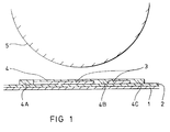
- a transfer according to the invention is illustrated diagrammatically by way of example in accompanying Figure 1.
- the transfer consists of a backing paper 1, release layer 2, design layer 3 and covercoat layer 4.
- the surface of a resilient transfer pad is shown at 5, in position above the transfer and ready to be brought into contact therewith to remove the design and covercoat layers from the backing paper.
- covercoat extends beyond the limits of the design layer to provide marginal portions 4A, 4B and 4C which are in contact with the release layer 2.
Claims (10)
- Übertragungsfolie zur Verwendung für das automatische Auflegen und umfassend ein Unterlagspapier, eine abziehbare Schicht, eine Musterschicht und eine Deckschicht, wobei die Schutzschicht gebildet wird aus einem in der Hitze aktivierbaren Adhäsiv und sich über eine Fläche erstreckt, die größer ist als die Musterschicht, und wobei die Musterschicht aus Druckfarbe gebildet wird, deren Medium hitzeaktivierbare adhäsive Eigenschaften hat.
- Übertragungsfolie nach Anspruch 1, wobei die Musterschicht keramisches Emaille umfaßt.
- Übertragungsfolie nach Anspruch 1 oder Anspruch 2, wobei die maximale Klebrigkeit der Deckschicht bzw. der Musterschichten bei verschiedenen Temperaturen erreicht wird.
- Übertragungsfolie nach Anspruch 1 oder Anspruch 2, wobei die Deckschicht ein Acryl- oder Zelluloseharz umfaßt.
- Übertragungsfolie nach Anspruch 1 oder Anspruch 2, wobei das Medium der Musterschicht ein Acrylharz umfaßt.
- Übertragungsfolie nach Anspruch 5, wobei das Harz ein Copolymer von Butylmethacrylat und Methylmethacrylat umfaßt und ein Molekulargewicht im Bereich von ungefähr 20 000 bis 30 000 hat.
- Übertragungsfolie nach einem der vorhergehenden Ansprüche, wobei die Musterschicht gebildet wird aus einer Druckfarbe, die ein Pigment oder ein anderes farbgebendes Material und Glasurmasse oder Glasfritten als Emaille und ein Medium enthält, wobei das Gewichtsverhältnis von Emaille zu Medium im Bereich von 250-300:100 zur Verzierung eines Glassubstrats oder 150-250:100 zur Verzierung eines Tongutmaterials beträgt.
- Verfahren zum automatischen Auflegen eines Musters auf die Oberfläche eines irdenen Gegenstandes unter Verwendung einer Übertragungsfolie, umfassend ein Unterlagspapier, eine abziehbare Schicht, eine Musterschicht und eine Deckschicht, wobei die Musterschicht aus Druckfarbe gebildet wird, deren Medium hitzeaktivierbare adhäsive Eigenschaften hat, die Deckschicht aus einem hitzeaktivierbaren Klebstoff gebildet wird und sich über eine Fläche erstreckt, die größer ist als die der Musterschicht, um am Rand freie Teile der Deckschicht zu liefern, wobei das Verfahren umfaßt, daß man die Übertragungsfolie auf eine erhitzte Platte aufbringt, um die abziehbare Wachsschicht zu schmelzen, ein erhitztes Druckkissen in Kontakt mit der Deckschicht bringt, um die adhäsiven Eigenschaften dieser Schicht zu aktivieren, das Druckkissen einschließlich der Deckschicht und der Musterschichten abzieht, das Kissen einschließlich dieser Schichten in Kontakt mit der Oberfläche eines irdenen Gegenstandes bringt und das Kissen abzieht, wobei der Adhäsionskoeffizient der Deckschicht bezüglich des Druckkissens geringer ist als der Akhäsionskoeffizient der Musterschicht und der Randteile der Deckschicht bezüglich des Gegenstandes, wodurch diese Schichten von dem Kissen auf den Gegenstand transferiert werden.
- Verfahren nach Anspruch 8, wobei die Platte auf eine Temperatur im Bereich von 70 bis 100°C erhitzt wird und das Druckkissen auf eine Temperatur im Bereich von 100 bis 130°C erhitzt wird.
- Verfahren nach Anspruch 8 oder Anspruch 9, wobei die Musterschicht keramisches Emaille umfaßt.
Applications Claiming Priority (2)
| Application Number | Priority Date | Filing Date | Title |
|---|---|---|---|
| GB878702063A GB8702063D0 (en) | 1987-01-30 | 1987-01-30 | Transfer for automatic application |
| GB8702063 | 1987-01-30 |
Publications (2)
| Publication Number | Publication Date |
|---|---|
| EP0276965A1 EP0276965A1 (de) | 1988-08-03 |
| EP0276965B1 true EP0276965B1 (de) | 1992-04-22 |
Family
ID=10611464
Family Applications (1)
| Application Number | Title | Priority Date | Filing Date |
|---|---|---|---|
| EP88300580A Expired - Lifetime EP0276965B1 (de) | 1987-01-30 | 1988-01-25 | Für automatisches Auflegen geeignete Übertragungsfolie |
Country Status (7)
| Country | Link |
|---|---|
| US (1) | US5069954A (de) |
| EP (1) | EP0276965B1 (de) |
| JP (1) | JPS63260499A (de) |
| KR (1) | KR880008889A (de) |
| CN (1) | CN1017790B (de) |
| DE (1) | DE3870267D1 (de) |
| GB (1) | GB8702063D0 (de) |
Families Citing this family (26)
| Publication number | Priority date | Publication date | Assignee | Title |
|---|---|---|---|---|
| GB2210828B (en) * | 1987-10-12 | 1991-09-11 | Josiah Wedgwood And Son Limite | Transfers and methods of decorating using same |
| WO1990005031A1 (en) * | 1988-11-07 | 1990-05-17 | Brandt Manufacturing Systems, Inc. | Glass container transparent coating system |
| GB2245847A (en) * | 1990-04-02 | 1992-01-15 | Federal Printers Limited | Stamping foil |
| US5411792A (en) * | 1992-02-27 | 1995-05-02 | Sumitomo Metal Mining Co., Ltd. | Transparent conductive substrate |
| ES2088347B1 (es) * | 1993-08-11 | 1998-01-01 | Ruiz Alayeto Maria Teresa | Procedimiento para la impresion de laminas transferibles a cualquier tipo de superficies |
| US5603259A (en) * | 1993-08-31 | 1997-02-18 | Crown Roll Leaf, Inc. | In-line cold foil transfer process and apparatus |
| US5830529A (en) * | 1996-01-11 | 1998-11-03 | Ross; Gregory E. | Perimeter coating alignment |
| US5976674A (en) * | 1996-04-19 | 1999-11-02 | Ngk Spark Plug, Co., Ltd. | Transfer sheet, a method of transferring a figuration therefrom and a ceramic product on which the figuration is printed |
| GB9820352D0 (en) | 1998-09-19 | 1998-11-11 | Polycarta Limited | Tranfers |
| EP0993968B1 (de) * | 1998-10-13 | 2003-01-15 | Bush Industries, Inc. | Verfahren zum Dekorieren eines Gegenstandes |
| DE59810916D1 (de) * | 1998-10-13 | 2004-04-08 | Bush Ind Inc | Verfahren zum farbigen Dekorieren eines Gegenstandes |
| DE59810918D1 (de) * | 1998-10-13 | 2004-04-08 | Bush Ind Inc | Verfahren zum Aufbringen eines Farbdekors auf ein Substrat |
| US6796733B2 (en) | 2000-10-31 | 2004-09-28 | International Imaging Materials Inc. | Thermal transfer ribbon with frosting ink layer |
| US7507453B2 (en) * | 2000-10-31 | 2009-03-24 | International Imaging Materials, Inc | Digital decoration and marking of glass and ceramic substrates |
| US6766734B2 (en) * | 2000-10-31 | 2004-07-27 | International Imaging Materials, Inc. | Transfer sheet for ceramic imaging |
| US6854386B2 (en) | 2000-10-31 | 2005-02-15 | International Imaging Materials Inc. | Ceramic decal assembly |
| US6990904B2 (en) | 2000-10-31 | 2006-01-31 | International Imaging Materials, Inc | Thermal transfer assembly for ceramic imaging |
| FI115392B (fi) * | 2001-06-01 | 2005-04-29 | Perlos Oyj | Menetelmä kolmiulotteisten pintojen kuviointiin |
| ES2575536T3 (es) * | 2003-10-07 | 2016-06-29 | Kao Corporation | Composición de tensioactivo |
| US20070218378A1 (en) * | 2006-03-15 | 2007-09-20 | Illinois Tool Works, Inc. | Thermally printable electrically conductive ribbon and method |
| WO2008021366A1 (en) * | 2006-08-11 | 2008-02-21 | Tohickon Corporation | Method and apparatus for pad printing of artificial glass eyes |
| US20090186554A1 (en) * | 2008-01-18 | 2009-07-23 | Tohickon Corporation | Pad printing with vitreous enamels |
| JP5374212B2 (ja) * | 2009-03-31 | 2013-12-25 | 株式会社ノリタケカンパニーリミテド | 窯変調転写紙および窯変調模様を有する陶磁器 |
| US10549521B2 (en) * | 2016-05-02 | 2020-02-04 | Benjamin S. Adner | Thermally controlled pad print ink transfer arrangement |
| CN106364203A (zh) * | 2016-08-30 | 2017-02-01 | 江阴市黄山船舶配件有限公司 | 船舶钢板配件的热转印工艺 |
| CN107187227A (zh) * | 2017-05-24 | 2017-09-22 | 昆山市生力包装印务有限公司 | 一种转移纸印刷工艺 |
Family Cites Families (12)
| Publication number | Priority date | Publication date | Assignee | Title |
|---|---|---|---|---|
| NL248143A (de) * | 1959-02-09 | |||
| US3445309A (en) * | 1966-05-04 | 1969-05-20 | Meyercord Co | Method of applying a vitreous decalcomania |
| US3967021A (en) * | 1971-04-30 | 1976-06-29 | Pictorial Productions, Inc. | Decalcomanias employed in offset transfer process |
| US4037008A (en) * | 1971-05-17 | 1977-07-19 | Photo-Lith International | Transfer printing process and article |
| DE2156542A1 (de) * | 1971-11-15 | 1973-05-24 | Kueppers Gerhard | Buntdruckbogen |
| US3886020A (en) * | 1972-08-17 | 1975-05-27 | Anchor Hocking Corp | Method of applying decals to surfaces of complex curvature |
| US4597815A (en) * | 1980-11-29 | 1986-07-01 | Nissha Printing Co., Ltd. | Transfer printing |
| JPS57135782A (en) * | 1981-02-10 | 1982-08-21 | Nissha Printing | Ceramic painting method |
| US4529624A (en) * | 1982-06-28 | 1985-07-16 | Dennison Manufacturing Co. | Discoloration resistant heat transfer labeling |
| JPS5911890A (ja) * | 1982-07-13 | 1984-01-21 | 三洋電機株式会社 | 洗濯機 |
| US4511425A (en) * | 1983-06-13 | 1985-04-16 | Dennison Manufacturing Company | Heated pad decorator |
| US4548857A (en) * | 1983-09-26 | 1985-10-22 | Dennison Manufacturing Co. | Heat transferable laminate |
-
1987
- 1987-01-30 GB GB878702063A patent/GB8702063D0/en active Pending
-
1988
- 1988-01-25 DE DE8888300580T patent/DE3870267D1/de not_active Expired - Lifetime
- 1988-01-25 EP EP88300580A patent/EP0276965B1/de not_active Expired - Lifetime
- 1988-01-28 US US07/149,355 patent/US5069954A/en not_active Expired - Fee Related
- 1988-01-29 KR KR1019880000779A patent/KR880008889A/ko not_active Application Discontinuation
- 1988-01-29 JP JP63017548A patent/JPS63260499A/ja active Pending
- 1988-01-30 CN CN88100545A patent/CN1017790B/zh not_active Expired
Also Published As
| Publication number | Publication date |
|---|---|
| US5069954A (en) | 1991-12-03 |
| JPS63260499A (ja) | 1988-10-27 |
| GB8702063D0 (en) | 1987-03-04 |
| CN88100545A (zh) | 1988-08-17 |
| KR880008889A (ko) | 1988-09-13 |
| CN1017790B (zh) | 1992-08-12 |
| DE3870267D1 (de) | 1992-05-27 |
| EP0276965A1 (de) | 1988-08-03 |
Similar Documents
| Publication | Publication Date | Title |
|---|---|---|
| EP0276965B1 (de) | Für automatisches Auflegen geeignete Übertragungsfolie | |
| US2970076A (en) | Vitreous decalcomania and method of decorating ceramic articles | |
| US3896249A (en) | Self-adhesive transfers | |
| US3007829A (en) | Vitreous decalcomania | |
| US4280939A (en) | Thermoplastic ink composition for decorating glass, glass-ceramic, and ceramic ware | |
| JPS5945000B2 (ja) | 熱剥離性デカルコマニア | |
| US4303717A (en) | Heat release layer for decalcomanias | |
| EP0055395B1 (de) | Übertragungsmaterial | |
| US3894167A (en) | Decalcomania for decorating ceramic ware | |
| US4117182A (en) | Heat release layer for decalcomanias | |
| US4261749A (en) | Thermoplastic inks suitable for pressure release-type decalcomania | |
| EP0312299B1 (de) | Übertragungsfolie und Verfahren zu ihrer Anwendung zum Dekorieren | |
| GB2085805A (en) | Printing medium for use with silicone transfer members | |
| US3967021A (en) | Decalcomanias employed in offset transfer process | |
| EP0057940A2 (de) | Transfermaterial und Verfahren zum Färben der Oberfläche eines Gegenstandes | |
| EP1640426A2 (de) | Hitzebeständiges Etikett | |
| US3887420A (en) | Offset transfer of decalcomanias | |
| JP2903547B2 (ja) | 陶磁器絵付け用転写シート | |
| US2520992A (en) | Screening paste | |
| JPH0249013B2 (de) | ||
| JP2899245B2 (ja) | 加熱転写マーク | |
| EP0244174A1 (de) | Heissübertragbare Offset-Transferfolie | |
| JP2000218997A (ja) | 低温焼き付け転写紙 | |
| JPS6280100A (ja) | ガラス質またはセラミツク質表面を有する基体への絵付け方法 | |
| KR100269773B1 (ko) | 열팽창 및 흡착을 이용한 다양한 문양의 전사방법 |
Legal Events
| Date | Code | Title | Description |
|---|---|---|---|
| PUAI | Public reference made under article 153(3) epc to a published international application that has entered the european phase |
Free format text: ORIGINAL CODE: 0009012 |
|
| AK | Designated contracting states |
Kind code of ref document: A1 Designated state(s): DE ES FR GB IT |
|
| 17P | Request for examination filed |
Effective date: 19890130 |
|
| RIN1 | Information on inventor provided before grant (corrected) |
Inventor name: SMITH, ROBERT W. Inventor name: COLE, DONALD |
|
| 17Q | First examination report despatched |
Effective date: 19901025 |
|
| GRAA | (expected) grant |
Free format text: ORIGINAL CODE: 0009210 |
|
| AK | Designated contracting states |
Kind code of ref document: B1 Designated state(s): DE ES FR GB IT |
|
| PG25 | Lapsed in a contracting state [announced via postgrant information from national office to epo] |
Ref country code: ES Free format text: THE PATENT HAS BEEN ANNULLED BY A DECISION OF A NATIONAL AUTHORITY Effective date: 19920422 Ref country code: IT Free format text: LAPSE BECAUSE OF FAILURE TO SUBMIT A TRANSLATION OF THE DESCRIPTION OR TO PAY THE FEE WITHIN THE PRE;WARNING: LAPSES OF ITALIAN PATENTS WITH EFFECTIVE DATE BEFORE 2007 MAY HAVE OCCURRED AT ANY TIME BEFORE 2007. THE CORRECT EFFECTIVE DATE MAY BE DIFFERENT FROM THE ONE RECORDED.SCRIBED TIME-LIMIT Effective date: 19920422 |
|
| REF | Corresponds to: |
Ref document number: 3870267 Country of ref document: DE Date of ref document: 19920527 |
|
| ET | Fr: translation filed | ||
| PLBE | No opposition filed within time limit |
Free format text: ORIGINAL CODE: 0009261 |
|
| STAA | Information on the status of an ep patent application or granted ep patent |
Free format text: STATUS: NO OPPOSITION FILED WITHIN TIME LIMIT |
|
| 26N | No opposition filed | ||
| PGFP | Annual fee paid to national office [announced via postgrant information from national office to epo] |
Ref country code: GB Payment date: 19971204 Year of fee payment: 11 |
|
| PGFP | Annual fee paid to national office [announced via postgrant information from national office to epo] |
Ref country code: FR Payment date: 19971218 Year of fee payment: 11 |
|
| PGFP | Annual fee paid to national office [announced via postgrant information from national office to epo] |
Ref country code: DE Payment date: 19971222 Year of fee payment: 11 |
|
| PG25 | Lapsed in a contracting state [announced via postgrant information from national office to epo] |
Ref country code: GB Free format text: LAPSE BECAUSE OF NON-PAYMENT OF DUE FEES Effective date: 19990125 |
|
| GBPC | Gb: european patent ceased through non-payment of renewal fee |
Effective date: 19990125 |
|
| PG25 | Lapsed in a contracting state [announced via postgrant information from national office to epo] |
Ref country code: FR Free format text: LAPSE BECAUSE OF NON-PAYMENT OF DUE FEES Effective date: 19990930 |
|
| PG25 | Lapsed in a contracting state [announced via postgrant information from national office to epo] |
Ref country code: DE Free format text: LAPSE BECAUSE OF NON-PAYMENT OF DUE FEES Effective date: 19991103 |
|
| REG | Reference to a national code |
Ref country code: FR Ref legal event code: ST |