EP0275093B2 - Entstörfilter mit verteilten Konstanten - Google Patents
Entstörfilter mit verteilten Konstanten Download PDFInfo
- Publication number
- EP0275093B2 EP0275093B2 EP88100395A EP88100395A EP0275093B2 EP 0275093 B2 EP0275093 B2 EP 0275093B2 EP 88100395 A EP88100395 A EP 88100395A EP 88100395 A EP88100395 A EP 88100395A EP 0275093 B2 EP0275093 B2 EP 0275093B2
- Authority
- EP
- European Patent Office
- Prior art keywords
- lead wire
- ground
- noise filter
- current carrying
- conductor
- Prior art date
- Legal status (The legal status is an assumption and is not a legal conclusion. Google has not performed a legal analysis and makes no representation as to the accuracy of the status listed.)
- Expired - Lifetime
Links
- WABPQHHGFIMREM-UHFFFAOYSA-N lead(0) Chemical compound [Pb] WABPQHHGFIMREM-UHFFFAOYSA-N 0.000 claims description 102
- 239000004020 conductor Substances 0.000 claims description 60
- 239000011888 foil Substances 0.000 claims description 5
- 238000004804 winding Methods 0.000 description 20
- 238000004519 manufacturing process Methods 0.000 description 8
- 238000002474 experimental method Methods 0.000 description 4
- 230000000694 effects Effects 0.000 description 3
- 239000000463 material Substances 0.000 description 3
- 239000004593 Epoxy Substances 0.000 description 2
- 229910052782 aluminium Inorganic materials 0.000 description 2
- XAGFODPZIPBFFR-UHFFFAOYSA-N aluminium Chemical compound [Al] XAGFODPZIPBFFR-UHFFFAOYSA-N 0.000 description 2
- 239000003990 capacitor Substances 0.000 description 2
- 230000008878 coupling Effects 0.000 description 2
- 238000010168 coupling process Methods 0.000 description 2
- 238000005859 coupling reaction Methods 0.000 description 2
- 230000007423 decrease Effects 0.000 description 2
- 230000001965 increasing effect Effects 0.000 description 2
- 238000005476 soldering Methods 0.000 description 2
- 229920002799 BoPET Polymers 0.000 description 1
- 239000011324 bead Substances 0.000 description 1
- 230000033228 biological regulation Effects 0.000 description 1
- 239000002131 composite material Substances 0.000 description 1
- 230000001939 inductive effect Effects 0.000 description 1
- 230000007257 malfunction Effects 0.000 description 1
- 229910052751 metal Inorganic materials 0.000 description 1
- 239000002184 metal Substances 0.000 description 1
- 238000000034 method Methods 0.000 description 1
- 238000003825 pressing Methods 0.000 description 1
- 239000011253 protective coating Substances 0.000 description 1
- 230000005855 radiation Effects 0.000 description 1
- 239000011347 resin Substances 0.000 description 1
- 229920005989 resin Polymers 0.000 description 1
- 238000000926 separation method Methods 0.000 description 1
- 230000001629 suppression Effects 0.000 description 1
- 230000001052 transient effect Effects 0.000 description 1
Images


Classifications
-
- H—ELECTRICITY
- H03—ELECTRONIC CIRCUITRY
- H03H—IMPEDANCE NETWORKS, e.g. RESONANT CIRCUITS; RESONATORS
- H03H9/00—Networks comprising electromechanical or electro-acoustic elements; Electromechanical resonators
- H03H9/46—Filters
-
- H—ELECTRICITY
- H01—ELECTRIC ELEMENTS
- H01G—CAPACITORS; CAPACITORS, RECTIFIERS, DETECTORS, SWITCHING DEVICES, LIGHT-SENSITIVE OR TEMPERATURE-SENSITIVE DEVICES OF THE ELECTROLYTIC TYPE
- H01G4/00—Fixed capacitors; Processes of their manufacture
- H01G4/40—Structural combinations of fixed capacitors with other electric elements, the structure mainly consisting of a capacitor, e.g. RC combinations
-
- H—ELECTRICITY
- H01—ELECTRIC ELEMENTS
- H01G—CAPACITORS; CAPACITORS, RECTIFIERS, DETECTORS, SWITCHING DEVICES, LIGHT-SENSITIVE OR TEMPERATURE-SENSITIVE DEVICES OF THE ELECTROLYTIC TYPE
- H01G4/00—Fixed capacitors; Processes of their manufacture
- H01G4/002—Details
- H01G4/228—Terminals
- H01G4/232—Terminals electrically connecting two or more layers of a stacked or rolled capacitor
-
- H—ELECTRICITY
- H03—ELECTRONIC CIRCUITRY
- H03H—IMPEDANCE NETWORKS, e.g. RESONANT CIRCUITS; RESONATORS
- H03H1/00—Constructional details of impedance networks whose electrical mode of operation is not specified or applicable to more than one type of network
- H03H1/0007—Constructional details of impedance networks whose electrical mode of operation is not specified or applicable to more than one type of network of radio frequency interference filters
-
- H—ELECTRICITY
- H03—ELECTRONIC CIRCUITRY
- H03H—IMPEDANCE NETWORKS, e.g. RESONANT CIRCUITS; RESONATORS
- H03H7/00—Multiple-port networks comprising only passive electrical elements as network components
- H03H7/01—Frequency selective two-port networks
- H03H7/09—Filters comprising mutual inductance
-
- H—ELECTRICITY
- H01—ELECTRIC ELEMENTS
- H01F—MAGNETS; INDUCTANCES; TRANSFORMERS; SELECTION OF MATERIALS FOR THEIR MAGNETIC PROPERTIES
- H01F17/00—Fixed inductances of the signal type
- H01F17/04—Fixed inductances of the signal type with magnetic core
- H01F17/06—Fixed inductances of the signal type with magnetic core with core substantially closed in itself, e.g. toroid
- H01F2017/065—Core mounted around conductor to absorb noise, e.g. EMI filter
-
- H—ELECTRICITY
- H01—ELECTRIC ELEMENTS
- H01F—MAGNETS; INDUCTANCES; TRANSFORMERS; SELECTION OF MATERIALS FOR THEIR MAGNETIC PROPERTIES
- H01F27/00—Details of transformers or inductances, in general
- H01F27/28—Coils; Windings; Conductive connections
- H01F27/2847—Sheets; Strips
-
- H—ELECTRICITY
- H01—ELECTRIC ELEMENTS
- H01F—MAGNETS; INDUCTANCES; TRANSFORMERS; SELECTION OF MATERIALS FOR THEIR MAGNETIC PROPERTIES
- H01F27/00—Details of transformers or inductances, in general
- H01F27/28—Coils; Windings; Conductive connections
- H01F27/32—Insulating of coils, windings, or parts thereof
- H01F27/323—Insulation between winding turns, between winding layers
-
- H—ELECTRICITY
- H03—ELECTRONIC CIRCUITRY
- H03H—IMPEDANCE NETWORKS, e.g. RESONANT CIRCUITS; RESONATORS
- H03H1/00—Constructional details of impedance networks whose electrical mode of operation is not specified or applicable to more than one type of network
- H03H2001/0021—Constructional details
- H03H2001/0042—Wound, ring or feed-through type capacitor
-
- H—ELECTRICITY
- H03—ELECTRONIC CIRCUITRY
- H03H—IMPEDANCE NETWORKS, e.g. RESONANT CIRCUITS; RESONATORS
- H03H1/00—Constructional details of impedance networks whose electrical mode of operation is not specified or applicable to more than one type of network
- H03H2001/0021—Constructional details
- H03H2001/005—Wound, ring or feed-through type inductor
-
- H—ELECTRICITY
- H03—ELECTRONIC CIRCUITRY
- H03H—IMPEDANCE NETWORKS, e.g. RESONANT CIRCUITS; RESONATORS
- H03H1/00—Constructional details of impedance networks whose electrical mode of operation is not specified or applicable to more than one type of network
- H03H2001/0092—Inductor filters, i.e. inductors whose parasitic capacitance is of relevance to consider it as filter
-
- Y—GENERAL TAGGING OF NEW TECHNOLOGICAL DEVELOPMENTS; GENERAL TAGGING OF CROSS-SECTIONAL TECHNOLOGIES SPANNING OVER SEVERAL SECTIONS OF THE IPC; TECHNICAL SUBJECTS COVERED BY FORMER USPC CROSS-REFERENCE ART COLLECTIONS [XRACs] AND DIGESTS
- Y10—TECHNICAL SUBJECTS COVERED BY FORMER USPC
- Y10T—TECHNICAL SUBJECTS COVERED BY FORMER US CLASSIFICATION
- Y10T29/00—Metal working
- Y10T29/43—Electric condenser making
- Y10T29/435—Solid dielectric type
Definitions
- the present invention relates generally to a noise filter, more specifically to a distributed constant type noise filter and a method of making such noise filter suited for DC power supply circuits or power circuits for analog or digital ICs (integrated circuits) or the like.
- Electronic circuits are normally designed to operate on a DC power supply voltage obtained from a battery or a utility AC power supply in conjunction with a rectifier circuit.
- DC-DC converters also known as switching type regulators
- Transient currents caused by switching or other electrical phenomena including load fluctuations due to switching operation of digital ICs or the like introduce noise of various frequency components into such power supply circuits. The noise may cause malfunctions or effects reducing the S/N ratio of other nearby electronic equipment or appliances through the supply line or electrical radiation.
- noise filters are used to protect or reduce such noise.
- regulations for noise reduction are becoming increasingly strict mainly because of an increasing circulation of a variety with high performances and sensitive electronic equipments.
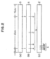
- Coupled near to both ends of the current carrying conductor 3 are lead wires 1 and 2. Also coupled near to one end of the ground conductor 5 is a ground lead wire 4.
- the inductance formed between both lead wires 1 and 2 depends on the number of turns and the length of the current carrying conductor 3.
- a certain large capacitance is developed between the current carrying conductor 3 and the ground conductor 5 because they are opposed to each other with the thin dielectric sheet 6 therebetween.
- An equivalent circuit of the resulting distributed constant type noise filter is illustrated in Fig. 7(C).
- Such distributed constant type noise filter is relatively simple and yet has relatively good attenuation characteristic over a wide frequency range. But no one has ever attempted to commercially make such noise filters. The primary reasons include the difficulty in making the connection of at least three load wires despite a required relatively small size resulting in a low production yield. Thus, noise filters of such type are unsuitable for quantity production because of unavoidable large differences in attenuation characteristics and lead wire misalignment.
- the DE-U 7 026 843 discloses an electrical device having inductive and capacitive properties, the device being comprised by at least two coils of a sheet material, respectively, and wound side by side in a spiral manner.
- the coils have input and output lead wires the distance of which in the plane of the sheet material is set so as to provide the desired inductance and capacitance values of the electrical device.
- the noise filter according to the present invention is constructed according to the features of the appended claim 1.
- a noise filter according to the present invention is constructed as to meet the following requirements:
- the winding shaft is chosen to be small enough (approximately 2 to 3 mm) and the distance between the first lead wire of the current carrying conductor and the ground lead wire of the ground conductor is selected in the range of approximately 1/4 to 3/4 turn, more preferably to 1/4 to 1/2 turn.
- the second lead wire of the current carrying conductor is on or near one of the extension lines including the central axis and the first or ground lead wire. In this manner, the distance between the first lead wire and the ground lead wire is substantially 2.5 % of the entire distance between the first and second lead wires when the current carrying conductor and the ground conductor are spread.
- the wound conductors and dielectric films are removed from the shaft and pressed into an oval shape in such direction that the three lead wires align in a substantially straight line.
- the winding may be coated with epoxy or other suitable resin.
- a first lead wire 1 of a current carrying conductor 3 is first placed around a shaft 12 of about 2 to 3 mm in diameter.
- a ground lead wire 4 of a ground conductor 5 is then placed at 1/4 to 1/2 rotary position or turn from the first lead wire 1.
- both of the current carrying conductor 3 and the ground conductor 5 of predetermined length are wound continuously and a second lead wire 2 of the current carrying conductor 3 comes in a position on or near the horizontal symmetry axis 14 coupling the first lead wire 1 and the center of the shaft 12.
- the end of the winding 10 is glued before removing the winding 10 from the shaft 12.
- the winding 10 is compressed perpendicular to the axis 14, thereby deforming the center space 12' of the shaft 12 as shown in Fig. 1(B), thereby bringing the lead wires 1, 2 and 4 in line with substantially increased space between two adjacent lead wires.
- the ground lead wire 4 may be placed about 1/4 turn ahead of the first lead wire 1 to provide for a symmetrical lead wire arrangement with respect to the axis 14.
- a finished noise filter comprises a generally oval winding portion 10' and three inline lead wires 1, 2 and 4 extending from one side of the winding portion 10'.
- the winding portion 10' may be placed in a casing made of a metal foil or provided with a protective coating of epoxy or other suitable material.
- the ground lead wire 4 is placed between the first and second lead wires 1 and 2 of the current carrying conductor 3.
- the first lead wire 1 and the ground lead wire 4 are shifted by about 1/4 turn, but it differs from the first embodiment, in that the second lead wire 2 is on the symmetry axis 14' including the ground lead wire 4. Since the winding is compressed perpendicular to the axis 14' as shown in Fig. 1(E), the three lead wires are arranged in line in the sequential order 4-1-2. Unlike the case shown in Fig. 1(D), the ground lead wire 4 may be placed ahead of the first lead wire 1 by about 1/4 turn to provide a symmetrical lead wire arrangement with respect to the axis 14'.
- Fig. 2 Shown in Fig. 2 are spread current carrying and ground conductors 3 and 5 to show how the relative position of the first and second lead wires 1 and 2 and the ground lead wire 4 effects performance or attenuation characteristics of the noise filter.
- aluminum foils of 60 cm length, 10 mm width and 50 ⁇ m thickness are used for the conductors 3 and 5 as shown in Fig. 2.
- a mylar tape of 12 mm width and 25 ⁇ m thickness is used for the dielectric sheets 6 (not shown in Fig. 2).
- a wire of 0.8 mm in diameter is used for the lead wires 1, 2 and 4.
- the first lead wire 1 is connected to the current carrying conductor 3 at 5 cm from the left end.
- the distance between the first and second lead wires 1 and 2 is chosen to be about 40 cm and the conductors are wound about 25 turns.
- the ground lead wire 4 of the ground conductor 5 is set to a position B shifted to the right by 2 cm from the first lead wire position A, the midpoint C between both lead wires 1 and 2 and position E, being substantially equal to the position of the second lead wire 2.
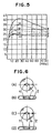
- Fig. 4 shows that attenuation reaches the maximum at a position B' where the ground lead wire 4 overlaps the first lead wire 1 and decreases as it departs from the first lead wire 1. Consequently, there is no appreciable difference in attenuation in which direction the ground lead wire 4 departs with respect to the first lead wire 1. That is, the ground lead wire may be ahead or lagged in winding procedure with respect to the first lead wire 4.
- foil type distributed constant noise filters to wind the current carrying conductor 3 and the ground conductor 5 around a sufficiently small diameter shaft 12 with the first lead wire 1 of the current carrying conductor 3 and the ground lead wire 4 of the ground conductor 5 shifted by about 1/4 to 1/2 turn, or about 1/4 to 3/4 turn in case of fairly large distance between the first lead wire 1 and the second lead wire 2.
- excellent attenuation is impossible for such noise filters having the first lead wire 1 and the ground lead wire 4 departing more than one turn even if their angular separation is 1/4 to 1/2 (or 3/4) of a complete rotation.
- the outer diameter of the winding section 10 of the noise filter is so large that shifting the ground lead wire 4 from the second lead wire 2 by, for example, 1/2 turn for in-line alignment of the three lead wires, may result in a considerably large percentage departure from the second lead wire, thereby causing significant drop in attenuation. Consequently, the noise filters shown in Fig. 1 are an optimum in respect to uniformity of electrical characteristics and suitability for mass production.
- the arrangement of the first lead wire 1, the second lead wire 2 and the ground lead wire 4 may be either as in Fig. 1(C) or as in Fig. 1(F) for a relatively low frequency range, whereas the arrangement of Fig. 1(C) having the ground lead wire 4 between the first lead wire 1 and the second lead wire 2 is preferable for higher frequency (100 MHz or higher) applications. It is assumed that high frequency components of the input signal tend to directly couple from the first lead wire 1 to the second lead wire 2 which are relatively close to each other. Also, it is more effective to use a wider ground conductor than the current carrying conductor.
- the first and second lead wires may be used as the signal input and output terminals or vice versa. However, the characteristic curve of Fig.
- FIG. 3(A) depicts the case where the first and second lead wires are used as input and output terminals, respectively.
- the characteristic curve of Fig. 3(E) represents the so-called choke-input type noise filter replacing the first and second lead wires from the capacitor-input type.
- the latter noise filter provides larger attenuation at relatively low frequencies of about 10 MHz, but the attenuation drops at a 30 to 50 MHz frequency range. It is suggested that a cascade connection of these two different noise filters provides a composite noise filter of excellent attenuation over a wide frequency range.
- the ground lead wire 4 and the first lead wire 1 may be separated by about 1/2 turn with the second lead wire 2 on the symmetry line coupling the ground lead wire 4 and the first lead wire 1 as shown in Figs. 6(A), (B) or (C), (D).
- the ground lead wire 4 is in the outer position while in the mid-position of the first and second lead wires for the embodiment of Figs. 6(C) and (D).
- the distance between the first lead wire 1 and the ground lead wire 4 is about 5 mm in the finished noise filter when winding around the shaft 12 having a diameter of 3 mm.
- noise filters are all normal mode using a single current carrying conductor and a single ground conductor
- this invention is applicable to common mode type noise filters using two pairs of current carrying and ground conductors.
- the first and ground lead wires of each pair of current carrying and ground conductors are shifted by about half turn with respect to the winding shaft.
- the ground conductor 5 may be divided into two or more sections rather than using a continuous or single piece as in the above described embodiments.
- a ground lead wire is connected to each ground conductor section.
- the use of divided ground conductor helps to increase the maximum attenuation. It is essential in this example to maintain the above mentioned relationship between the first lead wire 1 of the current carrying conductor 3 and the ground lead wire 4 of the ground conductor 5 for obtaining a uniform attenuation characteristic. That is, the first lead wire 1 and the ground lead wire of the first ground conductor section are positioned close enough to each other.
- a magnetic core may be inserted in the center of the winding or a magnetic conductor may be used as the current carrying or the ground conductor, respectively, in order to increase the inductance.
- the distributed constant type noise filter sets the first lead wire of the current carrying conductor and the ground lead wire of the ground conductor within one turn, more preferably 1/4 to 3/4 turn, and the second lead wire of the current carrying conductor on or near the symmetry axis including the center of the winding shaft and the first or the ground lead wire.
- the attenuation characteristic of the noise filter is well controlled within a certain predictable range and the three lead wires are positioned in a predetermined in-line arrangement, thereby enabling the manufacture of such noise filters in large quantity. Consequently, this invention overcomes problems associated with conventional noise filters including non-uniformity of the electrical characteristics and low production yield.
Landscapes
- Engineering & Computer Science (AREA)
- Power Engineering (AREA)
- Manufacturing & Machinery (AREA)
- Microelectronics & Electronic Packaging (AREA)
- Physics & Mathematics (AREA)
- Acoustics & Sound (AREA)
- Filters And Equalizers (AREA)
- Fixed Capacitors And Capacitor Manufacturing Machines (AREA)
- Coils Or Transformers For Communication (AREA)
Claims (1)
- Entstörfilter mit verteilten Konstanten, mit einem stromführenden Folienleiter (3) mit einem ersten und einem zweiten Anschlußdraht (1, 2) und einem Massefolienleiter (5) mit einem Masseanschlußdraht (4), wobei die beiden Leiter (3, 5) in im wesentlichen Rohrform mit dielektrischen Blättern (6) zwischen diesen gewickelt sind, dadurch gekennzeichnet, daß der Masseanschlußdraht (4) ausreichend dicht am ersten Anschlußdraht (1) angeschlossen ist, jedoch von diesem mit einer effektiven Entfernung zwischen dem Masseanschlußdraht und dem ersten Anschlußdraht getrennt, der im wesentlichen 2,5 % des Abstandes zwischen dem ersten und dem zweiten Anschlußdraht (1, 2) entspricht, wobei der erste, der zweite und der Masseanschlußdraht im wesentlichen in einer Linie zueinander angeordnet sind.
Applications Claiming Priority (3)
| Application Number | Priority Date | Filing Date | Title |
|---|---|---|---|
| JP4968/87 | 1987-01-14 | ||
| JP496887 | 1987-01-14 | ||
| JP62004968A JP2770278B2 (ja) | 1987-01-14 | 1987-01-14 | ノイズ・フイルタ及びその製造方法 |
Publications (4)
| Publication Number | Publication Date |
|---|---|
| EP0275093A2 EP0275093A2 (de) | 1988-07-20 |
| EP0275093A3 EP0275093A3 (en) | 1989-07-26 |
| EP0275093B1 EP0275093B1 (de) | 1992-06-17 |
| EP0275093B2 true EP0275093B2 (de) | 2000-06-21 |
Family
ID=11598390
Family Applications (1)
| Application Number | Title | Priority Date | Filing Date |
|---|---|---|---|
| EP88100395A Expired - Lifetime EP0275093B2 (de) | 1987-01-14 | 1988-01-13 | Entstörfilter mit verteilten Konstanten |
Country Status (5)
| Country | Link |
|---|---|
| US (3) | US4847575A (de) |
| EP (1) | EP0275093B2 (de) |
| JP (1) | JP2770278B2 (de) |
| KR (1) | KR900008362B1 (de) |
| DE (1) | DE3871961T3 (de) |
Families Citing this family (23)
| Publication number | Priority date | Publication date | Assignee | Title |
|---|---|---|---|---|
| DE3909528A1 (de) * | 1988-03-23 | 1989-10-12 | Murata Manufacturing Co | Stoerschutzfilter |
| JP2826320B2 (ja) | 1988-07-14 | 1998-11-18 | 毅 池田 | 3端子型ノイズフィルタおよびその製造方法 |
| JPH02174108A (ja) * | 1988-12-26 | 1990-07-05 | Murata Mfg Co Ltd | 3端子コンデンサ |
| JPH0346225U (de) * | 1989-09-12 | 1991-04-30 | ||
| JPH0348918U (de) * | 1989-09-20 | 1991-05-13 | ||
| US5200720A (en) * | 1990-11-27 | 1993-04-06 | Sam Hwa Capacitor Co., Ltd. | Emi bead core filter, process and apparatus thereof |
| US5448448A (en) * | 1991-06-10 | 1995-09-05 | Canon Kabushiki Kaisha | Aluminum electrolytic capacitor device |
| JPH09293628A (ja) * | 1996-04-17 | 1997-11-11 | J C C Eng Kk | コンデンサ及びその製造方法 |
| US6118072A (en) * | 1997-12-03 | 2000-09-12 | Teledyne Technologies Incorp. | Device having a flexible circuit disposed within a conductive tube and method of making same |
| RU2149484C1 (ru) * | 1998-12-24 | 2000-05-20 | Сомов Анатолий Михайлович | Каскад приемного устройства с разделением ортогональных поляризаций двух диапазонов частот |
| TW499793B (en) * | 2000-08-30 | 2002-08-21 | Nec Tokin Corp | Distributed constant type noise filter |
| US7541909B2 (en) | 2002-02-08 | 2009-06-02 | Metglas, Inc. | Filter circuit having an Fe-based core |
| KR100635699B1 (ko) * | 2002-07-31 | 2006-10-17 | 엔이씨 도낀 가부시끼가이샤 | 큰 직류 하에서도 발열이 적은 전송선로형 노이즈 필터 |
| US7148768B2 (en) | 2003-08-21 | 2006-12-12 | Hioki Denki Kabushiki Kaisha | Filter element |
| JP2005160058A (ja) * | 2003-11-05 | 2005-06-16 | Hioki Ee Corp | フィルタ素子 |
| JP4851126B2 (ja) * | 2004-06-30 | 2012-01-11 | 日置電機株式会社 | フィルタ素子 |
| JP2006148762A (ja) * | 2004-11-24 | 2006-06-08 | Hioki Ee Corp | フィルタ素子 |
| US7656236B2 (en) | 2007-05-15 | 2010-02-02 | Teledyne Wireless, Llc | Noise canceling technique for frequency synthesizer |
| US8179045B2 (en) | 2008-04-22 | 2012-05-15 | Teledyne Wireless, Llc | Slow wave structure having offset projections comprised of a metal-dielectric composite stack |
| US9202660B2 (en) | 2013-03-13 | 2015-12-01 | Teledyne Wireless, Llc | Asymmetrical slow wave structures to eliminate backward wave oscillations in wideband traveling wave tubes |
| US11831290B2 (en) | 2017-07-25 | 2023-11-28 | Wjlp Company Inc. | Inductive-capacitive filters and associated systems and methods |
| US11183985B2 (en) | 2017-07-25 | 2021-11-23 | Wjlp Company Inc. | Inductive-capacitive filters and associated systems and methods |
| US11114232B2 (en) * | 2017-09-12 | 2021-09-07 | Raycap IP Development Ltd | Inductor assemblies |
Family Cites Families (18)
| Publication number | Priority date | Publication date | Assignee | Title |
|---|---|---|---|---|
| US2000441A (en) * | 1934-07-06 | 1935-05-07 | Bell Telephone Labor Inc | Filter |
| US2260296A (en) * | 1939-09-29 | 1941-10-28 | Bell Telephone Labor Inc | Electrical filter |
| US2884605A (en) * | 1953-09-11 | 1959-04-28 | Cornell Dubilier Electric | Electrical suppressor |
| GB934890A (en) * | 1961-02-24 | 1963-08-21 | Telephone Mfg Co Ltd | Improvements in and relating to electric supply systems and apparatus |
| US3365632A (en) * | 1966-06-14 | 1968-01-23 | Gen Electric | Wound capacitor |
| GB1220083A (en) * | 1967-03-28 | 1971-01-20 | Erie Technological Prod Ltd | Improvements in or relating to electrical capacitors |
| US4048593A (en) * | 1974-05-13 | 1977-09-13 | Zillman Jack H | Electrical component for providing integrated inductive-capacitive networks |
| JPS5212914U (de) * | 1975-07-16 | 1977-01-29 | ||
| JPS53106452A (en) * | 1977-02-28 | 1978-09-16 | Fujitsu Ltd | Method of making capacitor |
| SE7702537L (sv) * | 1977-03-07 | 1978-09-08 | Aga Ab | Forfarande och anordning for att rengora en lutande eller vertikal yta pa ett optiskt element |
| FR2383553A1 (fr) * | 1977-03-09 | 1978-10-06 | Siemens Sa | Nouveau composant electronique susceptible de constituer au moins un filtre |
| JPS53164647U (de) * | 1977-05-31 | 1978-12-23 | ||
| JPS5483736A (en) | 1977-12-16 | 1979-07-04 | Matsushita Electric Ind Co Ltd | Noise filter |
| JPS55148105A (en) * | 1979-05-08 | 1980-11-18 | Matsushita Electric Works Ltd | Preparation of aggregate material |
| JPS5775416A (en) * | 1980-10-29 | 1982-05-12 | Fujitsu Ltd | Method of wound type condenser |
| JPS6027212A (ja) * | 1983-07-25 | 1985-02-12 | Takeshi Ikeda | ノイズ・フイルタ |
| KR900007925B1 (ko) * | 1983-05-18 | 1990-10-23 | 다게시 이게다 | 노이즈 필터 |
| JPS60174416A (ja) * | 1984-02-20 | 1985-09-07 | Nakajima Doukoushiyo:Kk | 熱風加工器 |
-
1987
- 1987-01-14 JP JP62004968A patent/JP2770278B2/ja not_active Expired - Lifetime
- 1987-12-28 KR KR1019870015011A patent/KR900008362B1/ko not_active Expired
-
1988
- 1988-01-06 US US07/141,321 patent/US4847575A/en not_active Expired - Lifetime
- 1988-01-13 DE DE3871961T patent/DE3871961T3/de not_active Expired - Fee Related
- 1988-01-13 EP EP88100395A patent/EP0275093B2/de not_active Expired - Lifetime
- 1988-09-06 US US07/240,719 patent/US4870729A/en not_active Expired - Lifetime
-
1989
- 1989-08-18 US US07/395,499 patent/US5030933A/en not_active Expired - Lifetime
Also Published As
| Publication number | Publication date |
|---|---|
| US4870729A (en) | 1989-10-03 |
| DE3871961T3 (de) | 2000-12-07 |
| EP0275093B1 (de) | 1992-06-17 |
| DE3871961D1 (de) | 1992-07-23 |
| DE3871961T2 (de) | 1992-12-03 |
| US4847575A (en) | 1989-07-11 |
| EP0275093A3 (en) | 1989-07-26 |
| US5030933A (en) | 1991-07-09 |
| JPS63174416A (ja) | 1988-07-18 |
| EP0275093A2 (de) | 1988-07-20 |
| JP2770278B2 (ja) | 1998-06-25 |
| KR880009480A (ko) | 1988-09-15 |
| KR900008362B1 (ko) | 1990-11-17 |
Similar Documents
| Publication | Publication Date | Title |
|---|---|---|
| EP0275093B2 (de) | Entstörfilter mit verteilten Konstanten | |
| US5206621A (en) | Barrel-wound conductive film transformer | |
| US5481792A (en) | Inductor winding method | |
| US20020149461A1 (en) | Apparatus and method for PCB winding planar magnetic devices | |
| US4922156A (en) | Integrated power capacitor and inductors/transformers utilizing insulated amorphous metal ribbon | |
| US3911332A (en) | Wound transformers and machine for making the same | |
| JP2826320B2 (ja) | 3端子型ノイズフィルタおよびその製造方法 | |
| JPH04337610A (ja) | インダクタンス部品 | |
| JP2728439B2 (ja) | 4端子型ノイズフィルタおよびその製造方法 | |
| JPH10308315A (ja) | インダクタンス要素部品 | |
| US4866407A (en) | Noise filter and method of making the same | |
| US4904973A (en) | Foil-roll electronic part | |
| JPH03259608A (ja) | Lcノイズフィルタ | |
| EP0276684B1 (de) | Elektronisches Bauelement mit Rollenfolie und sein Herstellungsverfahren | |
| HK1006338B (en) | Noise filter and method of making the same | |
| EP0126446B1 (de) | Entstörfilter und Verfahren zu seiner Herstellung | |
| JPH05291865A (ja) | Lcフィルタ | |
| JPS61134003A (ja) | コイル | |
| US4908934A (en) | Process of producing a foil-roll electronic part | |
| JP2005160058A (ja) | フィルタ素子 | |
| JP3306092B2 (ja) | ノイズ・フィルタ | |
| JPH05217770A (ja) | トランス装置 | |
| US4320373A (en) | Power transformer with high coupling coefficient | |
| KR960015676B1 (ko) | 4단자형 노이즈필터 및 그 제조방법 | |
| JPH01289228A (ja) | ノイズフィルタ |
Legal Events
| Date | Code | Title | Description |
|---|---|---|---|
| PUAI | Public reference made under article 153(3) epc to a published international application that has entered the european phase |
Free format text: ORIGINAL CODE: 0009012 |
|
| AK | Designated contracting states |
Kind code of ref document: A2 Designated state(s): DE FR GB NL |
|
| PUAL | Search report despatched |
Free format text: ORIGINAL CODE: 0009013 |
|
| AK | Designated contracting states |
Kind code of ref document: A3 Designated state(s): DE FR GB NL |
|
| 17P | Request for examination filed |
Effective date: 19890731 |
|
| 17Q | First examination report despatched |
Effective date: 19910927 |
|
| GRAA | (expected) grant |
Free format text: ORIGINAL CODE: 0009210 |
|
| AK | Designated contracting states |
Kind code of ref document: B1 Designated state(s): DE FR GB NL |
|
| REF | Corresponds to: |
Ref document number: 3871961 Country of ref document: DE Date of ref document: 19920723 |
|
| ET | Fr: translation filed | ||
| PLBI | Opposition filed |
Free format text: ORIGINAL CODE: 0009260 |
|
| 26 | Opposition filed |
Opponent name: SIEMENS AKTIENGESELLSCHAFT, BERLIN UND MUENCHEN Effective date: 19930317 |
|
| NLR1 | Nl: opposition has been filed with the epo |
Opponent name: SIEMENS AG. |
|
| PLAW | Interlocutory decision in opposition |
Free format text: ORIGINAL CODE: EPIDOS IDOP |
|
| APAC | Appeal dossier modified |
Free format text: ORIGINAL CODE: EPIDOS NOAPO |
|
| APAE | Appeal reference modified |
Free format text: ORIGINAL CODE: EPIDOS REFNO |
|
| APAC | Appeal dossier modified |
Free format text: ORIGINAL CODE: EPIDOS NOAPO |
|
| PLAW | Interlocutory decision in opposition |
Free format text: ORIGINAL CODE: EPIDOS IDOP |
|
| PUAH | Patent maintained in amended form |
Free format text: ORIGINAL CODE: 0009272 |
|
| STAA | Information on the status of an ep patent application or granted ep patent |
Free format text: STATUS: PATENT MAINTAINED AS AMENDED |
|
| 27A | Patent maintained in amended form |
Effective date: 20000621 |
|
| AK | Designated contracting states |
Kind code of ref document: B2 Designated state(s): DE FR GB NL |
|
| NLR2 | Nl: decision of opposition | ||
| ET3 | Fr: translation filed ** decision concerning opposition | ||
| NLR3 | Nl: receipt of modified translations in the netherlands language after an opposition procedure | ||
| REG | Reference to a national code |
Ref country code: GB Ref legal event code: IF02 |
|
| APAH | Appeal reference modified |
Free format text: ORIGINAL CODE: EPIDOSCREFNO |
|
| PGFP | Annual fee paid to national office [announced via postgrant information from national office to epo] |
Ref country code: NL Payment date: 20060119 Year of fee payment: 19 Ref country code: FR Payment date: 20060119 Year of fee payment: 19 |
|
| PGFP | Annual fee paid to national office [announced via postgrant information from national office to epo] |
Ref country code: GB Payment date: 20060123 Year of fee payment: 19 |
|
| PGFP | Annual fee paid to national office [announced via postgrant information from national office to epo] |
Ref country code: DE Payment date: 20060125 Year of fee payment: 19 |
|
| PG25 | Lapsed in a contracting state [announced via postgrant information from national office to epo] |
Ref country code: DE Free format text: LAPSE BECAUSE OF NON-PAYMENT OF DUE FEES Effective date: 20070801 |
|
| GBPC | Gb: european patent ceased through non-payment of renewal fee |
Effective date: 20070113 |
|
| NLV4 | Nl: lapsed or anulled due to non-payment of the annual fee |
Effective date: 20070801 |
|
| REG | Reference to a national code |
Ref country code: FR Ref legal event code: ST Effective date: 20070930 |
|
| PG25 | Lapsed in a contracting state [announced via postgrant information from national office to epo] |
Ref country code: GB Free format text: LAPSE BECAUSE OF NON-PAYMENT OF DUE FEES Effective date: 20070113 |
|
| PG25 | Lapsed in a contracting state [announced via postgrant information from national office to epo] |
Ref country code: NL Free format text: LAPSE BECAUSE OF NON-PAYMENT OF DUE FEES Effective date: 20070801 |
|
| PG25 | Lapsed in a contracting state [announced via postgrant information from national office to epo] |
Ref country code: FR Free format text: LAPSE BECAUSE OF NON-PAYMENT OF DUE FEES Effective date: 20070131 |