EP0273715A2 - Procédé de fabrication d'un dispositif semi-conducteur par déposition d'une couche métallique - Google Patents
Procédé de fabrication d'un dispositif semi-conducteur par déposition d'une couche métallique Download PDFInfo
- Publication number
- EP0273715A2 EP0273715A2 EP87311389A EP87311389A EP0273715A2 EP 0273715 A2 EP0273715 A2 EP 0273715A2 EP 87311389 A EP87311389 A EP 87311389A EP 87311389 A EP87311389 A EP 87311389A EP 0273715 A2 EP0273715 A2 EP 0273715A2
- Authority
- EP
- European Patent Office
- Prior art keywords
- wafer
- layer
- aluminium
- metal layer
- temperature
- Prior art date
- Legal status (The legal status is an assumption and is not a legal conclusion. Google has not performed a legal analysis and makes no representation as to the accuracy of the status listed.)
- Granted
Links
- 238000000034 method Methods 0.000 title claims abstract description 39
- 229910052751 metal Inorganic materials 0.000 title claims abstract description 19
- 239000002184 metal Substances 0.000 title claims abstract description 19
- 239000004065 semiconductor Substances 0.000 title claims description 15
- 238000004544 sputter deposition Methods 0.000 claims abstract description 20
- 229910045601 alloy Inorganic materials 0.000 claims abstract description 18
- 239000000956 alloy Substances 0.000 claims abstract description 18
- 238000009413 insulation Methods 0.000 claims abstract description 17
- 229910052782 aluminium Inorganic materials 0.000 claims abstract description 15
- 239000004411 aluminium Substances 0.000 claims abstract description 13
- XAGFODPZIPBFFR-UHFFFAOYSA-N aluminium Chemical compound [Al] XAGFODPZIPBFFR-UHFFFAOYSA-N 0.000 claims abstract description 13
- 239000006104 solid solution Substances 0.000 claims abstract description 12
- 238000000151 deposition Methods 0.000 claims abstract description 10
- 229910052710 silicon Inorganic materials 0.000 claims abstract description 8
- 229910000838 Al alloy Inorganic materials 0.000 claims abstract description 5
- 239000010703 silicon Substances 0.000 claims abstract description 3
- 229910002056 binary alloy Inorganic materials 0.000 claims description 4
- 230000008021 deposition Effects 0.000 claims description 2
- AZDRQVAHHNSJOQ-UHFFFAOYSA-N alumane Chemical group [AlH3] AZDRQVAHHNSJOQ-UHFFFAOYSA-N 0.000 claims 1
- 239000000203 mixture Substances 0.000 claims 1
- 238000000059 patterning Methods 0.000 abstract description 6
- 230000006866 deterioration Effects 0.000 abstract description 5
- XUIMIQQOPSSXEZ-UHFFFAOYSA-N Silicon Chemical compound [Si] XUIMIQQOPSSXEZ-UHFFFAOYSA-N 0.000 abstract description 2
- 230000015572 biosynthetic process Effects 0.000 abstract description 2
- 238000005137 deposition process Methods 0.000 abstract description 2
- 230000002265 prevention Effects 0.000 abstract 1
- 239000010410 layer Substances 0.000 description 57
- 238000010438 heat treatment Methods 0.000 description 9
- 239000010949 copper Substances 0.000 description 7
- VYPSYNLAJGMNEJ-UHFFFAOYSA-N Silicium dioxide Chemical compound O=[Si]=O VYPSYNLAJGMNEJ-UHFFFAOYSA-N 0.000 description 6
- 229910052802 copper Inorganic materials 0.000 description 6
- 239000002244 precipitate Substances 0.000 description 6
- 238000010276 construction Methods 0.000 description 5
- 239000007789 gas Substances 0.000 description 5
- 239000002365 multiple layer Substances 0.000 description 4
- 239000007787 solid Substances 0.000 description 4
- 230000002411 adverse Effects 0.000 description 3
- 238000001312 dry etching Methods 0.000 description 3
- 230000000694 effects Effects 0.000 description 3
- 230000010354 integration Effects 0.000 description 3
- 238000001556 precipitation Methods 0.000 description 3
- 235000012239 silicon dioxide Nutrition 0.000 description 3
- 239000000377 silicon dioxide Substances 0.000 description 3
- XKRFYHLGVUSROY-UHFFFAOYSA-N Argon Chemical compound [Ar] XKRFYHLGVUSROY-UHFFFAOYSA-N 0.000 description 2
- RYGMFSIKBFXOCR-UHFFFAOYSA-N Copper Chemical compound [Cu] RYGMFSIKBFXOCR-UHFFFAOYSA-N 0.000 description 2
- -1 and the like Substances 0.000 description 2
- 239000011362 coarse particle Substances 0.000 description 2
- 230000000875 corresponding effect Effects 0.000 description 2
- 238000010586 diagram Methods 0.000 description 2
- 239000000463 material Substances 0.000 description 2
- 239000011159 matrix material Substances 0.000 description 2
- 239000005360 phosphosilicate glass Substances 0.000 description 2
- 230000001105 regulatory effect Effects 0.000 description 2
- 239000000758 substrate Substances 0.000 description 2
- 239000010936 titanium Substances 0.000 description 2
- 229910021364 Al-Si alloy Inorganic materials 0.000 description 1
- RTAQQCXQSZGOHL-UHFFFAOYSA-N Titanium Chemical compound [Ti] RTAQQCXQSZGOHL-UHFFFAOYSA-N 0.000 description 1
- 229910052786 argon Inorganic materials 0.000 description 1
- 230000010485 coping Effects 0.000 description 1
- 238000004090 dissolution Methods 0.000 description 1
- 238000009429 electrical wiring Methods 0.000 description 1
- 230000008014 freezing Effects 0.000 description 1
- 238000007710 freezing Methods 0.000 description 1
- 230000005012 migration Effects 0.000 description 1
- 238000013508 migration Methods 0.000 description 1
- 239000002245 particle Substances 0.000 description 1
- 239000007790 solid phase Substances 0.000 description 1
- 229910052719 titanium Inorganic materials 0.000 description 1
Images


Classifications
-
- H—ELECTRICITY
- H01—ELECTRIC ELEMENTS
- H01L—SEMICONDUCTOR DEVICES NOT COVERED BY CLASS H10
- H01L21/00—Processes or apparatus adapted for the manufacture or treatment of semiconductor or solid state devices or of parts thereof
- H01L21/02—Manufacture or treatment of semiconductor devices or of parts thereof
- H01L21/04—Manufacture or treatment of semiconductor devices or of parts thereof the devices having potential barriers, e.g. a PN junction, depletion layer or carrier concentration layer
- H01L21/18—Manufacture or treatment of semiconductor devices or of parts thereof the devices having potential barriers, e.g. a PN junction, depletion layer or carrier concentration layer the devices having semiconductor bodies comprising elements of Group IV of the Periodic Table or AIIIBV compounds with or without impurities, e.g. doping materials
- H01L21/28—Manufacture of electrodes on semiconductor bodies using processes or apparatus not provided for in groups H01L21/20 - H01L21/268
- H01L21/283—Deposition of conductive or insulating materials for electrodes conducting electric current
-
- H—ELECTRICITY
- H01—ELECTRIC ELEMENTS
- H01L—SEMICONDUCTOR DEVICES NOT COVERED BY CLASS H10
- H01L21/00—Processes or apparatus adapted for the manufacture or treatment of semiconductor or solid state devices or of parts thereof
- H01L21/02—Manufacture or treatment of semiconductor devices or of parts thereof
- H01L21/04—Manufacture or treatment of semiconductor devices or of parts thereof the devices having potential barriers, e.g. a PN junction, depletion layer or carrier concentration layer
- H01L21/18—Manufacture or treatment of semiconductor devices or of parts thereof the devices having potential barriers, e.g. a PN junction, depletion layer or carrier concentration layer the devices having semiconductor bodies comprising elements of Group IV of the Periodic Table or AIIIBV compounds with or without impurities, e.g. doping materials
- H01L21/30—Treatment of semiconductor bodies using processes or apparatus not provided for in groups H01L21/20 - H01L21/26
- H01L21/31—Treatment of semiconductor bodies using processes or apparatus not provided for in groups H01L21/20 - H01L21/26 to form insulating layers thereon, e.g. for masking or by using photolithographic techniques; After treatment of these layers; Selection of materials for these layers
- H01L21/3205—Deposition of non-insulating-, e.g. conductive- or resistive-, layers on insulating layers; After-treatment of these layers
- H01L21/32051—Deposition of metallic or metal-silicide layers
Definitions
- the present invention relates to a technique for forming a metal layer and, more particularly, to a method for forming a metal layer by depositing aluminium (Al)-based alloy on a wafer by sputtering, and a semiconductor device formed by using that method.
- the metal layer forming technique according to the present invention can be widely used in the process of forming an electrical wiring for an integrated circuit (IC) or a large scale integration (LSI).
- IC integrated circuit
- LSI large scale integration
- an Al or Al-based alloy such as Al-1% by weight of silicon (Si), Al-2% by weight of copper (Cu), Al-1% by weight of Si-0.5% by weight of Cu, Al-1% by weight of Si-0.1% by weight of titanium (Ti), and the like are employed as the wiring materials for LSI's, since such alloys contribute to a decrease in the power dissipation, due to the low resistance thereof.
- the wiring layers using these alloys are usually formed by sputtering. Further, recent trends toward a higher integration and higher density of a semiconductor device, have led to the formation of a very steep step portion of a layer on which an Al wiring layer is formed.
- the ratio of the step height thereof to the width of the holes thereof is great. Accordingly, it is difficult to form an Al wiring layer having a good step coverage, i.e., a satisfactory degree of thickness, conforming to the shape of a layer thereunder.
- a technique is known of piling a plurality of Al wiring layers as a multiple layer stack, development an even higher integration and higher density of a device.
- a problem arises in that, if the step coverage of an Al wiring layer is not good, an adverse influence is exerted upon the step coverage of an insulation layer to be formed thereupon and, furthermore, this adverse influence is extended to the step coverage of another Al wiring layer to be formed thereon, and thus it is difficult to obtain a multiple-layer wiring construction having a good shape.
- One proposed technique therefore, comprises forming an insulation layer having at least one step portion on the wafer; and forming said metal layer by depositing the aluminium-based alloy over the insulation layer while the wafer is heated. According to this method, since the surface of the wafer is heated, Al atoms deposited on the wafer can be easily moved on the surface thereof after the deposition process is completed, and as a result, the step coverage of the layer at the step portion can be improved. However, if the temperature of the wafer is too high, another problem arises as follows.
- an admixture contained in the Al-based alloy e.g., atoms of Si, Cu, and the like, precipitates in the vicinity of the interface between the Al wiring layer and the layer thereunder, e.g., a semiconductor layer, to such an extent that this precipitated admixture cannot be completely removed in a later process. Accordingly, this causes difficulties in, for example, a patterning of the Al wiring layer at the later stage, because it is technically difficult to remove both an unnecessary Al metal portion and the precipitated admixture such as Si, even if the patterning process is carried out by dry etching.
- the wafer is heated to a temperature higher than the temperature at which a solid solution is formed in the aluminium-based alloy.
- This technique provides a metal layer forming method which realizes a good step coverage at a step portion to make the surface of an Al alloy layer substantially flat, while preventing a deterioration in the quality of the layer and so facilitating a subsequent patterning step based on a subsequent dry etching process.
- Figure 1 shows a sectional view of an example of the step coverage in the construction of a typical Al multiple-layer wiring.
- the construction is formed by sequentially depositing, on a semiconductor layer or substrate 11, a first insulation layer 12 of silicon dioxide (SiO2), a first wiring layer 13 of Al, a second insulation layer 14 of phosphosilicate glass (PSG), and a second wiring layer 15 of Al.
- SiO2 silicon dioxide
- PSG phosphosilicate glass
- the coverage of the second Al wiring layer 15 is relatively poor.
- the connection of the second Al wiring layer 15 is very unsatisfactory because of the thinness of the layer 15 at the portions adjacent to the contact holes, i.e., the thin portion of the layer 15 is easily broken due to a migration of Al atoms over a long period of time, and thus the operational reliability of an LSI device is reduced.
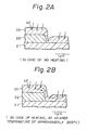
- Figure 2A shows a sectional view of an example of the step coverage when heating is not carried out.
- reference 21 denotes a semiconductor layer or substrate
- reference 22 denotes an insulation layer of, e.g., SiO2
- reference 23 denotes an Al wiring layer.
- the construction shown in Fig. 2A is part of a device formed on a wafer (not shown). As shown in Fig. 2A, where the heating is not applied to the wafer, little movement of the Al atoms deposited on the wafer occurs, and accordingly, the Al atoms remain in the positions at which they are deposited. As a result, the step coverage at the step portion becomes relatively poor.
- Fig. 2B which shows a sectional view of an example of the step coverage where the temperature of a heater (not shown) for heating the wafer is set at approximately 200°C
- the shape of the Al wiring layer 23 at the step portion is improved. That is, when heating is applied to the wafer, Al atoms deposited on the wafer can be easily moved toward the step portion, as shown by arrow marks, and accordingly, collected in the step portion. As a result, the step coverage at the step portion becomes better than that of Fig. 2A.
- an admixture contained in the Al-based alloy e.g., atoms of Si, Cu, and the like, precipitates in the vicinity of the interface between the Al wiring layer 23 and the semiconductor layer 21.
- the amount of atoms precipitated near the interface at the heater temperature of approximately 200°C is within a permissible amount, i.e., at which the precipitated atoms of Si, Cu, and the like can be completely removed during a patterning process carried out at a later stage. Therefore, in this case (Fig. 2B), no problem arises with respect to the precipitation of the admixture.
- Figure 3 shows a sectional view of an example of step coverage when the temperature of the heater is set at approximately 400°C.
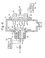
- Figure 4 illustrates a constitution of the sputtering apparatus for implementing the metal layer forming method according to the present invention.
- reference 41 denotes a vacuum container having an opening at one side
- a heater block 42 is held by a block holding member 43 fixed to the container 41 by screws.
- the heater block 42 is formed of copper, which has a good thermal conductivity, and a thermocouple 44 and eight annularly arranged cartridge type heaters 45 are embedded therein.
- Reference 46 denotes a heater controller, which regulates the temperatures of each of the cartridge heaters 45 to a constant temperature, in accordance with the temperature of the heater block 42 detected by the thermocouple 44.
- the constant temperature is set at 600°C.
- the heater block 42 has a through hole in the central portion thereof, and argon (Ar) gas supplied from an external source is introduced, via a flow regulating valve 47, through the through hole of the block 42 into the vacuum container 41.
- Reference 48 denotes a semiconductor wafer, which is held by a pair of holding members 50 mounted on a corresponding tray 49 and arranged at a predetermined position, i.e., opposite to the end face, of the heater block 42, from which Ar gas is delivered.
- the arrangement of the wafer 48 is performed by a carrying system (not shown).
- a target 51 consisting of binary alloy of Al-1%Si is provided in an opening at the side of the vacuum container opposite to the wafer 48.
- the target 51 is held via an insulation member 52 by a target holding member 53, which is fixed to the vacuum container 41 by screws, and as a result, the opening is sealed.
- the target 51 is connected to a direct current (DC) power source 54 having a voltage of -400 to -500 V, a current of 15 to 20 A, and a power of 7 to 10 kW, and the holding member 53 is grounded commonly with the vacuum container 41.
- DC direct current
- Reference 55 denotes a magnet, which forms an annular magnetic field area for confining electrons in the vicinity of the surface of the target 51.
- Reference 56 denotes a motor for rotating the magnet 55 so that the magnitude of the magnetic field is made uniform over the whole surface of the target.
- the operation of the magnet 55 causes the surface of the target 51 to be biased to a high negative potential and, accordingly, a high density plasma state is realized, resulting in an improvement in the speed of the forming of a layer.
- Reference 57 denotes a conductance regulating valve, which regulates the gas pressure within the vacuum container 41 to a predetermined value. Gas within the container is evacuated with cryopump (not shown) through the valve 57.
- the sputtering apparatus shown in Fig. 4 does not feature the present invention, and therefore a detailed explanation of the operation thereof will be omitted.
- the wafer 48 is heated by the heater block 42, i.e., concretely, heated by thermal contact with the Ar gas introduced via the through hole of the block 42.
- the material of the target 51 i.e., Al-1%Si
- the temperature of the wafer 48 rises.
- the rise of the temperature of the wafer 48 depends upon both the temperature produced by the heat from the heater block 42 and that produced by the heat due to the deposition of atoms.
- the heater temperature is set at approximately 600°C, the measured values of the temperature of the wafer 48 are indicated in the following table.
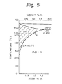
- Figure 5 is a graph illustrating an equilibrium diagram of the binary alloy (Al-Si) with respect to the temperature.
- the hatched region indicated by reference P represents a solid solution region, in which Si atoms are brought to the state of a solid solution in the Al matrix.
- Si atoms precipitates in the Al matrix.
- the state of the Al-Si alloy changes at approximately 525°C. That is, an admixture of Si is deposited in the Al solid at a temperature lower than 525°C, but it is brought to the state of an absolutely solid solution in the Al solid at a temperature higher than 525°C.
- the temperature of the wafer during the sputtering process rises from the time that the sputtering is started, i.e., the state (460°C) in CASE-2 to the state (570°C) in CASE-4. Therefore, Si atoms in the films deposited on the wafer are brought to the state of an absolutely solid solution in the Al solid.
- Figure 6 illustrates an example of the step coverage obtained when Si atoms are brought to the state of a solid solution. Comparing the sectional view at the heater temperature of approximately 600°C in Fig. 6 with that at the heater temperature of approximately 400°C in Fig. 3, representing a conventional example, it will be appreciated that the shape of the Al wiring layer 63 at the step portion in Fig. 6 is flatter than the corresponding shape in Fig.
- the shape of the layer at the step portion can be planarized, and since the admixture does not precipitate in the form of coarse particles in the vicinity of the interface, a patterning process based on a subsequent dry etching can be facilitated. Also, the surface of the Al wiring layer formed at the step portion is relatively smooth. Furthermore, the Al wiring layer is stable with respect to a subsequent heating process at 450°C to 500°C and thus a deterioration in the quality of the layer can be prevented.
Landscapes
- Engineering & Computer Science (AREA)
- Physics & Mathematics (AREA)
- Condensed Matter Physics & Semiconductors (AREA)
- General Physics & Mathematics (AREA)
- Manufacturing & Machinery (AREA)
- Computer Hardware Design (AREA)
- Microelectronics & Electronic Packaging (AREA)
- Power Engineering (AREA)
- Internal Circuitry In Semiconductor Integrated Circuit Devices (AREA)
- Electrodes Of Semiconductors (AREA)
- Physical Vapour Deposition (AREA)
Applications Claiming Priority (2)
| Application Number | Priority Date | Filing Date | Title |
|---|---|---|---|
| JP61307979A JPS63162854A (ja) | 1986-12-25 | 1986-12-25 | 金属膜形成方法 |
| JP307979/86 | 1986-12-25 |
Publications (3)
| Publication Number | Publication Date |
|---|---|
| EP0273715A2 true EP0273715A2 (fr) | 1988-07-06 |
| EP0273715A3 EP0273715A3 (en) | 1989-02-08 |
| EP0273715B1 EP0273715B1 (fr) | 1994-07-13 |
Family
ID=17975445
Family Applications (1)
| Application Number | Title | Priority Date | Filing Date |
|---|---|---|---|
| EP87311389A Expired - Lifetime EP0273715B1 (fr) | 1986-12-25 | 1987-12-23 | Procédé de fabrication d'un dispositif semi-conducteur par déposition d'une couche métallique |
Country Status (5)
| Country | Link |
|---|---|
| US (1) | US5071791A (fr) |
| EP (1) | EP0273715B1 (fr) |
| JP (1) | JPS63162854A (fr) |
| KR (1) | KR910002138B1 (fr) |
| DE (1) | DE3750217D1 (fr) |
Cited By (14)
| Publication number | Priority date | Publication date | Assignee | Title |
|---|---|---|---|---|
| EP0485130A2 (fr) * | 1990-11-05 | 1992-05-13 | STMicroelectronics, Inc. | Procédé pour former un contact métallique |
| EP0488628A2 (fr) * | 1990-11-30 | 1992-06-03 | STMicroelectronics, Inc. | Méthode de fabrication d'un trou de liaison/contact empilées en aluminium pour des interconnexions à multi-couches |
| EP0491503A2 (fr) * | 1990-12-19 | 1992-06-24 | AT&T Corp. | Procédé pour le dépôt de métal |
| EP0499241A1 (fr) * | 1991-02-12 | 1992-08-19 | Applied Materials, Inc. | Procédé de pulvérisation d'une couche d'aluminium sur des plaquettes échelonnées |
| US5374592A (en) * | 1992-09-22 | 1994-12-20 | Sgs-Thomson Microelectronics, Inc. | Method for forming an aluminum metal contact |
| US5472912A (en) * | 1989-11-30 | 1995-12-05 | Sgs-Thomson Microelectronics, Inc. | Method of making an integrated circuit structure by using a non-conductive plug |
| US5658828A (en) * | 1989-11-30 | 1997-08-19 | Sgs-Thomson Microelectronics, Inc. | Method for forming an aluminum contact through an insulating layer |
| US5843842A (en) * | 1991-07-08 | 1998-12-01 | Samsung Electronics Co., Ltd. | Method for manufacturing a semiconductor device having a wiring layer without producing silicon precipitates |
| US6242811B1 (en) | 1989-11-30 | 2001-06-05 | Stmicroelectronics, Inc. | Interlevel contact including aluminum-refractory metal alloy formed during aluminum deposition at an elevated temperature |
| US6271137B1 (en) | 1989-11-30 | 2001-08-07 | Stmicroelectronics, Inc. | Method of producing an aluminum stacked contact/via for multilayer |
| US6287963B1 (en) | 1990-11-05 | 2001-09-11 | Stmicroelectronics, Inc. | Method for forming a metal contact |
| US6617242B1 (en) * | 1989-11-30 | 2003-09-09 | Stmicroelectronics, Inc. | Method for fabricating interlevel contacts of aluminum/refractory metal alloys |
| US8723322B2 (en) | 2003-01-06 | 2014-05-13 | Megit Acquisition Corp. | Method of metal sputtering for integrated circuit metal routing |
| EP2667403A4 (fr) * | 2011-01-13 | 2014-06-25 | Sumitomo Electric Industries | Processus de fabrication d'un dispositif semiconducteur au carbure de silicium |
Families Citing this family (17)
| Publication number | Priority date | Publication date | Assignee | Title |
|---|---|---|---|---|
| JP2681466B2 (ja) * | 1987-10-05 | 1997-11-26 | 日本真空技術株式会社 | 半導体装置の製造方法 |
| DE4028776C2 (de) * | 1990-07-03 | 1994-03-10 | Samsung Electronics Co Ltd | Verfahren zur Bildung einer metallischen Verdrahtungsschicht und Füllen einer Kontaktöffnung in einem Halbleiterbauelement |
| KR960001601B1 (ko) * | 1992-01-23 | 1996-02-02 | 삼성전자주식회사 | 반도체 장치의 접촉구 매몰방법 및 구조 |
| JP2946978B2 (ja) * | 1991-11-29 | 1999-09-13 | ソニー株式会社 | 配線形成方法 |
| US6051490A (en) * | 1991-11-29 | 2000-04-18 | Sony Corporation | Method of forming wirings |
| JP3332456B2 (ja) * | 1992-03-24 | 2002-10-07 | 株式会社東芝 | 半導体装置の製造方法及び半導体装置 |
| JPH07105441B2 (ja) * | 1992-11-30 | 1995-11-13 | 日本電気株式会社 | 半導体装置の製造方法 |
| US5330629A (en) * | 1992-12-15 | 1994-07-19 | At&T Bell Laboratories | Method for depositing aluminum layers on insulating oxide substrates |
| US5360524A (en) * | 1993-04-13 | 1994-11-01 | Rudi Hendel | Method for planarization of submicron vias and the manufacture of semiconductor integrated circuits |
| US5873983A (en) * | 1997-01-13 | 1999-02-23 | Vanguard International Semiconductor Corporation | Method for minimizing substrate to clamp sticking during thermal processing of thermally flowable layers |
| US6436246B1 (en) * | 1997-01-27 | 2002-08-20 | Micron Technology, Inc. | Collimated sputter deposition monitor using sheet resistance |
| US5994213A (en) * | 1998-02-09 | 1999-11-30 | Taiwan Semiconductor Manufacturing Company, Ltd. | Aluminum plug process |
| US5980657A (en) * | 1998-03-10 | 1999-11-09 | Micron Technology, Inc. | Alloy for enhanced filling of high aspect ratio dual damascene structures |
| US6316356B1 (en) | 1998-03-10 | 2001-11-13 | Micron Technology, Inc. | Thermal processing of metal alloys for an improved CMP process in integrated circuit fabrication |
| US6183564B1 (en) | 1998-11-12 | 2001-02-06 | Tokyo Electron Limited | Buffer chamber for integrating physical and chemical vapor deposition chambers together in a processing system |
| US6080657A (en) * | 1999-07-16 | 2000-06-27 | Taiwan Semiconductor Manufacturing Company | Method of reducing AlCu hillocks |
| US6136709A (en) * | 1999-10-06 | 2000-10-24 | Infineon Technologies North America Corp. | Metal line deposition process |
Citations (1)
| Publication number | Priority date | Publication date | Assignee | Title |
|---|---|---|---|---|
| US3620837A (en) * | 1968-09-16 | 1971-11-16 | Ibm | Reliability of aluminum and aluminum alloy lands |
Family Cites Families (3)
| Publication number | Priority date | Publication date | Assignee | Title |
|---|---|---|---|---|
| JPS6187324A (ja) * | 1984-10-05 | 1986-05-02 | Oki Electric Ind Co Ltd | 半導体装置の電極配線形成方法 |
| US4721689A (en) * | 1986-08-28 | 1988-01-26 | International Business Machines Corporation | Method for simultaneously forming an interconnection level and via studs |
| JPS63157418A (ja) * | 1986-12-22 | 1988-06-30 | Oki Electric Ind Co Ltd | 電極形成方法 |
-
1986
- 1986-12-25 JP JP61307979A patent/JPS63162854A/ja active Granted
-
1987
- 1987-12-23 DE DE3750217T patent/DE3750217D1/de not_active Expired - Lifetime
- 1987-12-23 EP EP87311389A patent/EP0273715B1/fr not_active Expired - Lifetime
- 1987-12-24 KR KR1019870015016A patent/KR910002138B1/ko not_active IP Right Cessation
-
1991
- 1991-02-08 US US07/652,484 patent/US5071791A/en not_active Expired - Lifetime
Patent Citations (1)
| Publication number | Priority date | Publication date | Assignee | Title |
|---|---|---|---|---|
| US3620837A (en) * | 1968-09-16 | 1971-11-16 | Ibm | Reliability of aluminum and aluminum alloy lands |
Non-Patent Citations (1)
| Title |
|---|
| SOLID STATE TECHNOLOGY, vol. 22, no. 12, December 1979, pages 66-72, Washington, US; L.D.HARTSOUGH et al.: "Aluminum and aluminum alloy sputter deposition for VLSI" * |
Cited By (25)
| Publication number | Priority date | Publication date | Assignee | Title |
|---|---|---|---|---|
| US6617242B1 (en) * | 1989-11-30 | 2003-09-09 | Stmicroelectronics, Inc. | Method for fabricating interlevel contacts of aluminum/refractory metal alloys |
| US5976969A (en) * | 1989-11-30 | 1999-11-02 | Stmicroelectronics, Inc. | Method for forming an aluminum contact |
| US6271137B1 (en) | 1989-11-30 | 2001-08-07 | Stmicroelectronics, Inc. | Method of producing an aluminum stacked contact/via for multilayer |
| US5658828A (en) * | 1989-11-30 | 1997-08-19 | Sgs-Thomson Microelectronics, Inc. | Method for forming an aluminum contact through an insulating layer |
| US6242811B1 (en) | 1989-11-30 | 2001-06-05 | Stmicroelectronics, Inc. | Interlevel contact including aluminum-refractory metal alloy formed during aluminum deposition at an elevated temperature |
| US5472912A (en) * | 1989-11-30 | 1995-12-05 | Sgs-Thomson Microelectronics, Inc. | Method of making an integrated circuit structure by using a non-conductive plug |
| EP0485130A3 (en) * | 1990-11-05 | 1992-07-22 | Sgs-Thomson Microelectronics, Inc. (A Delaware Corp.) | Method for forming a metal contact |
| KR100250919B1 (ko) * | 1990-11-05 | 2000-05-01 | 아치 케이. 말론 | 금속접점 형성 방법 |
| EP0856883A2 (fr) * | 1990-11-05 | 1998-08-05 | STMicroelectronics, Inc. | Procédé de fabrication d'un contact métallique |
| US6287963B1 (en) | 1990-11-05 | 2001-09-11 | Stmicroelectronics, Inc. | Method for forming a metal contact |
| EP0856883A3 (fr) * | 1990-11-05 | 1998-09-16 | STMicroelectronics, Inc. | Procédé de fabrication d'un contact métallique |
| EP0485130A2 (fr) * | 1990-11-05 | 1992-05-13 | STMicroelectronics, Inc. | Procédé pour former un contact métallique |
| US5930673A (en) * | 1990-11-05 | 1999-07-27 | Stmicroelectronics, Inc. | Method for forming a metal contact |
| EP0488628B1 (fr) * | 1990-11-30 | 2000-05-10 | STMicroelectronics, Inc. | Méthode de fabrication d'un trou de liaison/contact empilées en aluminium pour des interconnexions à multi-couches |
| EP0488628A2 (fr) * | 1990-11-30 | 1992-06-03 | STMicroelectronics, Inc. | Méthode de fabrication d'un trou de liaison/contact empilées en aluminium pour des interconnexions à multi-couches |
| US5807760A (en) * | 1990-12-19 | 1998-09-15 | Lucent Technologies Inc. | Method of despositing an aluminum-rich layer |
| US6136159A (en) * | 1990-12-19 | 2000-10-24 | Lucent Technologies Inc. | Method for depositing metal |
| EP0491503A3 (fr) * | 1990-12-19 | 1992-07-22 | AT&T Corp. | Procédé pour le dépôt de métal |
| EP0491503A2 (fr) * | 1990-12-19 | 1992-06-24 | AT&T Corp. | Procédé pour le dépôt de métal |
| EP0499241A1 (fr) * | 1991-02-12 | 1992-08-19 | Applied Materials, Inc. | Procédé de pulvérisation d'une couche d'aluminium sur des plaquettes échelonnées |
| US5843842A (en) * | 1991-07-08 | 1998-12-01 | Samsung Electronics Co., Ltd. | Method for manufacturing a semiconductor device having a wiring layer without producing silicon precipitates |
| US5374592A (en) * | 1992-09-22 | 1994-12-20 | Sgs-Thomson Microelectronics, Inc. | Method for forming an aluminum metal contact |
| US6433435B2 (en) | 1993-11-30 | 2002-08-13 | Stmicroelectronics, Inc. | Aluminum contact structure for integrated circuits |
| US8723322B2 (en) | 2003-01-06 | 2014-05-13 | Megit Acquisition Corp. | Method of metal sputtering for integrated circuit metal routing |
| EP2667403A4 (fr) * | 2011-01-13 | 2014-06-25 | Sumitomo Electric Industries | Processus de fabrication d'un dispositif semiconducteur au carbure de silicium |
Also Published As
| Publication number | Publication date |
|---|---|
| KR880008420A (ko) | 1988-08-31 |
| US5071791A (en) | 1991-12-10 |
| DE3750217D1 (de) | 1994-08-18 |
| KR910002138B1 (ko) | 1991-04-04 |
| JPS63162854A (ja) | 1988-07-06 |
| EP0273715A3 (en) | 1989-02-08 |
| JPH0373629B2 (fr) | 1991-11-22 |
| EP0273715B1 (fr) | 1994-07-13 |
Similar Documents
| Publication | Publication Date | Title |
|---|---|---|
| EP0273715B1 (fr) | Procédé de fabrication d'un dispositif semi-conducteur par déposition d'une couche métallique | |
| US5286676A (en) | Methods of making integrated circuit barrier structures | |
| US5266521A (en) | Method for forming a planarized composite metal layer in a semiconductor device | |
| US4154874A (en) | Method for forming intermetallic layers in thin films for improved electromigration resistance | |
| US6806573B2 (en) | Low angle, low energy physical vapor deposition of alloys | |
| US5317187A (en) | Ti/TiN/Ti contact metallization | |
| US5658828A (en) | Method for forming an aluminum contact through an insulating layer | |
| JP3096699B2 (ja) | アルミニウム合金配線層およびその製法、ならびにアルミニウム合金スパッタリングターゲット | |
| US3844924A (en) | Sputtering apparatus for forming ohmic contacts for semiconductor devices | |
| EP0407133A2 (fr) | Dispositif semiconducteur et procédé de fabrication de ceux-ci | |
| US5093710A (en) | Semiconductor device having a layer of titanium nitride on the side walls of contact holes and method of fabricating same | |
| JP2001068433A (ja) | 連続的で塊状化していない種層の障壁層への接着 | |
| EP0395772A1 (fr) | Procédé de dépôt de métallisation dans un dispositif semi-conducteur | |
| JP2951636B2 (ja) | メタライゼーション構造を製造する方法 | |
| JP2002526368A (ja) | タンタル膜及びそれらの堆積方法 | |
| US5880023A (en) | Process for formation of wiring layer in semiconductor device | |
| EP0788145A2 (fr) | Couche mouillante d'aluminure de titane pour contacts en aluminium | |
| KR0183729B1 (ko) | 극 박막의 금속층 형성방법 및 이를 이용한 배선 형성방법 | |
| JPH03148131A (ja) | 半導体素子及びその製造方法 | |
| EP0376709A2 (fr) | Procédé de fabrication d'un dispositif semi-conducteur par pulvérisation du métal | |
| US3667005A (en) | Ohmic contacts for semiconductors devices | |
| JP3471266B2 (ja) | 半導体装置の製造方法および半導体装置 | |
| KR960000703B1 (ko) | 반도체 장치 및 그 제조방법 | |
| Towner et al. | Electromigration in titanium doped aluminum alloys | |
| JPH10172923A (ja) | 半導体素子の金属配線形成方法 |
Legal Events
| Date | Code | Title | Description |
|---|---|---|---|
| PUAI | Public reference made under article 153(3) epc to a published international application that has entered the european phase |
Free format text: ORIGINAL CODE: 0009012 |
|
| AK | Designated contracting states |
Kind code of ref document: A2 Designated state(s): DE FR GB |
|
| PUAL | Search report despatched |
Free format text: ORIGINAL CODE: 0009013 |
|
| AK | Designated contracting states |
Kind code of ref document: A3 Designated state(s): DE FR GB |
|
| 17P | Request for examination filed |
Effective date: 19890726 |
|
| 17Q | First examination report despatched |
Effective date: 19910830 |
|
| GRAA | (expected) grant |
Free format text: ORIGINAL CODE: 0009210 |
|
| AK | Designated contracting states |
Kind code of ref document: B1 Designated state(s): DE FR GB |
|
| REF | Corresponds to: |
Ref document number: 3750217 Country of ref document: DE Date of ref document: 19940818 |
|
| PG25 | Lapsed in a contracting state [announced via postgrant information from national office to epo] |
Ref country code: DE Effective date: 19941014 |
|
| ET | Fr: translation filed | ||
| PLBE | No opposition filed within time limit |
Free format text: ORIGINAL CODE: 0009261 |
|
| STAA | Information on the status of an ep patent application or granted ep patent |
Free format text: STATUS: NO OPPOSITION FILED WITHIN TIME LIMIT |
|
| 26N | No opposition filed | ||
| PGFP | Annual fee paid to national office [announced via postgrant information from national office to epo] |
Ref country code: FR Payment date: 19981209 Year of fee payment: 12 |
|
| PGFP | Annual fee paid to national office [announced via postgrant information from national office to epo] |
Ref country code: GB Payment date: 19981224 Year of fee payment: 12 |
|
| PG25 | Lapsed in a contracting state [announced via postgrant information from national office to epo] |
Ref country code: GB Free format text: LAPSE BECAUSE OF NON-PAYMENT OF DUE FEES Effective date: 19991223 |
|
| GBPC | Gb: european patent ceased through non-payment of renewal fee |
Effective date: 19991223 |
|
| PG25 | Lapsed in a contracting state [announced via postgrant information from national office to epo] |
Ref country code: FR Free format text: LAPSE BECAUSE OF NON-PAYMENT OF DUE FEES Effective date: 20000831 |
|
| REG | Reference to a national code |
Ref country code: FR Ref legal event code: ST |