EP0271179A2 - Kollisionserkennungsschaltung für daisy chain - Google Patents
Kollisionserkennungsschaltung für daisy chain Download PDFInfo
- Publication number
- EP0271179A2 EP0271179A2 EP87307250A EP87307250A EP0271179A2 EP 0271179 A2 EP0271179 A2 EP 0271179A2 EP 87307250 A EP87307250 A EP 87307250A EP 87307250 A EP87307250 A EP 87307250A EP 0271179 A2 EP0271179 A2 EP 0271179A2
- Authority
- EP
- European Patent Office
- Prior art keywords
- resistor
- voltage
- detection circuit
- collision detection
- input
- Prior art date
- Legal status (The legal status is an assumption and is not a legal conclusion. Google has not performed a legal analysis and makes no representation as to the accuracy of the status listed.)
- Granted
Links
Images
Classifications
-
- H—ELECTRICITY
- H04—ELECTRIC COMMUNICATION TECHNIQUE
- H04L—TRANSMISSION OF DIGITAL INFORMATION, e.g. TELEGRAPHIC COMMUNICATION
- H04L12/00—Data switching networks
- H04L12/28—Data switching networks characterised by path configuration, e.g. LAN [Local Area Networks] or WAN [Wide Area Networks]
- H04L12/44—Star or tree networks
Definitions
- This invention relates generally to communication networks and more particularly, it relates to a daisy chain collision detection circuit for use with a StarLAN (proposed IEEE 802.3: 1BASE5 Specification) coded data transceiver.
- StarLAN Proposed IEEE 802.3: 1BASE5 Specification
- a daisy chain connection otherwise known as a passive serial bus or multipoint extension (MPE) is used as a means of interconnecting a plurality of data terminal equipments (DTE).
- the daisy chain connection refers to the joining together of receivers from the plurality of DTE's onto a first pair of wires and the joining together of transmitters from the plurality of DTE's onto a second pair of wires either by immediate connection or by drop cable.
- the respective receiver and transmitter wire pairs are either connected to a StarLAN hub or, if there is no StarLAN hub, joined to each other at one point only.
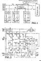
- FIG. 1 a StarLAN (an acronym for Star Local Area Network) daisy chain arrangement in which a plurality of transceivers DTE #1, DTE #2, ...DTE #n are star-connected (i.e., a star topology network) to a shared hub 10 via two twisted pairs of transmission lines 12 and 14.
- Each of the transceivers DTE #1, ...DTE #n consists of respective transmitters TxD1, ...TxDn and respective receivers RxD1, ...RxDn.
- the twisted pair of transmission lines 12 defining a transmit channel is connected to each of the transmitters DTE #1, ...DTE #n via isolation transformers 16.
- the twisted pair of transmission lines 14 defining a receive channel is connected to each of the receivers Rx01, ...RxOn via isolation transformers 18.
- the hub 10 repeats the transmitted signals and sends them to all of the other transceivers.
- two or more transmitters are transmitting concurrently referred to as a "collision" it is needed to detect a StarLAN daisy chain collision condition at each active transmitter.
- a collision detector circuit connected between each of the transmitters and the isolation transformers 16 at the place marked by an "X".
- This prior art collision detection circuit was formed of a peak detector circuit utilizing a fixed D.C. reference voltage of approximately +5.U volts ⁇ 5%. Since the output voltage of the transmitter is susceptible to variations due to changes in the load, the peak detector circuit could be falsely triggered at times to indicate a collision when there was none thereby limiting the reliability and accuracy thereof. Also, sensitivity to collisions was limited due to the need to maintain adequate margins between the reference voltage and the peak voltage under all operating conditions of the transmitters. Thus, there is a need for improvements in such daisy chain collision detection circuits to provide a more accurate referenced voltage which is proportional to the peak output voltage of the transmitter.
- the present invention is concerned with the provision of a daisy chain collision detection circuit for use with a StarLAN coded data transceiver which includes a voltage comparator, first and second input nodes, first and second rectifiers, a first voltage divider, a second voltage divider, and a first charging capacitor.
- the voltage comparator has an inverting input, a non-inverting input, and an output.
- the first and second input nodes receive differential output voltages from a differential line driver and transient spike voltages from the primary of an-isolation transformer.
- the first rectifier is connected between the first input node and a first -intermediate node.
- the second rectifier is connected between the second input node and the first intermediate node.
- the first voltage divider is formed of a series connection-of a first resistor and a second resistor.
- the first voltage divider is coupled between the input nodes and a second intermediate node.
- the junction of the first resistor and the second resistor is connected to the inverting input of the voltage comparator.
- the second voltage divider is formed of a series connection of a third resistor and a fourth resistor.
- the second voltage divider is connected between the first intermediate node and the second intermediate node.
- the junction of the third resistor and the fourth resistor is connected to the non-inverting input of the voltage comparator.
- the first charging capacitor is connected between the non-inverting input of the voltage comparator and the second intermediate node. The first charging capacitor is charged to a voltage which is directly proportional to the peak voltage of the differential output voltages.
- FIG. 2 of the drawings there is illustrated a detailed schematic circuit diagram of a .daisy chain collision detection circuit 20 for use with a StarLAN coded data transceiver.
- the detection circuit 20 of the present invention is connected between the output of a transmitter U1 in the transceiver and the primary winding P of an isolation transformer. T1.
- the transmitter U1 and the isolation transformer T1 correspond to the transmitters TxD1, ...TxDn and the respective transformers 16 shown in Figure 1.
- the transmitter U1 consists of a differential line driver which is similar to one that is commercially available from Advanced Micro Devices, Inc. of Sunnyvale, California and designated with their Part No. Am26LS30.
- the line driver U1 receives a single-ended digital data input signal TxD via line 24 and converts the same to differential output signals appearing at nodes A and B:
- a capacitor C1 is connected across the nodes A and B defining the differential outputs of the line driver U1.
- the capacitor C1 acts as a low-pass filter to eliminate high-frequency noise and as a slew rate limiter.
- the digital data input signal TxD is a Manchester encoded data transmission signal generated by a LAN (local area network) controller (not shown) of the type manufactured by Intel Corporation under the designation B2586.
- the StarLAN differential output signals are voltages having peak amplitude variations between +2.0 volts and +3.65 volts.
- the line driver U1 also receives an enable signal EN via line 26 for activating the same.
- an enable signal EN via line 26 for activating the same.
- the line driver U1 is disabled and is set to the tri-state mode.
- the line driver U1 becomes activated.
- the collision detection circuit 20 includes a. high-speed voltage comparator U2 which is similar to one that is commercially available from National Semiconductor Corporation of Santa Clara, California under their part No. LM319.
- the ends of the filter capacitor C1 connected across the nodes A and B also form inputs of the collision detection circuit.
- the end of the capacitor C1 connected to the input node A is also connected to the anode of a diode CR1, and the other end of the capacitor C1 connected to the input node 8 is also connected to the anode of a diode CR2.
- the cathode of the diode CR1 is tied to the cathode of the diode CR2 at an intermediate node C.
- the input node A is coupled to one end of a first voltage divider formed of series-connected resistors R1 and R2.
- the other end of resistor R2 is connected to an intermediate node D.
- the junction of the 'resistors R1 and R2 defines a node E which is connected to the inverting input of the voltage comparator U2.
- the intermediate node C is connected to one end of a second voltage divider formed of series-connected resistors R3 and R4.
- the other end of the resistor R4 is connected to the intermediate node D.
- the junction of the resistors R3 and R4 defines a node F which is connected to the non-inverting input of the voltage comparator U2.
- a first charging capacitor C2 has its one end connected to the node F and the non-inverting input of the voltage comparator U2. The other end of the capacitor C2 is connected to the intermediate node D.
- a second charging capacitor C3 is connected in parallel with the resistor R2 which is interconnected between the node E and the intermediate node D.
- the capacitor C3 serves as a single pole filter with a small time constant which integrates any fast rising slew voltage spikes that may be present at the input nodes A and B.
- the first charging capacitor C2 also serves as a single pole filter with a larger time constant than the network formed by the first voltage divider (R1, R2) and the second charging capacitor C3.
- the capacitor C3 causes a small time delay of any voltage spikes appearing at the node E relative to the node P so as to prevent false triggering of the voltage comparator U2 when the line driver U1 is transmitting a message.
- the voltage comparator U2 is connected to a dual polarity power source having a positive.voltage V1 and a negative voltage V2.
- a filter capacitor C4 is connected between the positive voltage V1 and a ground potential for eliminating any high frequency noise.
- a filter capacitor C5 is connected between the negative voltage V2 and the ground potential for eliminating any high frequency noise. It should be understood that a comparator requiring only a single polarity power source could be used instead of the voltage comparator U2 which utilizes the dual polarity power source.
- the voltage comparator U2 has an open collector output which requires an external resistor load.
- a third voltage divider formed of series-connected resistors R5 and R6 is provided to serve as the external load.
- the junction of the resistors R5 and R6 defines a node G which is connected to the output of the voltage comparator U2.
- the other end of the resistor R5 is connected to a supply voltage or potential VCC which is typically at +5.0 volts.
- the other end of the resistor R6 is connected to the ground potential.
- third and fourth diodes CR3 and CR4 which are coupling means, so that the two voltages appearing at the nodes E and F will move with similar temperature coefficients.
- the third and fourth diodes serve to balance the potential drop and non-linearity with temperature across the first and second diodes.
- the anode of the diode CR3 is connected to the input node A and the anode of the diode CR4 is connected to the input node B.
- the cathode of the diode CR3 is tied to the cathode of the diode CR4 at an' intermediate node H.
- the node H is connected to the resistor R1 of the first voltage divider.
- a collision output latch is formed of a first two-input NAND gate U3 and a second three-input NANO gate U4.
- the output of the first NAND gate U3 is connected to the input of the second NAND gate U4 via line 11, and the output of the second NAND gate U4 is connected to the input of the first NAND gate U3 via line 13.
- the other input of the first NAND gate U3 defines a set input on line 15 which is connected to the output of the voltage comparator U2 at the node G.
- the other inputs of the second NAND gate U4 define a first reset input on line 17 and a second reset input on line 19.
- the output of the latch is at the output of the second NAND gate U4 which is connected to line 30 to provide an external collision presence signal ECDT.
- the collision output latch functions to insure the capture and retention of narrow spikes (signals having a short duration) from the output of the comparator U3.
- a time delay circuit includes a first D-type flip-flop U5 and a second 0-type flip-flop U6 which are connected together as a shift register.
- the first flip-flop U5 has its data input connected to the enable signal EN via the line 26 and its clock input connected to a 1 MHz clock signal via line 28.
- the Q output of the first flip-flop U5 is connected to the data input of the second flip-flop U6 via line 21.
- the second flip-flop U6 has its clock input also connected to the 1 MHz clock signal at the line 28 and its Q output connected to the first reset input of the collision output latch via the line 17.
- the time delay circuit creates a delay immediately after the line driver U1 is enabled (when the enable signal is switched from the high logic level to the low logic level) which prevents false triggering of the voltage comparator U2 during the time when the capacitors C2 and C3 are being fully charged.
- a disabling means is provided for reducing the load imposed on the network through the primary winding of the isolation transformer when the line driver U1 is inactive by the first and second voltage dividers which is reflected into the secondary of the isolation transformer.
- the total load imposed by the network of inactive transmitters connected to the twisted pair of transmission lines 12 is thereby reduced.
- the disabling means is formed of an NPN-type transistor Q1, a current-limiting resistor R7 and an inverter U8, One end of the resistor R7 is connected to the supply potential VCC, and the other end of the resistor R7 is connected to the base of the transistor Q1.
- the base of the transistor Q1 is also connected to the output of the inverter U8.
- the input of the inverter U8 is connected .to receive the enable signal EN on the line 26.
- the transistor Q1 has its collector connected to the intermediate node D and its emitter connected to a ground potential.
- the node A is further connected to one end of the primary side P of the isolation transformer T1
- the input node B is further connected to the other end of the primary side P of the isolation transformer T1.
- the secondary side 5 of the isolation transformer T1 is connected to the twisted pair of the transmission lines 12 ( Figure 1).
- An inverter U7 has its input connected to receive also the enable signal EN on the line 26 and its output connected to the second reset input of the collision output ' latch via the line 19.
- the transistor Q1 of the disabling means is rendered conductive so as to be in the low resistance state, thereby linking the intermediate node D to the ground potential.
- the voltages V E and V F at the corresponding nodes E and F connected to the respective inverting and non-inverting inputs of the voltage comparator U2 will be produced as determined by the resistance values in the corresponding first and second voltage dividers.
- the transistor Q1 When the line driver U1 is disabled or not transmitting, the transistor Q1 is rendered non-conductive so as to be in the high resistance state which causes the output of the comparator to be in an indeterminate state. Therefore, in order to prevent 'false triggering of the voltage comparator U2 immediately after the line driver U1 is disabled (when the enable signal is switched from the low logic level to the high logic level), the output of the inverter U7 will be switched to the low logic state at the end of transmission. As a consequence, the output of the latch on the line 30 will be reset to a high logic level, thereby indicating that no collision has occurred.
- the differential output signals from the differential line driver U1 are received at the input nodes A and B when the enable signal EN on the line 26 is at the low or "0" logic level.
- the enable signal EN is in the high or "1" logic level
- the line driver is disabled. Assuming that the line driver U1 has been activated, the single-ended digital data input signal TxD on the line 24 will cause the differential output signals to appear at the nodes A and B of the collision detection circuit 20. Since the transistor Q1 will be rendered conductive, the first charging capacitor C2 and the second charging capacitor C3 will be charged up to the node voltages V F and V E at the respective nodes F and E.
- the voltage V F on the first charging capacitor C2 at the node F produces a reference voltage and is directly proportional to the peak voltage of the differential output voltages from the line driver U1 across the input nodes A and B. While the absolute DC voltages at the nodes E and F will change as a function of the differential output voltages from the line driver and the loading imposed by other transmitters, the differential voltage between the nodes E and F will be substantially constant.
- the difference between the voltages V F and V E represents the operating margin when only the line driver U1 is active and there are no collisions occurring (no other transmitter in the DTE's is transmitting).
- the node voltage V F at the non-inverting input will be at a higher potential than the node voltage V E at the inverting input of the voltage comparator U2. Consequently, the comparator U2 compares these two voltages and causes its output at the node G on the line 15 to be driven to its higher voltage state which has an upper voltage level defined by the load resistors R5 and R6 of the third voltage divider. This higher voltage from the comparator will maintain the output of the NAND gate U3 of the latch at a low logic level. Thus, the output of the NAND gate U4 or the external collision presence signal ECDT on the line 30 will be at a high logic level indicating that no daisy chain collision has taken place.
- the node voltage V E will become transiently more positive than the node voltage V F so as to generate narrow negative pulses at the output of the comparator at the node G.
- the output of the voltage comparator provides an internal collision detection signal which is switched from a high logic level to a low logic level upon the occurrence of a daisy chain collision. This low logic level will cause the output of the NAND gate U3 to change to the high logic level.
- the output of the NAND gate U4 or the external collision presence signal will be switched from the high logic level to the low logic level indicating that a collision has occurred. This low logic level will be maintained until the end of transmission when the enable signal EN is switched back to the high logic level.
- the output of the inverter U7 will be switched immediately to the low logic level so as to reset the output of the NAND gate U4 to the high logic level.
- the Q output of the flip-flop U6 in the time delay circuit will also be at the low logic level after a short time delay which also resets the output of the NAND gate U4.
- the Q output of the flip-flop U6 will be maintained in the low logic level immediately after the line driver U1 is enabled so as to allow the capacitors C2 and C3 to reach their full charge. Accordingly, any false collision indications by the voltage comparator will not be latched and the external collision presence signal ECDT will remain at the high logic level during this time.
- the output of the voltage comparator will be allowed to change to the low logic level and thus switch the external collision presence signal to the low logic upon the occurrence of an actual collision.
- the present invention provides an improved daisy chain collision detection circuit having a more accurate referenced voltage which is proportional to the peak output voltage of the transmitter. Further, there is provided a disabling means for reducing the load to the line driver imposed by the network of inactive transmitters daisy chained together.
Priority Applications (1)
| Application Number | Priority Date | Filing Date | Title |
|---|---|---|---|
| AT87307250T ATE94011T1 (de) | 1986-12-12 | 1987-08-17 | Kollisionserkennungsschaltung fuer daisy chain. |
Applications Claiming Priority (2)
| Application Number | Priority Date | Filing Date | Title |
|---|---|---|---|
| US941238 | 1986-12-12 | ||
| US06/941,238 US4710943A (en) | 1986-12-12 | 1986-12-12 | Starlan coded data transceiver collision detection circuit |
Publications (3)
| Publication Number | Publication Date |
|---|---|
| EP0271179A2 true EP0271179A2 (de) | 1988-06-15 |
| EP0271179A3 EP0271179A3 (en) | 1990-04-04 |
| EP0271179B1 EP0271179B1 (de) | 1993-09-01 |
Family
ID=25476153
Family Applications (1)
| Application Number | Title | Priority Date | Filing Date |
|---|---|---|---|
| EP87307250A Expired - Lifetime EP0271179B1 (de) | 1986-12-12 | 1987-08-17 | Kollisionserkennungsschaltung für daisy chain |
Country Status (6)
| Country | Link |
|---|---|
| US (1) | US4710943A (de) |
| EP (1) | EP0271179B1 (de) |
| JP (1) | JP2547586B2 (de) |
| AT (1) | ATE94011T1 (de) |
| DE (1) | DE3787260T2 (de) |
| ES (1) | ES2044940T3 (de) |
Families Citing this family (5)
| Publication number | Priority date | Publication date | Assignee | Title |
|---|---|---|---|---|
| JP2548693B2 (ja) * | 1985-03-13 | 1996-10-30 | キヤノン株式会社 | シリアルデータ通信方式および装置 |
| DE3776782D1 (de) * | 1986-12-12 | 1992-03-26 | Siemens Nixdorf Inf Syst | Sende-empfangs-einrichtung fuer ein busleitungssystem. |
| US5043722A (en) * | 1989-01-30 | 1991-08-27 | Honeywell Inc. | Detector for colliding signals in asynchronous communication |
| US5425054A (en) * | 1993-06-23 | 1995-06-13 | Tamarack Microelectronics Inc. | Surrounding circuit for the ethernet coaxial local area newtwork transceiver |
| US5430396A (en) * | 1994-07-27 | 1995-07-04 | At&T Corp. | Backplane bus for differential signals |
Citations (4)
| Publication number | Priority date | Publication date | Assignee | Title |
|---|---|---|---|---|
| US4479228A (en) * | 1981-03-11 | 1984-10-23 | 3Com Corporation | Local computer network transceiver |
| JPS6028340A (ja) * | 1983-07-26 | 1985-02-13 | Nec Corp | 信号衝突検出回路 |
| US4516248A (en) * | 1983-01-21 | 1985-05-07 | E-Systems, Inc. | Variable threshold receiver |
| EP0195595A2 (de) * | 1985-03-21 | 1986-09-24 | AT&T Corp. | Lokales Netzwerk |
Family Cites Families (3)
| Publication number | Priority date | Publication date | Assignee | Title |
|---|---|---|---|---|
| US4649548A (en) * | 1981-03-11 | 1987-03-10 | Crane Ronald C | Local computer network transceiver |
| US4476467A (en) * | 1982-06-08 | 1984-10-09 | Cromemco Inc. | Random entry intercomputer network with collision prevention |
| US4519074A (en) * | 1983-05-31 | 1985-05-21 | Rca Corporation | Transceiver having collision detection capability for contention-formatted FDM local area networks |
-
1986
- 1986-12-12 US US06/941,238 patent/US4710943A/en not_active Expired - Lifetime
-
1987
- 1987-08-17 ES ES87307250T patent/ES2044940T3/es not_active Expired - Lifetime
- 1987-08-17 DE DE87307250T patent/DE3787260T2/de not_active Expired - Fee Related
- 1987-08-17 AT AT87307250T patent/ATE94011T1/de not_active IP Right Cessation
- 1987-08-17 EP EP87307250A patent/EP0271179B1/de not_active Expired - Lifetime
- 1987-09-02 JP JP62220094A patent/JP2547586B2/ja not_active Expired - Fee Related
Patent Citations (4)
| Publication number | Priority date | Publication date | Assignee | Title |
|---|---|---|---|---|
| US4479228A (en) * | 1981-03-11 | 1984-10-23 | 3Com Corporation | Local computer network transceiver |
| US4516248A (en) * | 1983-01-21 | 1985-05-07 | E-Systems, Inc. | Variable threshold receiver |
| JPS6028340A (ja) * | 1983-07-26 | 1985-02-13 | Nec Corp | 信号衝突検出回路 |
| EP0195595A2 (de) * | 1985-03-21 | 1986-09-24 | AT&T Corp. | Lokales Netzwerk |
Non-Patent Citations (2)
| Title |
|---|
| ELECTRONIC ENGINEERING, vol. 57, no. 698, February 1985, page 13, London, GB; "Intel's new chip key to PC networks" * |
| PATENT ABSTRACTS OF JAPAN, vol. 9, no. 147 (E-323)[1870], 21st June 1985; & JP-A-60 28 340 (NIPPON DENKI K.K.) 13-02-1985 * |
Also Published As
| Publication number | Publication date |
|---|---|
| DE3787260D1 (de) | 1993-10-07 |
| DE3787260T2 (de) | 1994-02-24 |
| ES2044940T3 (es) | 1994-01-16 |
| JPS63157542A (ja) | 1988-06-30 |
| EP0271179A3 (en) | 1990-04-04 |
| US4710943A (en) | 1987-12-01 |
| ATE94011T1 (de) | 1993-09-15 |
| JP2547586B2 (ja) | 1996-10-23 |
| EP0271179B1 (de) | 1993-09-01 |
Similar Documents
| Publication | Publication Date | Title |
|---|---|---|
| EP0843416B1 (de) | Sperrungs- und Statusanzeigeschaltung | |
| US4479228A (en) | Local computer network transceiver | |
| US20040207431A1 (en) | Logic isolator | |
| US4649548A (en) | Local computer network transceiver | |
| US4384363A (en) | Transceiver for local network using carrier-sense multiple access/collision detection | |
| US5355390A (en) | Communication apparatus for transmitting and receiving communication signals through common transmission line | |
| US4380088A (en) | Tester for collision-detect circuitry | |
| US4412347A (en) | Precision setting of currents and reference voltages | |
| EP0271179B1 (de) | Kollisionserkennungsschaltung für daisy chain | |
| US5263049A (en) | Method and apparatus for CMOS differential drive having a rapid turn off | |
| US5198700A (en) | Doubletpulse generator | |
| EP0116603A4 (de) | Gerät zum senden und empfangen digitaler signale. | |
| US6538865B1 (en) | Fault-detecting device for communication system | |
| JP2988529B2 (ja) | 故障診断装置 | |
| JP4611421B2 (ja) | 論理しきい値取得回路および逆ピーク検出器を使用する方法 | |
| US4734596A (en) | Detection of direct current in the presence of manchester-encoded signals | |
| US3369075A (en) | Transmission system for direct current level binary data | |
| RU2543963C2 (ru) | Приемник в шинном узле шинной сети | |
| JPH03254246A (ja) | Lan用伝送システム | |
| KR910002355B1 (ko) | 주장치와 키폰전화기간의 직렬 데이타 송수신 전달회로 | |
| JPH01147943A (ja) | データ受信回路 | |
| JPH01317007A (ja) | バスインタフェース受信回路 | |
| JPH01221044A (ja) | 信号伝送装置 | |
| JPS61238143A (ja) | バス形ネツトワ−ク送信装置 | |
| JPH0490641A (ja) | 衝突検出装置 |
Legal Events
| Date | Code | Title | Description |
|---|---|---|---|
| PUAI | Public reference made under article 153(3) epc to a published international application that has entered the european phase |
Free format text: ORIGINAL CODE: 0009012 |
|
| AK | Designated contracting states |
Kind code of ref document: A2 Designated state(s): AT BE CH DE ES FR GB GR IT LI LU NL SE |
|
| PUAL | Search report despatched |
Free format text: ORIGINAL CODE: 0009013 |
|
| AK | Designated contracting states |
Kind code of ref document: A3 Designated state(s): AT BE CH DE ES FR GB GR IT LI LU NL SE |
|
| 17P | Request for examination filed |
Effective date: 19900306 |
|
| 17Q | First examination report despatched |
Effective date: 19920410 |
|
| GRAA | (expected) grant |
Free format text: ORIGINAL CODE: 0009210 |
|
| AK | Designated contracting states |
Kind code of ref document: B1 Designated state(s): AT BE CH DE ES FR GB GR IT LI LU NL SE |
|
| REF | Corresponds to: |
Ref document number: 94011 Country of ref document: AT Date of ref document: 19930915 Kind code of ref document: T |
|
| REF | Corresponds to: |
Ref document number: 3787260 Country of ref document: DE Date of ref document: 19931007 |
|
| ITF | It: translation for a ep patent filed |
Owner name: ING. C. GREGORJ S.P.A. |
|
| ET | Fr: translation filed | ||
| REG | Reference to a national code |
Ref country code: ES Ref legal event code: FG2A Ref document number: 2044940 Country of ref document: ES Kind code of ref document: T3 |
|
| REG | Reference to a national code |
Ref country code: GR Ref legal event code: FG4A Free format text: 3009876 |
|
| PLBE | No opposition filed within time limit |
Free format text: ORIGINAL CODE: 0009261 |
|
| STAA | Information on the status of an ep patent application or granted ep patent |
Free format text: STATUS: NO OPPOSITION FILED WITHIN TIME LIMIT |
|
| 26N | No opposition filed | ||
| EAL | Se: european patent in force in sweden |
Ref document number: 87307250.8 |
|
| PGFP | Annual fee paid to national office [announced via postgrant information from national office to epo] |
Ref country code: SE Payment date: 19970717 Year of fee payment: 11 |
|
| PGFP | Annual fee paid to national office [announced via postgrant information from national office to epo] |
Ref country code: AT Payment date: 19970723 Year of fee payment: 11 |
|
| PGFP | Annual fee paid to national office [announced via postgrant information from national office to epo] |
Ref country code: GR Payment date: 19970725 Year of fee payment: 11 |
|
| PGFP | Annual fee paid to national office [announced via postgrant information from national office to epo] |
Ref country code: BE Payment date: 19970908 Year of fee payment: 11 |
|
| PGFP | Annual fee paid to national office [announced via postgrant information from national office to epo] |
Ref country code: LU Payment date: 19970911 Year of fee payment: 11 |
|
| PGFP | Annual fee paid to national office [announced via postgrant information from national office to epo] |
Ref country code: CH Payment date: 19971014 Year of fee payment: 11 |
|
| PG25 | Lapsed in a contracting state [announced via postgrant information from national office to epo] |
Ref country code: LU Free format text: LAPSE BECAUSE OF NON-PAYMENT OF DUE FEES Effective date: 19980817 Ref country code: AT Free format text: LAPSE BECAUSE OF NON-PAYMENT OF DUE FEES Effective date: 19980817 |
|
| PG25 | Lapsed in a contracting state [announced via postgrant information from national office to epo] |
Ref country code: SE Free format text: LAPSE BECAUSE OF NON-PAYMENT OF DUE FEES Effective date: 19980818 |
|
| PG25 | Lapsed in a contracting state [announced via postgrant information from national office to epo] |
Ref country code: LI Free format text: LAPSE BECAUSE OF NON-PAYMENT OF DUE FEES Effective date: 19980831 Ref country code: GR Free format text: LAPSE BECAUSE OF NON-PAYMENT OF DUE FEES Effective date: 19980831 Ref country code: CH Free format text: LAPSE BECAUSE OF NON-PAYMENT OF DUE FEES Effective date: 19980831 Ref country code: BE Free format text: LAPSE BECAUSE OF NON-PAYMENT OF DUE FEES Effective date: 19980831 |
|
| BERE | Be: lapsed |
Owner name: ADVANCED MICRO DEVICES INC. Effective date: 19980831 |
|
| REG | Reference to a national code |
Ref country code: CH Ref legal event code: PL |
|
| EUG | Se: european patent has lapsed |
Ref document number: 87307250.8 |
|
| REG | Reference to a national code |
Ref country code: GB Ref legal event code: IF02 |
|
| PGFP | Annual fee paid to national office [announced via postgrant information from national office to epo] |
Ref country code: NL Payment date: 20020618 Year of fee payment: 16 |
|
| PGFP | Annual fee paid to national office [announced via postgrant information from national office to epo] |
Ref country code: GB Payment date: 20020626 Year of fee payment: 16 |
|
| PGFP | Annual fee paid to national office [announced via postgrant information from national office to epo] |
Ref country code: FR Payment date: 20020805 Year of fee payment: 16 |
|
| PGFP | Annual fee paid to national office [announced via postgrant information from national office to epo] |
Ref country code: ES Payment date: 20020827 Year of fee payment: 16 |
|
| PGFP | Annual fee paid to national office [announced via postgrant information from national office to epo] |
Ref country code: DE Payment date: 20020830 Year of fee payment: 16 |
|
| PG25 | Lapsed in a contracting state [announced via postgrant information from national office to epo] |
Ref country code: GB Free format text: LAPSE BECAUSE OF NON-PAYMENT OF DUE FEES Effective date: 20030817 |
|
| PG25 | Lapsed in a contracting state [announced via postgrant information from national office to epo] |
Ref country code: ES Free format text: LAPSE BECAUSE OF NON-PAYMENT OF DUE FEES Effective date: 20030818 |
|
| PG25 | Lapsed in a contracting state [announced via postgrant information from national office to epo] |
Ref country code: NL Free format text: LAPSE BECAUSE OF NON-PAYMENT OF DUE FEES Effective date: 20040301 |
|
| PG25 | Lapsed in a contracting state [announced via postgrant information from national office to epo] |
Ref country code: DE Free format text: LAPSE BECAUSE OF NON-PAYMENT OF DUE FEES Effective date: 20040302 |
|
| GBPC | Gb: european patent ceased through non-payment of renewal fee |
Effective date: 20030817 |
|
| PG25 | Lapsed in a contracting state [announced via postgrant information from national office to epo] |
Ref country code: FR Free format text: LAPSE BECAUSE OF NON-PAYMENT OF DUE FEES Effective date: 20040430 |
|
| NLV4 | Nl: lapsed or anulled due to non-payment of the annual fee |
Effective date: 20040301 |
|
| REG | Reference to a national code |
Ref country code: FR Ref legal event code: ST |
|
| REG | Reference to a national code |
Ref country code: ES Ref legal event code: FD2A Effective date: 20030818 |
|
| PG25 | Lapsed in a contracting state [announced via postgrant information from national office to epo] |
Ref country code: IT Free format text: LAPSE BECAUSE OF NON-PAYMENT OF DUE FEES;WARNING: LAPSES OF ITALIAN PATENTS WITH EFFECTIVE DATE BEFORE 2007 MAY HAVE OCCURRED AT ANY TIME BEFORE 2007. THE CORRECT EFFECTIVE DATE MAY BE DIFFERENT FROM THE ONE RECORDED. Effective date: 20050817 |