EP0268532A2 - Signalverarbeitungseinrichtung - Google Patents
Signalverarbeitungseinrichtung Download PDFInfo
- Publication number
- EP0268532A2 EP0268532A2 EP87402560A EP87402560A EP0268532A2 EP 0268532 A2 EP0268532 A2 EP 0268532A2 EP 87402560 A EP87402560 A EP 87402560A EP 87402560 A EP87402560 A EP 87402560A EP 0268532 A2 EP0268532 A2 EP 0268532A2
- Authority
- EP
- European Patent Office
- Prior art keywords
- signal
- level
- input signal
- circuits
- amplitude
- Prior art date
- Legal status (The legal status is an assumption and is not a legal conclusion. Google has not performed a legal analysis and makes no representation as to the accuracy of the status listed.)
- Granted
Links
Images


Classifications
-
- H—ELECTRICITY
- H03—ELECTRONIC CIRCUITRY
- H03H—IMPEDANCE NETWORKS, e.g. RESONANT CIRCUITS; RESONATORS
- H03H11/00—Networks using active elements
- H03H11/02—Multiple-port networks
- H03H11/26—Time-delay networks
-
- H—ELECTRICITY
- H03—ELECTRONIC CIRCUITRY
- H03H—IMPEDANCE NETWORKS, e.g. RESONANT CIRCUITS; RESONATORS
- H03H17/00—Networks using digital techniques
- H03H17/0009—Time-delay networks
-
- H—ELECTRICITY
- H03—ELECTRONIC CIRCUITRY
- H03H—IMPEDANCE NETWORKS, e.g. RESONANT CIRCUITS; RESONATORS
- H03H19/00—Networks using time-varying elements, e.g. N-path filters
Definitions
- the present invention generally relates to signal processing circuits, and in particular to a signal processing circuit for delaying an input signal by a predetermined time.
- the present invention is applicable to filter circuits for an analog signal or a digital signal.
- delay circuits are widely used as a signal processing circuit for delaying an input signal by a predetermined time.
- the delay circuits are generally classified into two types, one of which is an analog delay circuit and the other is a digital delay circuit.
- ultrasonic delay lines such as a comb line filter are known as an analog delay circuit
- shift registers are known as a digital delay circuit.
- the delay circuits are used for filters for filtering an input signal to produce an output signal having desirable frequency components.
- the conventional delay circuits using the ultrasonic delay lines have a disadvantage that the size is physically limited and therefore delay circuits of compact size are not obtainable.
- the frequency components to be eliminated are not changed even when the frequency of the input signal varies.
- a general object of the present invention is to provide a novel and useful signal processing circuit in which the disadvantages mentioned above have been eliminated.
- a more specific object of the present invention is to provide a signal processing circuit having a circuit simpler than circuits of conventional delay circuits.
- Another object of the present invention is to provide a signal processing circuit capable of producing a signal having a delay amount which follows up a frequency of an input signal.
- Still another object of the present invention is to provide a signal processing circuit having a filtering function obtainable by use of a delayed input signal.
- a further object of the present invention is to provide a signal processing corcuit which may be suitably implemented by a semiconductor integrated circuit.
- a signal processing circuit comprising a constant value generating circuit for generating a constant value ( ⁇ i ) corresponding to a delay time (d i ) for an input signal (V i (t)); an adding/subtracting circuit for alternately adding the constant value to the input signal and subtracting the constant value from the input signal for every half period of the input signal; and an amplitude correcting circuit for correcting an amplitude of an output signal of the adding/subtracting circuit for every half period of the input signal so that an output signal (V o (t)) having a waveform corresponding to a waveform of the input signal is produced.
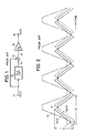
- FIG.1 is a block diagram of a conventional signal processing circuit including a delay circuit, for eliminating frequency components from an input signal
- FIGS.2 and 3 are views showing waveforms at parts in the configuration shown in FIG.1.
- FIG.1 is designed so as to process digital signals, an explanation below will be given with respect to analog signal waveforms corresponding to the digital signals to facilitate a better understanding.
- the input signal V1(t) is a triangular wave signal.
- the input signal V1(t) is delayed by a delay amount d1 with respect to the original input signal V1(t) by the delay circuit 12, which is composed of shift registers.
- An output signal x1 of the delay circuit 12 is fed to one input of an adder 13, the other input of which receives the input signal V1(t) through the terminal 11.
- An added result x2 derived from the adder 13 is supplied to a 1/2 level attenuator 14, which attenuates a level of the signal x2 by 1/2.
- An output signal V o1 (t) from the attenuator 14 appears at an output terminal 15. As shown in FIG.2, the output signal V o1 (t) has flat signal parts. This means that some frequency components have been eliminated from the input signal V1(t).
- FIG.3 shows waveforms in a case where an input signal V2(t) which has a peak value V2 (identical to the peak value v1) and a period T2 longer than the period T1, is applied to the input terminal 11.
- the input signal V2(t) is delayed by a delay amount d2, and is attenuated by 1/2 level, so that an output signal V o2 (t) is produced.
- V i (t) an input signal such as the signal V1(t) or V2(t)
- V o1 (t) or V o2 (t) an output signal such as V o1 (t) or V o2 (t)
- d i a delay amount such as the delay amount d1 or d2
- V i (t-d i ) in the equation (1) is expressed as the following equation (2): V i (t-d i ) ⁇ V i (t) ⁇ ⁇ i (2).
- ⁇ i 2v i ⁇ d i / T i
- v i is a peak value of the input signal V i (t) and T i is a period of the input signal V i (t).
- the conventional signal processing circuit described in the foregoing has a disadvantage that the circuit scale of the delay circuit 12 is large, because the circuit 12 is formed by the multi-stage cascade connection of the shift registers formed by flip-flops, for example.
- FIG.4 shows an amplitude of the input signal V i (t) versus a delay time for explaining a relationship between a number of shift registers and a delay amount.
- a three-stage cascade connection of flip-flops each having a unit delay time ⁇ is necessary to produce an output signal V o3 having a delay amount (t3 - t0) with respect to the input signal V i (t).
- a five-stage cascade connection of flip-flops is necessary to produce an output signal V o5 having a delay amount (t5 - t0) with respect to the input signal V i (t).
- the conventional signal processing circuit described above has the following disadvantage.
- a situation is considered in which the input signal V i (t) is delayed by a delay time which corresponds to a frequency of the input signal.
- the input signal V1 having a frequency of 1/T1 is delayed by the delay time d1 as shown in FIG.2
- the input signal V2(t) is delayed by the delay time d2 having a frequency of 1/T2, as shown in FIG.3.
- it is intended to vary the delay time with respect to the input signal V i (t) in response to a variation in the frequency thereof in the conventional circuit structure it is necessary to adjust a frequency of a clock signal supplied to the delay circuit 12 or to vary the number of stages of the cascade configuration. These adjustments are cumbersome.
- the present invention mainly intends to eliminate these problems.
- an input signal V i (t) is passed through an input terminal 21 and applied to an adding/subtracting circuit 22.
- a constant value generating circuit 23 generates a constant value ⁇ i corresponding to a delay amount d i with respect to the input signal V i (t).
- the constant value ⁇ i is supplied to the adding/subtracting circuit 22.
- the adding/subtracting circuit 22 alternately carries out a subtracting operation of the constant value ⁇ i from the input signal V i (t) and an adding operation of the constant value ⁇ i to the input signal V i (t), for every period which is half of the period T i of the input signal V i (t).
- An output signal of the adding/subtracting circuit 22 is fed to an amplitude correcting circuit 24.
- the circuit 24 performs the amplitude correction for the output signal of the addition/subtraction circuit 24 for every 1/2 period of the input signal V i (t).
- An output signal V o (t) of the amplitude correcting circuit 24 is supplied to an external circuit through an output terminal 25.
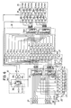
- FIG.6 is a circuit diagram of the block configuration shown in FIG.5.
- FIGS.7(A) through 7(G) show waveforms of signals at different parts of the circuit configuration shown in FIG.6.
- An illustrated circuit structure is designed so as to process the digital input signal V i (t) composed of 8 bits.
- V i (t) composed of 8 bits.
- the input signal V i (t) composed of 8 bits Q0, Q2,..., and Q7 is applied to the adding/subtracting circuit 22 through the input terminal 21.
- the input signal V i (t) has a triangular wave signal as shown in FIG.7(A).
- the adding/subtracting circuit 22 also receives the constant value ⁇ i composed of 8 bits which are produced by the constant value generating circuit 23.
- the constant value generating circuit 23 consists of 8 exclusive-OR circuits 230, 231,..., 237. A high-level signal (H) or a low-level signal (L) is applied to each exclusive-OR circuit in accordance with the constant value ⁇ i to be produced.
- the constant value generating circuit 23 produces the constant value ⁇ i in response to a timing signal SC().
- the signal SC() is a signal obtained by inverting a carry signal SC(Q) supplied from a terminal 26 by an inverter 31.
- the carry signal SC(Q) has a period half of the period T i of the input signal V i (t), as shown in FIG.7(C).
- the adding/subtracting circuit 22 which alternately performs the adding operation and the subtracting operation, includes two 4-bit binary full adders 221 and 222.
- the adders 221 and 222 each have input terminals A1, A2, A3 and A4 and B1, B2, B3 and B4.
- the terminals A1, A2, A3 and A4 of the adder 221 receive the input signals Q0, Q1, Q2 and Q3, respectively.
- the terminals A1, A2, A3 and A4 of the adder 222 receive the input signals Q4, Q5, Q6 and Q7, respectively.
- the terminals B1, B2, B3 and B4 of the adder 221 receive the outputs of the exclusive-OR circuits 230, 231, 232 and 233, respectively.
- the terminals B1, B2, B3 and B4 of the adder 222 receive the outputs of the exclusive-OR circuits 234, 235, 236 and 237, respectively.
- the signal SC() from the inverter 31 is applied to a carry input terminal C0 of the adder 221.
- the adders 221 and 222 carry out the adding operation or the subtracting operation in accordance with timings defined by the signal SC(Q). In detail, when the signal SC(Q) is kept low, the adders 221 and 222 carry out the subtracting operation, whereas when the signal SC(Q) is kept high, the adders 221 and 222 carry out the adding operation.
- An added or subtracted result S0 between A1 and B1 of the adder 221 appears at a terminal E1 thereof.
- calculated results S1, S2 and S3 between A2 and B2; A3 and B3; and A4 and B4 of the adder 221 appear at terminals E2, E3 and E4 thereof, respectively.
- calculated results S4, S5, S6 and S7 are obtained at terminals E1, E2, E3 and E4 of the adder 222, respectively.
- a carry output C4 of the adder 221 is fed to a carry input C0 of the adder 222.
- FIG.7(B) An analog output signal corresponding to the binary signals S0 - S7 is shown by a solid line in FIG.7(B).
- the adding/subtracting circuit 22 subtracts the constant value ⁇ i from the input signal V i (t).
- the level of the binary signals S0 - S7 linearly increase towards a maximum level M thereof.
- the adding/subtracting circuit 22 is switched into the adding operation. In a state just prior to this level change, the output signal S0 - S7 of the adding/subtracting circuit 22 has a value (M - x).
- the input signal V i (t) composed of the binary signals Q0 - Q7 is positioned at P1, for example (in this case, the constant value ⁇ i is equal to the value x ). That is, the input signal V i (t) has the maximum value M, in which all of the bits Q0 - Q7 have 1s (255 in the decimal notation).
- the adding/subtracting circuit 22 adds the constant value ⁇ i to the input signal V i (t). Therefore, an added result obtained just when the signal SC(Q) is changed into the high level becomes equal to (M + x).
- the output of the adding/subtracting circuit 22 is limited to 8 bits (0 to 255 in the decimal notation), it cannot output a value exceeding the maximum value M. Actually, at this time, the combination of the adders 221 and 222 outputs a value equal to the level x , in which the carry is outputted at the terminal C4 of the adder 222. Therefore, as shown in FIG.7(B), when the signal SC(Q) is changed from the low level into the high level, the output of the adding/subtracting circuit 22 is correspondingly changed from the level (M - x) into the level x . Therafter, the output of the circuit 22 linearly decreases towards a minimum level O, in which all of the bits S0 - S7 are 0s (0 in the decimal notation).
- the input signal V i (t) When the output level of the adder 22 becomes zero, the input signal V i (t) is positioned at P2 at which the level of the input signal V i (t) is equal to (M - x), as shown in FIG.7(B). Then, the circuit 22 adds the constant value ⁇ i to the level (M - x). Therefore, as shown in FIG. 7(B), the level of the output of the adder 22 is changed from the minimum level O into the maximum level M. Then the level of the output of the adder 22 linearly decreases.
- the circuit 22 is correspondingly switched from the adding operation into the substraction operation.
- the input signal V i (t) is positioned at P3. Therefore, the circuit 22 substracts the constant value ⁇ i from the minimum level, and thus outputs a level equal to (M - x). In the way described above, the circuit 22 alternately carries out the adding operation and the subtracting operation for every half period of the period T i of the input signal.
- the signal waveform corresponding to the signals S0 - S7 is intentionally destorted corresponding to the constant value ⁇ i which corresponds to the predetermined delay time.
- a timing signal generating circuit 27 produces a timing signal SC2 to be fed to the amplitude correcting circuit 24.
- the circuit 27 is made up of an AND circuit 271, a low-active NAND (a high-active NOR) circuit 272 and an OR circuit 273.
- the circuit 27 receives a signal SC1 outputted by the adding/subtracting circuit 22. As shown in FIG.7(D), the signal SC1 has a timing corresponding to the delay amount.
- the timing signal generating circuit 27 also receives the signal SC(Q) through the terminal 26.
- the circuit 27 generates the timing signal SC2 as shown in FIG.7(E).
- the output signals S0 - S7 shown in FIG.7(B) and the timing signal SC2 shown in FIG.7(E) are supplied to the amplitude correcting circuit 24.
- This circuit 24 carries out logical calculation for the signals S0 - S7 in accordance with the timing of the signal SC2. That is, the signals S0 - S7 are passed through the circuit 24 during a period when the timing signal SC2 is at the low level.
- the amplitude correcting circuit 24 outputs a signal having a value (M - x) indicated by a broken line L1, as shown in FIG.7(B). Further, during a next high-level period t2, the amplitude correcting circuit 24 outputs a signal having a value (0 + x) indicated by a broken line L2.
- the amplitude correcting circuit 24 includes 8 OR circuits 24a0 - 24a7, 8 low-active (8 high-active AND) OR circuits 24b0 - 24b7 and 8 exclusive-OR circuits 24c0 - 24c7.
- Input terminals of the OR circuits 24a0 - 24a7 and 24b0 - 24b7 receive the signals S0 - S7 from the adding/subtracting circuit 22, and the other terminals thereof receive the timing signal SC2.
- Output terminals of the OR circuits 24b0 - 24b7 are connected to inputs of the exclusive-OR 24c0 - 24c7, respectively.
- the other input terminals of the exclusive-OR 24c0 - 24c7 receive the timing signal SC2.
- Outputs of the OR circuits 24a0 - 24a3 are fed to input terminals A1 - A4 of a 4-bit binary full adder 24d1 (74-283 type, for example), respectively.
- Outputs of the exclusive-OR circuits 24c0 - 24c3 are supplied to input terminals B1 - B4 of the adder 24d1, respectively.
- Outputs of the OR circuits 24a4 - 24a7 are fed to input terminals A1 - A4 of an 4-bit binary full adder 24d2 (74-283 type, for example), respectively.
- Outputs of the exclusive-OR circuits 24c4 - 24c7 are supplied to input terminals B1 - B4 of the adder 24d2, respectively.
- the adders 24d1 and 24d2 may carry out the subtracting operation, because they receive the signal SC2 maintained at the low level.
- the adders 24d1 and 24d2 output the signals SS0 - SS7 corresponding to the signal L1 shown in FIG. 7(B).
- the amplitude correcting circuit 24 operates in the similar way to that during the interval t1.
- the signals SS0 - SS7 are supplied to an amplitude adjusting circuit 28.
- This circuit 28 adjusts amplitudes at the maximum and minimum levels thereof in response to an adjusting signal OF as shown in FIG.7(F) and an adjusting signal UF as shown in FIG. 7(G).
- the level of the signal OF becomes low in response to the leading edge of the signal SC1.
- the level of the signal UF becomes low in response to the trailing edge of the signal SC1.
- the signals OF and UF are produced by a adjusting signal generating circuit 30.
- the circuit 30 includes a D-type flip-flop 301, and inverter 302, and NAND circuits 303 and 304, as shown in FIG.6.
- a clock signal CK and a clear signal are supplied to a clock terminal and a clear terminal of the flip-flop 301, respectively.
- a D-terminal of the flip-flop 301 is connected to the carry input terminal C0 of the adder 222.
- Q and terminals of the flip-flop 301 are connected to the NAND circuits 303 and 304, respectively.
- the other input terminals of the circuit 303 and 304 are connected to an output terminal of the inverter 302 and the D-terminal of the flip-flop 301, respectively.
- An input terminal of the inverter 302 is also connected to the D-terminal.
- the amplitude adjusting circuit 28 consists of low-active (high-active NAND) OR circuits 28a0 - 28a7 which receive the signal UF, and low-active OR circuits 28b0 - 28b7 which receive the signal OF.
- the signals SS0 - SS7 are fed to the OR circuits 28a0 - 28a7, respectively.
- the level of the minimum value of the signal composed of the signals SS0 - SS7 is set to 0s, so that the undesirable level variation at the minimum level can be eliminated.
- the level of the maximum vale of the signal composed of the signals SS0 - SS7 is set to 255 in the decimal notation, so that the undesirable level variation at the maximum level can be eliminated.
- delay signals DQ0 - DQ7 corresponding to a broken line in FIG.7(A) are outputted through the output terminal 25.
- the maximum and minimum values of the signals DQ0 - DQ7 are set to 255 and 0 in the decimal notation, as shown by Z1 and Z2 in FIG.7(A), respectively.
- the present invention makes it possible to produce a delayed signal without using the ultrasonic delay line or the shift registers.
- FIGS.8(A) through 8(C) show three different input signals V1(t), V2(t) and V3(t), respectively.
- FIG.8(D) shows sampling timings provided by the clock signal CK.
- Vd1(t-d i ) V i (t) - [ ⁇ v i / (T i / 2)]
- d i V i (t) ⁇ 2 ⁇ v i ⁇ (d i / T i ) (3)
- Vd1(t) is an output signal after the delaying operation.
- V i (t) is the input signal
- T i is the period of the input signal
- v i is the peak value of the input signal
- d i is the delay time.
- the delay times d2 and d3 of the output signals Vd2(t - d2) and Vd3(t - d3) varies in response to the variation of the frequency (or the period) of the input signal. It should be appreciated that the delay time corresponding to the frequency of the input signal can be automatically obtained.
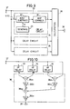
- FIG.9 is a block diagram of a filter circuit, which is an example of an application for the configuration shown in FIGS.5 and 6.
- Delay circuits 33, 34 and 35 each have the same structure as that shown in FIGS.5 and 6.
- the delay circuits 33, 34 and 35 have different delay amounts d x , d y and d z , respectively.
- the delay circuits have their own constant values ⁇ i corresponding to the delay amounts. Different constant values ⁇ i are easily obtainable by changing the combination of high-level inputs and low-level inputs in the constant value generating circuit 23 in each delay circuit.
- the delay circuits 33, 34 and 35 receive an input signal X applied at an input terminal to be filtered.
- the input signal X and output signals of the delay circuits 33, 34 and 35 are supplied to a calculating circuit 36.
- the input signal X is delayed by the delay time d x by the delay circuit 33 and is fed as a signal a to the calculation circuit 36.
- the input signal X is delayed by the delay times d y and d z by the delay circuits 34 and 35, respectively.
- delayed signals b and c from the delay circuits 34 and 35, respectively, are supplied to the calculating circuit 36.
- FIG.10 is a circuit diagram of the calculating circuit 36 shown in FIG.9.
- the signals a and b are applied to an adder 36a1, an output of which is. supplied to a 1/2 level attenuator 36b1.
- An output signal e of the attenuator 36b1 is shown in FIG.11.
- the signal c and the input signal X are supplied to an adder 36a2, an output of which is applied to a 1/2 level attenuator 36b2.
- An output signal f of the attenuator 36b2 is also shown in FIG.11.
- the signals e and f are provided to an adder 36a3, an output of which is fed to a 1/2 attenuator 36b3.
- An output signal Y of the attenuator 36b3 is illustrated in FIG.11. This output signal Y is outputted though an output terminal 38.
- the output signal Y is a substantially sinusoidal waveform. This means that the above odd harmonic components have been eliminated.
- the delay times of the delay circuits 33, 34 and 35 are varied in response to the frequency of the input signal X, and therefore the frequencies of the signal to be filtered follow up the frequency of the input signal X.
- the output signal having a frequency characteristic corresponding to that of the input signal X is obtainable.
- FIG.12 is a block diagram of this embodiment. As described before, the signal processing circuit shown in FIG.5 has only the delay function for the input signal. On the other hand, the configuration shown in FIG.12 has not only the delay function but also a filtering function.
- a constant value generating circuit 43 generates a constant value ⁇ i corresponding to a predetermined delay amount d i .
- An adding circuit 42 adds the constant value ⁇ i to an input signal V i (t) passed through an input terminal 41, for every period which is half of a period of the input signal.
- An amplitude limiting circuit 44 amplitude-limits that output signal of the adding circuit 42 at a level below a maximum level of the output signal by a predetermined level as well as at a level over a minimum level thereof by a predetermined level.
- a direct current (D.C.) level adjusting circuit 45 decreases a D.C. level of an output signal of the amplitude limiting circuit 44, so that the output signal has a D.C. level the same as that of the input signal.
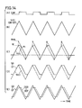
- FIG.13 is a circuit diagram of the configuration shown in FIG.12, and FIGS.14(A) through 14(E) are waveforms at different parts of the circuit shown in FIG.13.
- the input signal V i (t) composed of 8 bits Q0, Q1,..., Q7 are passed through the input terminal 41 and are then fed to the adding circuit 42.
- the input signal V i (t) is a triangular wave signal shown in FIG.14(B).
- the adding circuit 42 includes 4-bit binary full adders 421 and 422 (74-283 type, for example).
- the binary signals Q0 - Q3 are applied to input terminals A1 - A4 of the adder 421, respectively, and the signals Q4 - Q7 are applied to input terminals A1 - A4 of the adder 422, respectively.
- Input terminals B0 - B3 of the adders 421 and 422 receive the constant value ⁇ i derived from the constant value generating circuit 43.
- the constant value generating circuit 43 consists of low-active OR circuits 430 - 437. Each OR circuit is provided with a high-level signal or a low-level signal corresponding to the constant value ⁇ i to be applied to the adding circuit 42.
- the OR circuits also receive a timing signal CAR shown in FIG.14(B) through a terminal 47.
- the timing signal CAR has a period half of the period of the input signal. Therefore, the constant value ⁇ i is produced only when the timing signal CAR is at the high level.
- the outputs of the OR circuits 430 - 433 are supplied to input terminals B1 - B4 of the adder 421, respectively, and the outputs of the OR circuits 434 - 437 are supplied to input terminals B1 - B4 of the adder 422, respectively.
- a low-level signal is always applied to a carry input terminal of the adder 421.
- the adder 421 adds signals between A-side terminals and corresponding B-side terminals and outputs added results through corresponding output terminals E1- E4.
- the adder 422 carries out the adding operation and outputs an adding result between A1 and B1 through output terminals E1- E4.
- the adding circuit 42 When the timing signal CAR is maintained at the low level, the constant value generating circuit 43 does not produce the constant value ⁇ i . Therefore, the adding circuit 42 outputs the binary signals Q0 - Q7 without the added constant value ⁇ i . On the other hand, when the level of the timing signal CAR becomes high, the adding circuit 42 is initiated to add the constant value ⁇ i to the input signal V i (t) composed of the binary signals Q0 - Q7.
- the amplitude limiting circuit 44 shown in FIG.12 has a maximum value limiting circuit 44-1 and a minimum value limiting circuit 44-2, as shown in FIG.13.
- the maximum value limiting circuit 44-1 is composed of 8 OR circuits 44a0 - 44a7.
- the OR circuits 44a0 - 44a3 receive output signals from the terminals E1 - E4 of the adder 421, respectively and the OR circuits 44a4 - 44a7 receive output signals from the terminals E1 -E4 of the adder 422, respectively. Further, all the OR circuits 44a0 - 44a7 receive the carry output of the adder 422.
- the level of the output signal of the maximum value limiting circuit 44-1 is maintained at the maximum value M, as shown in FIG.14(C), so long as the outputs of the adders 421 and 422 correspond to the value indicated by the two-dotted chain lines.
- This circuit 44-2 includes magnitude comparators 44b1 and 44b2 (74-85 type, for example), low-active OR circuits 44c0 - 44c2 and 44c4 - 44c6, OR circuits 44c3 and 44c7, and an inverter 44d, as shown in FIG.13.
- the outputs of the OR circuits 44a0 - 44a3 are fed to input terminals A0 - A3 of the comparator 44b1, and the outputs of the OR circuits 44a4 - 44a7 are supplied to input terminals A0 - A3 of the comparator 44b2.
- Input terminals B0 - B3 of the comparators 44b1 and 44b2 are provided with binary signals corresponding to a reference level L ref shown by a dotted chain line in FIG.14(C).
- the low-level signal is applied to the terminals B0 - B2 of the comparators 44b1 and 44b2, and the high-level signal is applied to the terminals B3 thereof.
- the binary outputs of the OR circuits 44a0 - 44a7 are also supplied to the OR circuits 44c0 - 44c7, respectively.
- the signal from the terminal A ⁇ B of the comparator 44b2 is delivered to the OR circuits 44c3 and 44c7, and further inverted by an inverter 44d and supplied to the OR circuits 44c0 - 44c2, and 44c4 - 44c6.
- the OR circuits 44c0 - 44c7 produce signals corresponding to the reference level L ref .
- the output signals of the amplitude limiting circuit 44 is supplied to the D.C. level adjusting circuit 45.
- This circuit 45 consists of two 4-bit binary full adders 451 and 452 (74-283 type, for example).
- the binary signals S0 - S3 are fed to input terminals A1 - A4 of the adder 451, and the signals S4 - S7 are fed to input terminals A1 - A4 of the adder 452.
- Input terminals B1 - B4 of the adders 451 and 452 are provided with binary signals corresponding to a D.C. level to be shifted towards a lower-level direction.
- the input terminals B1, B2 and B4 of the adders 451 and 452 are provided with the high-level signal, whereas the input terminals B3 thereof are provided with the low-level signal. Since the low-level signal is applied to the carry input terminal C0, the adders act as a subtractor. As a result, binary signals DQ0 - DQ7 indicated by a broken line in FIG.14(E) are outputted through the output terminals 46. It should be noted that the waveform of the output signal shown in FIG.14(E) is substantially the same as those in FIGS.2 and 3.
- the delay time of the output signals DQ0 - DQ7 with respect to the input signals Q0 - Q7 correspond to the constant value ⁇ i . Therefore, it is possible to obtain a desired delay time by suitably selecting the constant value ⁇ i . Further, when the constant value ⁇ i is fixed, the delay time of the output signals varies as a function of the frequency of the input signal. Therefore, the frequency of the signal to be eliminated follows up the frequency of the input signals. As a result, it is possible to obtain the output signal having the frequency characteristic corresponding to the frequency characteristic of the input signal.
- FIGS.12 and 13 has an advantage that it has a filtering function for the input signal.
- the output signal provided by this embodiment (FIG.14(E)) has the waveform substantially identical to the waveforms shown in FIGS.2 and 3.
- FIG.15 is a block diagram of this filter.
- the illustrated filter includes three filter circuits 50, 51 and 52, each of which is the same as the filter shown in FIGS.12 and 13.
- the filter circuits 50, 51 and 52 have different frequencies from each other.
- the filter circuits 50, 51 and 52 have delay times 1/2(d x + 1), 1/2(d y + 1) and 1/2(d z + 1), respectively. These delay times vary with the frequency of an input signal X for the filter, when the constant value ⁇ i is fixed. Of course, the delay times vary by adjusting the constant value ⁇ i .
- Output signals a , b and c of the filter circuits 50, 51 and 52 respectively, are supplied to a calculating circuit 53 together with the input signal X.
- FIG.16 A detailed circuit structure of the calculating circuit 53 is shown in FIG.16.
- the output signals a and b are fed to an adder 53a1, which outputs an added result d .
- These signals are shown in FIG.17.
- the signal d is added to a signal passed through an inverter 53b by an adder 53a2, which outputs an added result e .
- This signal e is added to the output c of the filter circuit 52 by an adder 53a3, which outputs an added result.
- This result is attenuated by a 1/2 level by a level attenuator 53c and applied as an output signal Y to an output terminal 55.
- the output signal Y is a substantially sinusoidal waveform. This means that odd harmonic components have been eliminated from the input triangular wave signal X.
- the present invention is not limited to the embodiments, but various variations and modifications may be made without departing from the scope of the present invention.
- the number of the delay circuits shown in FIG.9 is not limited to three.
- the number of the filter circuits is not limited to three.
- the number of bits to be processed is not limited to 8 bits.
Applications Claiming Priority (8)
| Application Number | Priority Date | Filing Date | Title |
|---|---|---|---|
| JP270094/86 | 1986-11-13 | ||
| JP27009486A JPS63123212A (ja) | 1986-11-13 | 1986-11-13 | 信号処理回路 |
| JP27009286A JPS63123210A (ja) | 1986-11-13 | 1986-11-13 | 信号処理回路 |
| JP270091/86 | 1986-11-13 | ||
| JP27009386A JPS63123211A (ja) | 1986-11-13 | 1986-11-13 | 信号処理回路 |
| JP270093/86 | 1986-11-13 | ||
| JP270092/86 | 1986-11-13 | ||
| JP27009186A JPS63123209A (ja) | 1986-11-13 | 1986-11-13 | 信号処理回路 |
Publications (3)
| Publication Number | Publication Date |
|---|---|
| EP0268532A2 true EP0268532A2 (de) | 1988-05-25 |
| EP0268532A3 EP0268532A3 (en) | 1989-10-25 |
| EP0268532B1 EP0268532B1 (de) | 1995-02-22 |
Family
ID=27478873
Family Applications (1)
| Application Number | Title | Priority Date | Filing Date |
|---|---|---|---|
| EP87402560A Expired - Lifetime EP0268532B1 (de) | 1986-11-13 | 1987-11-12 | Signalverarbeitungseinrichtung |
Country Status (4)
| Country | Link |
|---|---|
| US (1) | US4811260A (de) |
| EP (1) | EP0268532B1 (de) |
| KR (1) | KR900008364B1 (de) |
| DE (1) | DE3751088T2 (de) |
Families Citing this family (7)
| Publication number | Priority date | Publication date | Assignee | Title |
|---|---|---|---|---|
| US5130942A (en) * | 1988-02-24 | 1992-07-14 | Canon Kabushiki Kaisha | Digital filter with front stage division |
| US5212782A (en) * | 1989-01-13 | 1993-05-18 | Vlsi Technology, Inc. | Automated method of inserting pipeline stages in a data path element to achieve a specified operating frequency |
| JPH04502677A (ja) * | 1989-01-13 | 1992-05-14 | ブイエルエスアイ テクノロジー,インコーポレイティド | データパス素子の分析方法 |
| US5133069A (en) * | 1989-01-13 | 1992-07-21 | Vlsi Technology, Inc. | Technique for placement of pipelining stages in multi-stage datapath elements with an automated circuit design system |
| US5033018A (en) * | 1989-04-26 | 1991-07-16 | Hewlett-Packard Company | Filter and method for whitening digitally generated noise |
| US5041998A (en) * | 1989-11-30 | 1991-08-20 | The Grass Valley Group Inc. | Digital video mixer |
| JP3544685B2 (ja) * | 1993-06-14 | 2004-07-21 | 株式会社東芝 | 演算素子結合網 |
Citations (2)
| Publication number | Priority date | Publication date | Assignee | Title |
|---|---|---|---|---|
| JPS554172A (en) * | 1978-06-24 | 1980-01-12 | Nippon Telegr & Teleph Corp <Ntt> | Duplex branching filter device |
| GB2103401A (en) * | 1981-08-06 | 1983-02-16 | Rca Corp | Digital filter circuits |
-
1987
- 1987-11-10 US US07/119,451 patent/US4811260A/en not_active Expired - Lifetime
- 1987-11-12 DE DE3751088T patent/DE3751088T2/de not_active Expired - Fee Related
- 1987-11-12 EP EP87402560A patent/EP0268532B1/de not_active Expired - Lifetime
- 1987-11-13 KR KR1019870012814A patent/KR900008364B1/ko not_active IP Right Cessation
Patent Citations (2)
| Publication number | Priority date | Publication date | Assignee | Title |
|---|---|---|---|---|
| JPS554172A (en) * | 1978-06-24 | 1980-01-12 | Nippon Telegr & Teleph Corp <Ntt> | Duplex branching filter device |
| GB2103401A (en) * | 1981-08-06 | 1983-02-16 | Rca Corp | Digital filter circuits |
Non-Patent Citations (2)
| Title |
|---|
| ELEKTRONIK, vol. 33, no. 1, January 1983, pages 57-64, Munich, DE; C. TIEFENTHALER: "Digitale Transversalfilter" * |
| PATENT ABSTRACTS OF JAPAN, vol. 4, no. 32 (E-2)[514], 19th March 1980, page 42 E 2; & JP-A-55 004 172 (NIPPON DENSHIN DENWA KOSHA) 12-01-1980 * |
Also Published As
| Publication number | Publication date |
|---|---|
| DE3751088D1 (de) | 1995-03-30 |
| DE3751088T2 (de) | 1995-06-14 |
| KR900008364B1 (ko) | 1990-11-17 |
| KR880006841A (ko) | 1988-07-25 |
| US4811260A (en) | 1989-03-07 |
| EP0268532A3 (en) | 1989-10-25 |
| EP0268532B1 (de) | 1995-02-22 |
Similar Documents
| Publication | Publication Date | Title |
|---|---|---|
| US4727506A (en) | Digital scaling circuitry with truncation offset compensation | |
| US4954824A (en) | Sample rate conversion system having interpolation function with phase locked clock | |
| US4982354A (en) | Digital finite impulse response filter and method | |
| CA1193014A (en) | Direct digital to digital sampling rate conversion method and apparatus | |
| US4305133A (en) | Recursive type digital filter | |
| JPH0681012B2 (ja) | デジタル遅延装置 | |
| JPH0681011B2 (ja) | 可変通過帯域フイルタ装置 | |
| EP0450817B1 (de) | Digitale Phasendetektor-Anordnung | |
| EP0268532A2 (de) | Signalverarbeitungseinrichtung | |
| US4580128A (en) | Digital signal processing device | |
| EP0061292B1 (de) | Digital-Analog-Umwandler | |
| KR950008681B1 (ko) | 음질 조절 시스템 | |
| US4755961A (en) | Digital tank circuit | |
| JPH07109974B2 (ja) | ディジタルフィルタ処理装置 | |
| US4634989A (en) | Digital FM detector for a digital signal | |
| EP0107463A1 (de) | Digitales Fernsehsystem mit Fehlerkorrektur | |
| EP0103355B1 (de) | Analog-Digitalwandlungssystem für ein Videosignal | |
| US4642689A (en) | Increasing the resolution of a digitized, time-dependent signal | |
| JPH0421218B2 (de) | ||
| EP0261848B1 (de) | Klangfarbenregelung für bemusterte Daten | |
| US4984187A (en) | First order recursive digital filter without multiplier | |
| CA1182566A (en) | Rate multiplier square root extractor with increased accuracy for transmitter applications | |
| JPS63139492A (ja) | Acc回路 | |
| JPH0365048B2 (de) | ||
| JPH09238048A (ja) | デジタルフィルタ |
Legal Events
| Date | Code | Title | Description |
|---|---|---|---|
| PUAI | Public reference made under article 153(3) epc to a published international application that has entered the european phase |
Free format text: ORIGINAL CODE: 0009012 |
|
| AK | Designated contracting states |
Kind code of ref document: A2 Designated state(s): DE FR GB |
|
| PUAL | Search report despatched |
Free format text: ORIGINAL CODE: 0009013 |
|
| AK | Designated contracting states |
Kind code of ref document: A3 Designated state(s): DE FR GB |
|
| 17P | Request for examination filed |
Effective date: 19900412 |
|
| 17Q | First examination report despatched |
Effective date: 19921015 |
|
| GRAA | (expected) grant |
Free format text: ORIGINAL CODE: 0009210 |
|
| STAA | Information on the status of an ep patent application or granted ep patent |
Free format text: STATUS: THE PATENT HAS BEEN GRANTED |
|
| AK | Designated contracting states |
Kind code of ref document: B1 Designated state(s): DE FR GB |
|
| REF | Corresponds to: |
Ref document number: 3751088 Country of ref document: DE Date of ref document: 19950330 |
|
| ET | Fr: translation filed | ||
| PLBE | No opposition filed within time limit |
Free format text: ORIGINAL CODE: 0009261 |
|
| 26N | No opposition filed | ||
| PGFP | Annual fee paid to national office [announced via postgrant information from national office to epo] |
Ref country code: DE Payment date: 20001106 Year of fee payment: 14 |
|
| PGFP | Annual fee paid to national office [announced via postgrant information from national office to epo] |
Ref country code: GB Payment date: 20001108 Year of fee payment: 14 |
|
| PGFP | Annual fee paid to national office [announced via postgrant information from national office to epo] |
Ref country code: FR Payment date: 20001110 Year of fee payment: 14 |
|
| PG25 | Lapsed in a contracting state [announced via postgrant information from national office to epo] |
Ref country code: GB Free format text: LAPSE BECAUSE OF NON-PAYMENT OF DUE FEES Effective date: 20011112 |
|
| REG | Reference to a national code |
Ref country code: GB Ref legal event code: IF02 |
|
| PG25 | Lapsed in a contracting state [announced via postgrant information from national office to epo] |
Ref country code: DE Free format text: LAPSE BECAUSE OF NON-PAYMENT OF DUE FEES Effective date: 20020702 |
|
| PG25 | Lapsed in a contracting state [announced via postgrant information from national office to epo] |
Ref country code: FR Free format text: LAPSE BECAUSE OF NON-PAYMENT OF DUE FEES Effective date: 20020730 |
|
| REG | Reference to a national code |
Ref country code: FR Ref legal event code: ST |
|
| REG | Reference to a national code |
Ref country code: FR Ref legal event code: ST |