EP0259936B1 - Convertisseur de code à tensions de sortie complémentaires - Google Patents
Convertisseur de code à tensions de sortie complémentaires Download PDFInfo
- Publication number
- EP0259936B1 EP0259936B1 EP87201729A EP87201729A EP0259936B1 EP 0259936 B1 EP0259936 B1 EP 0259936B1 EP 87201729 A EP87201729 A EP 87201729A EP 87201729 A EP87201729 A EP 87201729A EP 0259936 B1 EP0259936 B1 EP 0259936B1
- Authority
- EP
- European Patent Office
- Prior art keywords
- circuit
- flow
- amplifier
- electrode
- signals
- Prior art date
- Legal status (The legal status is an assumption and is not a legal conclusion. Google has not performed a legal analysis and makes no representation as to the accuracy of the status listed.)
- Expired - Lifetime
Links
Images


Classifications
-
- H—ELECTRICITY
- H03—ELECTRONIC CIRCUITRY
- H03M—CODING; DECODING; CODE CONVERSION IN GENERAL
- H03M1/00—Analogue/digital conversion; Digital/analogue conversion
- H03M1/12—Analogue/digital converters
-
- H—ELECTRICITY
- H03—ELECTRONIC CIRCUITRY
- H03M—CODING; DECODING; CODE CONVERSION IN GENERAL
- H03M1/00—Analogue/digital conversion; Digital/analogue conversion
- H03M1/12—Analogue/digital converters
- H03M1/34—Analogue value compared with reference values
- H03M1/36—Analogue value compared with reference values simultaneously only, i.e. parallel type
- H03M1/368—Analogue value compared with reference values simultaneously only, i.e. parallel type having a single comparator per bit, e.g. of the folding type
-
- H—ELECTRICITY
- H03—ELECTRONIC CIRCUITRY
- H03M—CODING; DECODING; CODE CONVERSION IN GENERAL
- H03M1/00—Analogue/digital conversion; Digital/analogue conversion
- H03M1/12—Analogue/digital converters
- H03M1/14—Conversion in steps with each step involving the same or a different conversion means and delivering more than one bit
- H03M1/141—Conversion in steps with each step involving the same or a different conversion means and delivering more than one bit in which at least one step is of the folding type; Folding stages therefore
Definitions
- This invention relates to code converters suitable for use in devices such as analog-to-digital (A/D) converters.
- A/D analog-to-digital
- Parallel converters provide the greatest speed in converting an analog input voltage (generally referred to as "V I ”) into an n-bit digital code.
- V I analog input voltage
- a typical parallel A/D converter such as that described in Nordstrom et al, UK Patent GB-A-1,547,918, or Fujita, EPO Publication EP-A 120,424, has 2 n input comparators for comparing V I with a like number of reference voltages.
- each comparator in Nordstrom et al. employs a pair of NPN transistors whose emitters are tied to a current source. The bases of the pair follow V I and a corresponding one of the reference voltages. The collectors provide complementary signals on a pair of lines connected to respective load elements.
- Each comparator is in one of two states. As V I traverses an input voltage range in one direction, a progressively greater number of the comparators provide outputs representing a particular one of the states.
- a logic network operates on the "thermometer" output supplied by the comparators to generate 2 n circuit signals.
- Each circuit signal is normally logical low and reaches logical high only when V I is in a designated portion of the input range.
- the designated portion for each signal is separate from (i.e., does not overlap) the designated portion for each other signal.
- the designated portions are also spread out at approximately equal intervals across the input range. In this way, all the circuit signals are low at any time except for the one corresponding to the current value of V I .
- a code converter transforms the circuit signals into the digital code which is supplied on n output lines.
- the code converter consists of 2 n NPN transistors. Each has one or more emitters connected selectively to the output lines according to the desired coding.
- the code converter is Fujita is an array of like-polarity field-effect transistors (FET's) whose sources are grounded. The drains of the FET's are selectively connected to the output lines. Since the code converter is Fujita or Nordstrom et al is single ended, a reference must be used to determine whether each bit of the output code is logical low or logical high.
- the main disadvantage of a parallel A/D converter is a high component count due to the large number of input comparators.
- the device requires a large chip area when implemented as an integrated circuit.
- a folding A/D converter contains a coarse parallel A/D converter, a folding circuit, and a fine parallel A/D converter. The coarse converter operates directly on V I to generate the m most significant bits of the digital code.
- the folding circuit contains a set of input amplifiers that compare V I with at least four different reference voltages supplied from a voltage divider.
- the amplifiers are interconnected in such a way as to directly generate one or more pairs of complementary waveforms having a repetitive rounded triangular shape as a function of V I . Extreme values of each waveform occur at V I values dependent on selected ones of the reference voltages.
- the fine converter operates on these waveforms to produce the remaining n-m bits.
- a folding A/D converter utilizes considerably less comparators, including input amplifiers, than an equivalent parallel converter. Chip area is reduced dramatically. However, generation of the repetitive rounded triangular waveforms in the unitary way described above makes the folding converter unduly sensitive to noise. It would be desirable to have a simple technique for overcoming this problem.
- the central feature of this invention is a circuit that converts an input code into an output code consisting of one or more pairs of complementary signals. Due to the double-ended nature of the present code converter, there is no need to use a reference for ascertaining whether each bit of the output code is at a high level or a low level. Accuracy is thus better than that of the single-ended code converters discussed above. Frequency response is also better.
- the code converter is part of an electronic circuit comprising an input section for providing at least three different circuit signals that vary between a high-level value and a low-level value in response to an input parameter that varies across an input range, each circuit signal reaching its high-level value when the input parameter is in a designated portion of the input range separate from the designated portion for each other circuit signal.
- the code converter comprises a current source for providing a substantially constant supply current; two load elements respectively connected to two lines for providing complementary respective signals and at least three like-configured amplifiers respectively corresponding to the circuit signals, each amplifier having a first flow electrode connected to the current source, a second flow electrode, and a control electrode for receiving the corresponding circuit signal so as to cause the path between the first and second flow electrodes to become maximally conductive when the corresponding circuit signal is at its high-level value, charge carriers that move between the flow electrodes of each amplifier originating at its first flow electrode and terminating at its second flow electrode under control of its control electrode, the second flow electrodes being selectively connected to the one or the other of the lines in such a manner that each line is connected to at least one of the second flow electrodes.
- EP-A-0 259 932 which is prior art according to Article 54(3) EPC, discloses a similar electronic circuit. In this circuit, however, the second flow electrodes of the amplifiers are all connected to a DC voltage source and the first flow electrodes of the amplifiers are connected to the lines for providing complementary signals.
- EP-A-0 167 339 discloses a circuit arrangement comprising a current source, two load elements and at least three like-configured amplifiers, interconnected in a similar way.
- the control electrodes are not connected to an input section for providing circuit signals in response to an input parameter in the manner disclosed above.
- the instant code converter is useful in the folding circuit of a folding A/D converter.
- the folding circuit in the present A/D converter utilizes a pair of functionally different portions for generating the repetitive triangular-like waveforms. The division into two portions reduces sensitivity to noise, thereby improving accuracy.
- One of the portions produces three or more circuit signals respectively associated with different pairs of four or more reference voltages.
- the waveform for each circuit signal has a rounded triangular shape that reaches a high-level value when the input voltage is between the associated pair of reference voltages.
- the other portion employs the present code converter for selectively combining these waveforms to produce the repetitive triangular waveforms.
- Fig. 1 is a block diagram of a circuit consisting of an encoder and a double-ended code converter according to the invention.
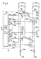
- Fig. 2 is a circuit diagram of an expanded embodiment of the circuit of Fig. 1 in which the encoder produces digital signals;
- Figs. 3a and 3b are graphs of waveforms for certain signals in this embodiment.
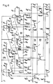
- Fig. 4 is a circuit diagram of an expanded embodiment of the circuit of Fig. 1 in which the encoder produces linear signals;
- Fig. 5 is a graph of the waveforms for certain signals in this embodiment.
- Fig. 6 is a block diagram of a folding A/D converter utilizing the encoding and code converting circuitry of Fig. 4;
- Figs. 7a and 7b are graphs of waveforms for the respective input and output codes of the code converting circuitry.
- Fig. 1 illustrates a circuit containing a code converter 10 which transforms an input code consisting of M+2 circuit voltages V A0 , V A1 ... V AM+1 into an output code consisting of largely complementary main voltages V B and V BN .
- M is 1 or more.
- Voltages V A0 - V AM+1 are often referred to collectively as the "V A " signals.
- voltages V B and V BN are often referred to collectively as the "V B " signals.
- Code converter 10 is formed with M+2 like-configured three-electrode amplifiers T0, T1, ...T M+1 , often referred to collectively as the "T" amplifiers.
- Each amplifier T j (where j runs from 0 to M+1) has a first flow electrode (E1), a second flow electrode (E2), and a control electrode (CE) for controlling current flow between the flow electrodes (E1 and E2). Charge carriers moving between the flow electrodes originate at the first electrode and terminate at the second electrode.
- Each amplifier T j may be embodied with a single transistor.
- its emitter, collector, and base are respectively the first, second, and control electrodes. These are the source, drain, and gate for an FET of either insulated-gate or junction type.
- Amplifier T j could, however, consist of more than a single transistor.
- One example is a bipolar Darlington circuit in which the emitter of an input transistor is connected to the base of a trailing transistor. In this instance, the control electrode is the base of the input transistor, while the first and second flow electrodes are the omitter and collector of the trailing transistor.
- T amplifiers As used in describing the T amplifiers, "like-configured” means that they have corresponding elements interconnected in the same way and that each set of corresponding elements is of the same semiconductor polarity.
- the T amplifiers would generally be “like-configured” if they all are NPN transistors (even though of differing sizes), but not if some are NPN transistors while others are PNP devices.
- Darlington circuits are “like-configured” as long as the input transistors are of the same polarity and the trailing transistors are of the same polarity (even if different from that of the input transistors).
- Voltages V A0 - V AM+1 are respectively supplied as input signals to the control electrodes of amplifiers T0 - T M+1 .
- Their first electrodes are all connected to a circuit supply 12 which may be a current source or a voltage supply.
- the second electrodes of selected ones of the T amplifiers are connected to an output line L B which is connected to a load element 14 B to provide voltage V B .
- the second electrodes of the remainder are connected to an output line L BN which is similarly connected to a load element 14 BN to provide voltage V BN .
- the particular connections of the second electrodes depend on the desired output code.
- Each voltage V Aj varies between a low-level value and a high-level value.
- the adjectives "low-level” and “high-level” are used to distinguish two different signal levels.
- the actual voltage of the "high-level” value may be greater than or less than that of the "low-level” value, depending on the internal characterisitics of the T amplifiers.
- the low-level and high-level values are respectively referred to as “0" and "1".
- the input code is normally chosen such that only one of the V A signals is at "1" at any time, the remainder all being at "0".
- only one of the T amplifiers is maximally conductive at any time.
- the maximally conductive amplifier draws current through the particular line L B or L BN connected to its second electrode. This pulls the corresponding main signal V B or V BN to a low-level value also referred to here as "0".
- the remainder of the T amplifiers are all turned off so that no current flows through the other line L BN or L B .
- the other main signal V BN or V B is at a high-level value again denoted as "1".
- V B and V BN are complementary because their sum is "1".
- Each of a pair of the V A signals may lie between “0" and “1” such that the sum of the two signals is “1". The remainder of the V A signals are all at "0".
- the corresponding pair of the T amplifiers are partially conductive. The pair form a differential device operating in its "linear" range. If the second electrodes of both of the partially conductive amplifiers are connected to the same line L B or L BN , it conducts current to pull the corresponding signal V B or V BN to "0". No current flows through the other line L BN or L B . Its signal V BN or V B is at "1".
- V B and V BN lie between “0" and "1". Their actual values depend on the relative values of the two "non-zero" V Aj signals. The sum of V B and V BN is, however, still "1".
- V B and V BN there are several further limitations which usually must be satisfied for V B and V BN to be complementary. If supply 12 is a current source that provides a substantially constant supply current, the sum of V B and V BN is fixed by the supply current. The current source therefore should be fully conductive. Otherwise, the sum of V B and V BN will differ from "1" because insufficient current flows through lines L B and L BN .
- the T amplifiers normally need not be identical. However, they should be identical if supply 12 is a voltage supply, particularly when they are embodied with FET"s.
- An input encoder 16 generates the V A signals in response to an input parameter which varies across an input range.
- the input parameter is denoted generally as "V I ".
- Encoder 16 preferably sets each signal V Aj at "1" only when V I is in a single portion of the input range. This portion is separate from the portions of the input range where the other V A signals reach "1".
- Fig. 2 shows an expanded version of Fig. 1 in which the V A signals are "digital" signals.
- the circuit of Fig. 2 contains two code converters 10 X and 10 Y . Each is a bipolar embodiment of converter 10 for which M is at least 2. Converters 10 X and 10 Y receive the same V A input code but have different second electrode (collector) connections so as to produce different V B output codes.
- each amplifier T j of Fig. 1 is an NPN transistor Q j in Fig. 2.
- Supply 12 is a current source I B that provides a substantially constant supply current.
- Each load element 14 B or 14 BN is a load resistor R L . Terminals V CC and V EE respectively provide high and low supply voltages.
- Input encoder 16 in Fig. 2 consists of a thermometer encoder 18 and M logical AND gates G1 - G M .
- encoder 18 In response to parameter V I , encoder 18 generates M+1 digital signals S1 - S M+1 that have a "thermometer" variation of the type indicated in Fig. 3a.
- V I moves in the positive direction through the input range here indicated as extending from 0 to M+1, each signal S j switches in sequence from logical "0" to logical "1". The S j transitions are very sharp.
- Encoder 18 also generates the respective digital complements S N1 - S NM+1 of signals S1 - S M+1 .
- each gate G j For j running from 1 to M, each gate G j logically "AND's" signals S j and S Nj+1 to produce voltage V Aj .
- V A0 and V AM+1 are supplied directly as signals S N1 and S M+1 .
- Fig. 3b illustrates how the V A signals vary as a function of V I . Except for V A0 and AM+1 , each V Aj waveform sequentially rises sharply from “0” to “1", stays at “1” for a specified interval which is largely the same for all of waveforms V A1 - V AM , and falls sharply to "0” as the next signal V Aj+1 rises from “0” to “1".
- Fig. 3b also shows the resulting waveforms for signals V BX and V BNX for the particular collector connections depicted in Fig. 2 for converter 10 X .
- Fig. 4 illustrates an expanded version of Fig. 1 in which the V A signals are "linear" signals.
- the circuit of Fig. 4 contains an array 20 consisting of P code converters 101 - 10 P .
- Each converter 10 k (where k runs from 1 to P) is an embodiment of converter 10 utilizing the same elements as converter 10 X or 10 Y of Fig. 2.
- Converters 101 - 10 P have the same second electrode (collector) connections relative to one another but receive different V A input codes and thereby produce different V B output codes.
- an input amplifier circuit 22 operates on parameter V I , which is here an analog input voltage, to produce the V A signals.
- Circuit 22 is formed with a resistive voltage divider 24 and an array 26 consisting of P groups 261 - 26 P of differential amplifiers A jk .
- divider 24 consists of (M+1)P-1 resistors R D connected in series between low voltage V R11 and high voltage V RM+1P . Including these two voltages, divider 24 provides amplifier array 26 with (M+1)P reference voltages V R11 - V R1P ...V RM+11 .
- Each amplifier group 26 k consists of M+1 amplifiers A 1k - A M+1k that jointly provide M+2 voltages V A0k - V AM+1k to respective transistors Q 0k - Q M+1k in converter 10 k - V RM+1P .
- Each amplifier 26 k in combination with divider 24 is thus an embodiment of encoder 16.
- Each amplifier A jk amplifies the difference between voltages V I and V Rjk .
- the core of amplifier A jk is a pair of NPN transistors Q L and Q R whose emitters are connected to a constant current source I EE Voltages V I and V Rjk are supplied to the bases of transistors Q L and Q R . Their collectors are connected to respective load resistors R C .
- the non-inverted output of amplifier A jk would normally be available at the Q R collector.
- the Q L collector would normally provide the inverted (or complementary) output.
- each signal V Ajk is taken from a connection of the Q R collector in amplifier A jk to the Q L collector in amplifier A j+1k . This acts to "linearly AND" the non-inverted A jk output and the inverted A j+1k output.
- Components 24 and 26 k thus perform a "linear" function similar to the "digital" function performed by components 18 and G1 - G M in Fig. 2.
- Fig. 5 generally illustrates how V A0 - V AM+1k vary with V I . Except for voltages V A0k and V AM+1k , each voltage V Ajk sequentially rises from “0" to “1” in a transition portion of the input range centered around V Rjk , stays at “1” in a main portion of the V I range extending from slightly above V Rjk to slightly below V Rj+1k , and then falls to "0" in another transition portion centered around V Rj+1k as the next voltage V Aj+1k rises from “0" to "1". Voltages V A0k and V AM+1k , which each make only a single transition, respectively account for underflow and overflow.
- Each transistor Q jk becomes progressively more conductive as its input voltage V jk moves from “0" to “1” and vice versa.
- the transitions in V A0k - V AM+1k are thereby reflected in V Bk and V BNk as shown in Fig. 5.
- Resistors R D preferably all have the same value. Consequently, the "main" portions of the V I range all have approximately the same pulse width and are spread out at approximately equal intervals from one another. By suitably adjusting the R D values, each main portion can be compressed to a single point.
- Fig. 6 illustrates an application of the encoding and code converting circuitry of Fig. 4 to an A/D converter of the multiple-folding type.
- This device converts analog voltage V I into an 8-bit digital code. M and P are both 8 here.
- the input section to the A/D converter is circuit 22 in which divider 24 provides 72 reference voltages V R11 - V R98 .
- Amplifier array 26 in circuit 22 compares V I with each of V R11 - V R98 to produce 80 circuit voltages V A01 - V A98 .
- Components 20 and 22 may include some additional circuitry to assure that the V A signals produce the necessary shapes for the V B signals at the low and high ends of the V I range.
- FIG. 7a illustrates the general shape for V Ajk as a function of V I .
- Each V Ajk waveform would ideally have the triangular shape shown in dashed line. Due to practical amplifier characteristics, V Ajk varies according to the more rounded shape indicated in solid line. V Ajk reaches a maximum when V I is approximately half way between V Rjk and V Rj+1k .
- Circuit 20 here acting as a folding array, electrically combines selected V A signals in the manner described above to generate 8 voltages C B1 - V B8 and their complements V BN1 - V BN8 .
- Fig. 7b depicts part of the resulting V B waveforms.
- V B1 is shown in thicker line.
- the remaining waveforms have the same shape and spacing as those illustrated. Due to the roundings of the tips of the V A waveforms, each V B waveform has a repetitive rounded triangular shape.
- Each voltage V Bk or V BNk reaches extreme values when V I is approximately halfway between each pair of voltages V Rjk and V Rj+1k .
- an interpolation circuit 28 interpolates by a factor of 4 between each pair of consecutive V B signals to generate 32 interpolated signals V B1 - V B32 and their complements V NB1 - V NB32 .
- a group of comparators 30 compares V B1 - V B32 respectively with V NB1 - V NB32 to produce a string of 32 bits D1 - D32.
- a code converter 32 which may be conventional or may follow the teachings of this invention, converts the bit string into the five least significant bits MSB-3 -- MSB-7 of the digital code.
- the final part of the A/D converter is a group of comparators 34 which generate the three most significant bits MSB -- MSB-2 in response to three pairs of substantially complementary further signals V C .
- Fig. 6 indicates that array 20 provides the V C signals.
Claims (10)
- Circuit électronique comportant une partie d'entrée (16) pour délivrer au moins trois signaux de circuit différents (VA0..VAM+1) variant entre une valeur de niveau haut et une valeur de niveau bas en réaction à un paramètre d'entrée (VI) variant sur une gamme d'entrée, chaque signal de circuit (VA0..VAM+1) atteignant sa valeur de niveau haut lorsque le paramètre d'entrée (VI) se situe dans une partie désignée de la gamme d'entrée, séparée de la partie désignée pour chaque autre signal de circuit (VA0..VAM+1) caractérisé en ce qu'il comporte en outre:
une source de courant (12) pour fournir un courant d'alimentation sensiblement constant,
deux éléments de charge (14B, 14BN) reliés respectivement à deux lignes (LB, LBN) pour fournir des signaux respectifs complémentaires (VB, VBN) et
au moins trois amplificateurs de configuration similaire (T₀..TM+1) correspondant respectivement aux signaux de circuit (VA0..VAM+1) chaque amplifieateur présentant une première électrode de courant (E1) reliée à la source de courant (12), une seconde électrode de courant (E2) et une électrode de commande (CE) pour recevoir le signal de circuit correspondant (VA0..VAM+1) pour faire en sorte que le trajet entre les première (E1) et seconde (E2) électrodes de courant devienne conducteur au degré maximal lorsque le signal de circuit correspondant (VA0..VAM+1) est à sa valeur de niveau élevé, des porteurs de charge se déplaçant entre les électrodes de courant de chaque amplificateur partant de sa première électrode de courant (E1) et aboutissant à sa seconde électrode de courant (E2) sous la commande de son électrode de commande (CE), les secondes électrodes de courant étant reliées de façon sélective à l'une ou à l'autre des lignes (LB, LBN) de façon que chaque ligne soit reliée à au moins l'une des secondes électrodes de courant. - Circuit selon la revendication 1, caractérisé a ce que chaque amplificateur (T₀..TM+1) comporte un transistor bipolaire ayant un émetteur, un collecteur et une base constituant respectivement les première et seconde électrodes de courant et l'électrode de commande de cet amplificateur.
- Circuit selon la revendication 1, caractérisé en ce que chaque amplificateur (T₀..TM+1) comporte un transistor à effet de champ ayant une source, un drain et une grille constituant respectivement les première et seconde électrodes de courant et l'électrode de commande de cet amplificateur.
- Circuit selon la revendication 1, 2 ou 3, caractérisé en ce que les signaux de circuit (VA0..VAM+1) sont des signaux numériques, chaque amplificateur (T₀..TM+1) étant bloqué lorsque le signal de circuit correspondant (VA0..VAM+1) est à sa valeur de niveau bas, un seul des signaux de circuit (VA0..VAM+1) étant à sa valeur de niveau haut à n'importe quel instant, de sorte que, un seul des amplificateurs T₀..TM+1) est effectivement conducteur à n'importe quel instant.
- Circuit selon la revendication 1, 2 ou 3, caractérisé en ce que les signaux de circuit (VA0..VAM+1) sont des signaux linéaires, chaque amplificateur (T₀..TM+1) étant bloqué lorsque le signal de circuit correspondant (VA0..VAM+1) est à sa valeur de niveau bas et devenant progressivement plus conducteur lorsque le signal de circuit correspondant (VA0..VAM+1) va à sa valeur de niveau haut, chaque signal allant à sa valeur de niveau bas lorsque le paramètre d'entrée (VI) traverse chacune d'une paire de parties de transition placées de part et d'autre de la partie désignée de la gamme d'entrée pour ce signal de circuit, chaque partie de transition, à l'exception des deux parties de transition les plus distantes, chevauchant précisément sur l'une des autres parties de transition, de sorte que deux des amplificateurs peuvent être simultanément conducteurs.
- Circuit selon la revendication 1, 2, 3, 4 ou 5, caractérisé en ce que les parties désignées sont réparties sur la gamme d'entrée à des intervalles sensiblement égaux.
- Circuit selon la revendication 1, 2, 3, 4, 5 ou 6, caractérisé en ce que la partie d'entrée fournit un quatrième signal de circuit (VA0..VAM+1) variant entre une valeur de niveau haut et une valeur de niveau bas en réaction au paramètre d'entrée (VI), le quatrième signal de circuit atteignant sa valeur de niveau haut lorsque le paramètre d'entrée (VI) se situe dans une partie désignée de la gamme d'entrée, séparée des autres parties désignées, et en ce que le circuit électronique comporte en outre un quatrième amplificateur de configuration similaire (T₀..TM+1) ayant une première électrode de courant (E1) reliée à la source de courant (12), une seconde électrode de courant (E2) reliée à l'une choisie des lignes (LB, LBN) et une électrode de commande (CE) pour recevoir le quatrième signal de circuit pour faire en sorte que le quatrième amplificateur (T₀..TM+1) devient conducteur au degré maximal lorsque le quatrième signal de circuit (VA0..VAM+1) atteint sa valeur de niveau haut, des porteurs de charge se déplaçant entre les électrodes de courant du quatrième amplificateur partant de sa première électrode de courant (E1) et aboutissant à sa seconde électrode de courant (E2) sous la commande de son électrode de commande (CE).
- Circuit selon la revendication 1, caractérisé en ce qu'il comporte en outre:
une autre source de courant (IBY) pour fournir un courant d'alimentation sensiblement constant;
deux autres éléments de charge (RL) reliés respectivement à deux autres lignes (LBY, LBNY) pour fournir des signaux respectifs complémentaires (VBY, VBNY) et
au moins trois autres amplificateurs de configuration similaire (Q0Y..QM+1Y) correspondant respectivement aux signaux de circuit (VA0..VAM+1), chaque autre amplificateur ayant une première électrode de courant reliée à l'autre source de courant (IBY), une seconde électrode de courant et une électrode de commande pour recevoir le signal de circuit correspondant (VA0..VAM+1) pour faire en sorte que l'amplificateur devienne conducteur au degré maximal lorsque le signal de circuit correspondant est à sa valeur de niveau haut, des porteurs de charge se déplaçant entre les électrodes de courant de chaque autre amplificateur (Q0Y..QM+1Y) partant de sa première électrode de courant et aboutissant à sa seconde électrode de courant sous la commande de son électrode de commande, les secondes électrodes de courant des autres amplificateurs (Q0Y..QM+1Y) étant reliées de façon sélective à l'une ou à l'autre des autres lignes (LBY, LBNY), de telle manière que chaque autre ligne soit reliée au moins à l'une de ces secondes électrodes de courant. - Convertisseur analogique-numérique pour convertir une tension d'entrée analogique (VI) variant sur une gamme d'entrée en un code numérique (MSB..MSB-7), comportant des moyens de référence (24) pour fournir au moins quatre tensions de référence différentes (VR11..VRIP..VRM+11..VRM+1P) réparties sur la gamme d'entrée, des moyens (22, 20) servant, en réaction aux tensions d'entrée (VI) et de référence (VR11..VRIP..VRM+11..VRM+1P), à engendrer au moins une paire de signaux principaux sensiblement complémentaires (VB1 - VB8, VBN1 - VBN8, VC), la forme d'onde de la tension pour chaque signal principal en fonction de la tension d'entrée étant de forme triangulaire arrondie répétitive avec des valeurs extrêmes apparaissant a des valeurs de la tension d'entrée dépendantes de tensions choisies des tensions de référence; et des moyens (34, 28, 30, 32) pour travailler sur les signaux principaux (VB1 - VB8, VBN1 - VBN8, VC), afin d'engendrer au moins une partie du code numérique (MSB-3 ..MSB-7, MSB..MSB-2), caractérisé en ce que les moyens de génération (20, 22) comportent:
une partie d'entrée (A₁₁..AM+1P) pour fournir trois signaux de circuit (VA01..VAM+1P) respectivement associés à différentes paires de tensions de référence (VR11..VRIP..VRM+11..VRM+1P), la forme d'onde pour chaque signal de circuit VAjk) en fonction du signal d'entrée (VI) étant de forme triangulaire arrondie, atteignant une valeur de niveau haut lorsque la tension d'entrée est à une valeur déterminée entre la paire associée de tension de référence (VRik, VRj+1k) et allant à une valeur de niveau bas lorsque la tension d'entrée s'éloigne de la valeur déterminée; et
au moins un convertisseur de signaux (10₁ ..10P) comportant chacun:
une source de courant (IB1..IBP) pour fournir un courant d'alimentation sensiblement constant,
deux éléments de charge (RL) respectivement reliés à deux lignes (LB1, LBN1..LBP, LBNP); et
au moins trois amplificateurs de configuration similaire (Q₀₁..QM+1P), correspondant respectivement aux signaux de circuit (VA01..VAM+1P), chaque amplificateur ayant une première électrode de courant, une seconde électrode de courant et une électrode de commande pour recevoir le signal de circuit correspondant, des porteurs de charge se déplaçant entre les électrodes de courant de chaque amplificateur partant de sa première électrode de courant et aboutissant à sa seconde électrode de courant sous la commande de son électrode de commande, les premières électrodes de courant de chaque amplificateur (Q₀₁, Q₁₁..QM+11), étant reliées à la source de courant (IB1), les secondes électrodes des amplificateurs (Q₀₁, Q₁₁, QM+11) étant reliées de façon sélective à l'une (LBN1) ou l'autre (LB1) des lignes de façon que chaque ligne soit reliée à la seconde électrode d'au moins l'un des amplificateurs spécifiés, les lignes (LB1, LBN1) fournissant une paire des signaux principaux sensiblement complémentaires (VB1, VBN1). - Convertisseur analogique-numérique selon la revendication 9, caractérisé en ce que chaque amplificateur est un transistor bipolaire ayant un émetteur, un collecteur et une base constituant respectivement la première électrode de courant la seconde électrode de courant et l'électrode de commande de cet amplificateur.
Applications Claiming Priority (2)
| Application Number | Priority Date | Filing Date | Title |
|---|---|---|---|
| US06/907,349 US4737766A (en) | 1986-09-12 | 1986-09-12 | Code converter with complementary output voltages |
| US907349 | 1992-07-01 |
Publications (3)
| Publication Number | Publication Date |
|---|---|
| EP0259936A2 EP0259936A2 (fr) | 1988-03-16 |
| EP0259936A3 EP0259936A3 (en) | 1990-07-11 |
| EP0259936B1 true EP0259936B1 (fr) | 1993-12-29 |
Family
ID=25423940
Family Applications (1)
| Application Number | Title | Priority Date | Filing Date |
|---|---|---|---|
| EP87201729A Expired - Lifetime EP0259936B1 (fr) | 1986-09-12 | 1987-09-10 | Convertisseur de code à tensions de sortie complémentaires |
Country Status (5)
| Country | Link |
|---|---|
| US (1) | US4737766A (fr) |
| EP (1) | EP0259936B1 (fr) |
| JP (1) | JPS63132529A (fr) |
| KR (1) | KR950010210B1 (fr) |
| DE (1) | DE3788611T2 (fr) |
Families Citing this family (5)
| Publication number | Priority date | Publication date | Assignee | Title |
|---|---|---|---|---|
| US4897656A (en) * | 1985-12-16 | 1990-01-30 | North American Philips Corporation, Signetics Division | Complementary voltage interpolation circuit with transmission delay compensation |
| NL8701816A (nl) * | 1987-08-03 | 1989-03-01 | Philips Nv | Elektrische schakeling die gebruikt kan worden in een a/d-omzetter. |
| GB9205727D0 (en) * | 1992-03-16 | 1992-04-29 | Sarnoff David Res Center | Averaging,flash analog to digital converter |
| US5489905A (en) * | 1993-12-08 | 1996-02-06 | At&T Corp. | Merged decoding circuit for analog-to-digital flash conversion |
| US5706008A (en) * | 1996-03-01 | 1998-01-06 | Analog Devices, Inc. | High bandwidth parallel analog-to-digital converter |
Family Cites Families (7)
| Publication number | Priority date | Publication date | Assignee | Title |
|---|---|---|---|---|
| DE1230079B (de) * | 1964-04-30 | 1966-12-08 | Motorola Inc | Bistabiler Multivibrator mit Emitteranzapfung |
| CA1105143A (fr) * | 1976-02-12 | 1981-07-14 | Robert A. Nordstrom | Traduction non-disponible |
| US4386339A (en) * | 1980-03-31 | 1983-05-31 | Hewlett-Packard Company | Direct flash analog-to-digital converter and method |
| JPS59171315A (ja) * | 1983-03-18 | 1984-09-27 | Nec Corp | アナログ−デジタル変換器 |
| JPH0773208B2 (ja) * | 1984-06-30 | 1995-08-02 | ソニー株式会社 | 論理回路 |
| US4591830A (en) * | 1984-11-15 | 1986-05-27 | Motorola, Inc. | Comparator cell for analog-to-digital flash converter |
| NL8602294A (nl) * | 1986-09-11 | 1988-04-05 | Philips Nv | Elektronische schakeling met complementair signaalvoerende gegevenslijnen. |
-
1986
- 1986-09-12 US US06/907,349 patent/US4737766A/en not_active Expired - Fee Related
-
1987
- 1987-09-10 DE DE3788611T patent/DE3788611T2/de not_active Expired - Fee Related
- 1987-09-10 EP EP87201729A patent/EP0259936B1/fr not_active Expired - Lifetime
- 1987-09-11 JP JP62228240A patent/JPS63132529A/ja active Pending
- 1987-09-11 KR KR1019870010108A patent/KR950010210B1/ko active IP Right Grant
Also Published As
| Publication number | Publication date |
|---|---|
| JPS63132529A (ja) | 1988-06-04 |
| DE3788611D1 (de) | 1994-02-10 |
| US4737766A (en) | 1988-04-12 |
| EP0259936A3 (en) | 1990-07-11 |
| KR950010210B1 (ko) | 1995-09-11 |
| DE3788611T2 (de) | 1994-06-30 |
| KR880004649A (ko) | 1988-06-07 |
| EP0259936A2 (fr) | 1988-03-16 |
Similar Documents
| Publication | Publication Date | Title |
|---|---|---|
| EP0227165B1 (fr) | Circuit d'interpolation entre tensions complémentaires | |
| US4928103A (en) | Parallel analog-to-digital converter using 2.sup.(n-1) comparators | |
| EP0319097B1 (fr) | Circuit d'interpolation de tension complémentaire à compensation de retard de transmission | |
| US5184130A (en) | Multi-stage A/D converter | |
| US5436629A (en) | Multi-stage A/D converter | |
| US5194867A (en) | Flash analog-to-digital converter employing least significant bit-representative comparative reference voltage | |
| US5640163A (en) | Folding stage and folding analog-to-digital converter | |
| EP0259936B1 (fr) | Convertisseur de code à tensions de sortie complémentaires | |
| US4393368A (en) | Multithreshold A/D converter utilizing error amplifiers | |
| US4306224A (en) | Analog-to-digital converting apparatus | |
| US6411246B2 (en) | Folding circuit and A/D converter | |
| US5633638A (en) | Folding stage for a folding analog-to-digital converter | |
| US4591830A (en) | Comparator cell for analog-to-digital flash converter | |
| US4939517A (en) | Circuit for synchronizing transitions of bits in a digital code | |
| US5181035A (en) | Interpolation analog/digital converter | |
| US6798370B1 (en) | Parallel A/D converter | |
| JPH09167965A (ja) | 基準電圧発生回路 | |
| US20040061636A1 (en) | Analog-to-digital converter and method for converting an analog signal into a digital signal | |
| US6445221B1 (en) | Input driver for a differential folder employing a static reference ladder | |
| EP0121234B1 (fr) | Décodeur pour convertisseur N/A | |
| US4864304A (en) | Analog voltage signal comparator circuit | |
| KR0162633B1 (ko) | 아날로그-디지탈 변환기 | |
| KR100282443B1 (ko) | 디지탈/아날로그 컨버터 | |
| KR100490122B1 (ko) | 폴딩-인터폴레이팅 아날로그-디지털 변환기 | |
| US4647904A (en) | Folding-type analog-to-digital converter |
Legal Events
| Date | Code | Title | Description |
|---|---|---|---|
| PUAI | Public reference made under article 153(3) epc to a published international application that has entered the european phase |
Free format text: ORIGINAL CODE: 0009012 |
|
| AK | Designated contracting states |
Kind code of ref document: A2 Designated state(s): DE FR GB IT NL |
|
| PUAL | Search report despatched |
Free format text: ORIGINAL CODE: 0009013 |
|
| RHK1 | Main classification (correction) |
Ipc: H03M 1/36 |
|
| AK | Designated contracting states |
Kind code of ref document: A3 Designated state(s): DE FR GB IT NL |
|
| 17P | Request for examination filed |
Effective date: 19901219 |
|
| 17Q | First examination report despatched |
Effective date: 19920601 |
|
| GRAA | (expected) grant |
Free format text: ORIGINAL CODE: 0009210 |
|
| AK | Designated contracting states |
Kind code of ref document: B1 Designated state(s): DE FR GB IT NL |
|
| PG25 | Lapsed in a contracting state [announced via postgrant information from national office to epo] |
Ref country code: NL Effective date: 19931229 |
|
| REF | Corresponds to: |
Ref document number: 3788611 Country of ref document: DE Date of ref document: 19940210 |
|
| ITF | It: translation for a ep patent filed |
Owner name: ING. C. GREGORJ S.P.A. |
|
| ET | Fr: translation filed | ||
| NLV1 | Nl: lapsed or annulled due to failure to fulfill the requirements of art. 29p and 29m of the patents act | ||
| PGFP | Annual fee paid to national office [announced via postgrant information from national office to epo] |
Ref country code: GB Payment date: 19940901 Year of fee payment: 8 |
|
| PGFP | Annual fee paid to national office [announced via postgrant information from national office to epo] |
Ref country code: FR Payment date: 19940928 Year of fee payment: 8 |
|
| PLBE | No opposition filed within time limit |
Free format text: ORIGINAL CODE: 0009261 |
|
| STAA | Information on the status of an ep patent application or granted ep patent |
Free format text: STATUS: NO OPPOSITION FILED WITHIN TIME LIMIT |
|
| PGFP | Annual fee paid to national office [announced via postgrant information from national office to epo] |
Ref country code: DE Payment date: 19941125 Year of fee payment: 8 |
|
| 26N | No opposition filed | ||
| ITPR | It: changes in ownership of a european patent |
Owner name: CAMBIO RAGIONE SOCIALE;PHILIPS ELECTRONICS N.V. |
|
| REG | Reference to a national code |
Ref country code: FR Ref legal event code: CD |
|
| PG25 | Lapsed in a contracting state [announced via postgrant information from national office to epo] |
Ref country code: GB Effective date: 19950910 |
|
| GBPC | Gb: european patent ceased through non-payment of renewal fee |
Effective date: 19950910 |
|
| PG25 | Lapsed in a contracting state [announced via postgrant information from national office to epo] |
Ref country code: FR Effective date: 19960531 |
|
| PG25 | Lapsed in a contracting state [announced via postgrant information from national office to epo] |
Ref country code: DE Effective date: 19960601 |
|
| REG | Reference to a national code |
Ref country code: FR Ref legal event code: ST |
|
| PG25 | Lapsed in a contracting state [announced via postgrant information from national office to epo] |
Ref country code: IT Free format text: LAPSE BECAUSE OF NON-PAYMENT OF DUE FEES;WARNING: LAPSES OF ITALIAN PATENTS WITH EFFECTIVE DATE BEFORE 2007 MAY HAVE OCCURRED AT ANY TIME BEFORE 2007. THE CORRECT EFFECTIVE DATE MAY BE DIFFERENT FROM THE ONE RECORDED. Effective date: 20050910 |