EP0259026A2 - Doppelheterostruktur-Halbleiterlaser mit streifenförmigem Mesa-Wellenleiter - Google Patents
Doppelheterostruktur-Halbleiterlaser mit streifenförmigem Mesa-Wellenleiter Download PDFInfo
- Publication number
- EP0259026A2 EP0259026A2 EP87307041A EP87307041A EP0259026A2 EP 0259026 A2 EP0259026 A2 EP 0259026A2 EP 87307041 A EP87307041 A EP 87307041A EP 87307041 A EP87307041 A EP 87307041A EP 0259026 A2 EP0259026 A2 EP 0259026A2
- Authority
- EP
- European Patent Office
- Prior art keywords
- layer
- cladding layer
- semiconductor laser
- semiconductor
- group element
- Prior art date
- Legal status (The legal status is an assumption and is not a legal conclusion. Google has not performed a legal analysis and makes no representation as to the accuracy of the status listed.)
- Granted
Links
Images

Classifications
-
- H—ELECTRICITY
- H01—ELECTRIC ELEMENTS
- H01S—DEVICES USING THE PROCESS OF LIGHT AMPLIFICATION BY STIMULATED EMISSION OF RADIATION [LASER] TO AMPLIFY OR GENERATE LIGHT; DEVICES USING STIMULATED EMISSION OF ELECTROMAGNETIC RADIATION IN WAVE RANGES OTHER THAN OPTICAL
- H01S5/00—Semiconductor lasers
- H01S5/20—Structure or shape of the semiconductor body to guide the optical wave ; Confining structures perpendicular to the optical axis, e.g. index or gain guiding, stripe geometry, broad area lasers, gain tailoring, transverse or lateral reflectors, special cladding structures, MQW barrier reflection layers
- H01S5/22—Structure or shape of the semiconductor body to guide the optical wave ; Confining structures perpendicular to the optical axis, e.g. index or gain guiding, stripe geometry, broad area lasers, gain tailoring, transverse or lateral reflectors, special cladding structures, MQW barrier reflection layers having a ridge or stripe structure
- H01S5/223—Buried stripe structure
- H01S5/2231—Buried stripe structure with inner confining structure only between the active layer and the upper electrode
-
- H—ELECTRICITY
- H01—ELECTRIC ELEMENTS
- H01S—DEVICES USING THE PROCESS OF LIGHT AMPLIFICATION BY STIMULATED EMISSION OF RADIATION [LASER] TO AMPLIFY OR GENERATE LIGHT; DEVICES USING STIMULATED EMISSION OF ELECTROMAGNETIC RADIATION IN WAVE RANGES OTHER THAN OPTICAL
- H01S5/00—Semiconductor lasers
- H01S5/30—Structure or shape of the active region; Materials used for the active region
- H01S5/32—Structure or shape of the active region; Materials used for the active region comprising PN junctions, e.g. hetero- or double- heterostructures
- H01S5/323—Structure or shape of the active region; Materials used for the active region comprising PN junctions, e.g. hetero- or double- heterostructures in AIIIBV compounds, e.g. AlGaAs-laser, InP-based laser
- H01S5/32308—Structure or shape of the active region; Materials used for the active region comprising PN junctions, e.g. hetero- or double- heterostructures in AIIIBV compounds, e.g. AlGaAs-laser, InP-based laser emitting light at a wavelength less than 900 nm
- H01S5/32325—Structure or shape of the active region; Materials used for the active region comprising PN junctions, e.g. hetero- or double- heterostructures in AIIIBV compounds, e.g. AlGaAs-laser, InP-based laser emitting light at a wavelength less than 900 nm red laser based on InGaP
Definitions
- the present invention relates to a double-heterostructure semiconductor laser, and, more particularly, to a semiconductor laser with a mesa stripe waveguide structure which continuously produces light beams at the ambient temperature in a fundamental transverse-oscillation mode.
- the co-pending United States Patent Application Serial No. 019,332 filed February 26, 1987 proposes a double-heterostructure semiconductor laser, which is fabricated on a GaAs substrate by the MOCVD method and has cladding layers formed of InGaAlp -- a new semiconductor material for a laser.
- a p conductivity type InGaAlp cladding layer is formed to have a mesa stripe shape defined by two slanted side surfaces.
- the cladding layer therefore provides a linear projection or rib which defines the mesa-like waveguide channel section of a semiconductor laser.
- Current-blocking layers of an n conductivity type are provided to partially cover the mesa stripe-shaped cladding layer, and perform current-blocking function for the laser in a visible laser beam emission mode. It is desirable for the cladding layer that the band gap and the hole mobility within the cladding layer are as large as possible.
- the composition ratio is typically selected to provide a direct transitional band gap.
- the aluminium composition ratio y of the InGaAlP cladding layer is selected to be y ⁇ 0.35.
- the cladding layer is in an indirect transition stage so that an increase in the band gap of this layer becomes significantly gentle and the hole mobility in the cladding layer is reduced. This is not desirable for a laser which uses a pn junction to provide the current-blocking function.
- the semiconductor laser with the above structure it is likely to cause a lattice defect at the boudary between the cladding layer and the current-blocking layers (particularly, the boundary at the slanted portions of the mesa stripe-shaped channel).
- the lattice defect causes current to leak at the pn junction.
- the leak current increases in the forward-bias or reverse-bias direction during emission of a laser beam, the current-blocking function of the current-blocking layers becomes insufficiently low, thus degrading the fundamental operation characteristics of the laser, i.e., causing an unstable operation in the laser beam emission mode and/or increasing noise.
- an object of the present invention to provide a novel and improved semiconductor laser which can improve the fundamental operation characteristics in a continuous oscillation mode.
- the present invention is addressed to a specific semiconductor device, which emits a laser beam in a visible ray band.
- the semiconductor laser has a first semiconductive cladding layer of a first conductivity type disposed on a semiconductive substrate of the first conductivity type comprising a III-V group compound semiconductor; an active layer disposed on the first cladding layer and formed by a semiconductor film; and a second semiconductive cladding layer of a second conductivity type disposed on the active layer to provide a double-heterostructure junction.
- the second cladding layer is formed on the active layer so as to have a mesa stripe shape having slanted side surfaces, thereby defining a light waveguide channel of the semiconductor laser.
- the second cladding layer comprises a compound semiconductor containing a first III-group element and a first V-group element.
- a semiconductive current-blocking layer is formed to cover the slanted side surfaces of the second cladding layer, and is comprised on a compound semiconductor which is different from the compound semiconductor of the second cladding layer and contains a second III-group element and a second V-group element.
- the second cladding layer further contains aluminum.
- the composition ratio of aluminum in the second cladding layer is set not to be less than 0.4, whereby a Shottky barrier serving to inhibit or suppress a current leak in the light waveguide channel of the semiconductor laser is formed between the second cladding layer and the current-blocking layer.
- the current-blocking layer When the current-blocking layer is formed to have the opposite conductivity type to that of the second cladding layer, an ordinary pn junction also subsidiarily contributes to sealing current carriers in a mesa stripe channel.
- the current-blocking layer is formed to have the same conductivity type as the second cladding layer, the current-blocking layer is integrated with a contact layer to be formed thereon, so that forming an independent current-blocking layer can be omitted.
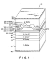
- Fig. 1 of the drawings a transverse mode stabilized double-heterostructure semiconductor laser diode with a mesa strip waveguide structure, which is designated by reference numeral 10.
- Laser diode 10 has an n type GaAs substrate 12 of high impurity concentration.
- n type GaAs buffer layer 14 On one side of substrate 12 are disposed one above another an n type GaAs buffer layer 14, an n type InGaP buffer layer 16, an n type InAlP cladding layer (first cladding layer) 18, an undoped InGaP active layer 20 serving as a light-emitting layer, a cladding layer unit (second cladding layer) 28 formed of three p type semiconductive layers; namely, InAlP layer 22, InGaAlP layer 24 and InAlP layer 26.
- First cladding layer 18, active layer 20 and second cladding layer 28 constitute a double-heterostructure in laser diode 10.
- the p type InGaAlP layer (referred to as "p-INGaP layer” hereinafter) 24 contains aluminum component at lower composition ratio, as compared with the other p-InAlP layers 22 and 26, to thereby serve as an etching stopper in the manufacturing process of laser diode 10, which will be described in detail later.
- the p-InAlP layer 26 is formed on layer 24 to have a mesa stripe-shape defined by two slanted side surfaces 26a and 26b.
- the p-InAlP layer 26 thus provide a linear projection or rib defining a mesa-like waveguide channel section of laser 10.
- Contact layer 32 is formed also in the mesa stripe shape, the width of which is narrower than that of the cladding layer 26.
- Two p-GaAs layers 34-1 and 34-2 for current-blocking are so formed on cladding layer unit 28 as to cover mesa stripe-shaped cladding layer 26, thin contact layer 30 and mesa stripe-shaped contact layer 32. Only the top surface of contact layer 32 is kept uncovered by current-blocking layers 34. Current-blocking layers 34 are thus in direct contact with the channel side surfaces of stripe-shaped cladding layer 26 and contact layer 30 and 32.
- Mesa stripe-shaped contact layer 32 and layers 34-1 and 34-2 may serve to carry out the current-blocking function for laser 10.
- Contact layer 30 is provided to decrease the electric contact resistivity between cladding layer 26 and contact layer 32.
- Contact layer 30 is comprised of a certain semiconductive material having a band gap which is larger than that of the overlying contact layer 32 and yet smaller than that of the underlying cladding layer 26.
- the band gap may be arranged such that it is varied within contact layer 30.
- a thick p-GaAs contact layer 36 is further provided to cover current-blocking layers 34 and the top surface of mesa stripe-shaped contact layer 32. Since contact layer 36 is thick, its top surface is formed flat, so that laser diode 10 has a square cross section as a whole.
- Flat metal layers 38 and 40 are provided on the other surface of substrate 12 and the top surface of the upper contact layer 36 to thereby sandwich the above laser diode structure, as shown in Fig. 1, whereby these metal layers can serve as terminal electrodes therefor.
- second cladding layer 26 and current-blocking layers 34-1 and 34-2 are formed by different semiconductor materials included in the III-V group.
- second cladding layer 26 contains indium (In) as a III-group semiconductor and phosphorus (P) as a V-group semiconductor; while current-blocking layers 34 contain gallium (Ga) as a III-group semiconductor and arsenic (As) as a V-group semiconductor, with their carrier concentration greater than that of second cladding layer 26.
- the carrier concentration of second cladding layer 26 is greater than 7 ⁇ 1017 cm ⁇ 3, and the carrier concentration of current-blocking layers 34 is greater than 1 ⁇ 1018 cm ⁇ 3 In this embodiment, the carrier concentration of the current-blocking layers is set as high as 2 ⁇ 1018 cm ⁇ 3.
- Cladding layer 26 does not contain the same III-group semiconductor and V-group semiconductor as current-blocking layers 34. Accordingly, a Schottky barrier is formed between second cladding layer 26 and current-blocking layers 34.
- cladding layer 26 is set in an indirect transitional region and has a band gap of about 2.3 electron volts (eV), while current-blocking layers 34 have a band gap of about 1.4 eV.
- the energy level difference De (called “energy discontinuous amount” among those skilled in the art) at the valence band between cladding layer 26 and current-blocking layers 34, which has a lower energy than the conduction band, is increased approximately to 0.6 eV or above.
- the energy level difference De becomes greater than 0.6 eV.
- a Shottky barrier with an energy of 0.6 eV or more exists at the boundary between cladding layer 26 and current-blocking layers 34.
- This barrier is high sufficient to seal current carriers within cladding layer 26, which constitutes the mesa stripe-shaped channel, during the operation of semiconductor laser 10.
- the heterostructure junction having such a large band discontinuity for the current blocking purpose, even when crystal mismatch (crystal defect) is present at the boundary between cladding layer 26 and current-blocking layers 34 (particularly, at slanted surface portions 26a and 26b), it is possible to effectively prevent the crystal defect-originated current leak, namely, the leak of holes from cladding layer 26 to current-blocking layers 34 in this embodiment.
- cladding layer 26 and current-blocking layers 34 have opposite conductivities: cladding layer 26 being of a p type and current-blocking layers 34 of an n type as shown in Fig. 1. According to this embodiment, naturally, a typical pn junction is also formed between cladding layer 26 and current-blocking layers 34. That is, the band gap by the typical pn junction also serves to seal the current carriers within the mesa stripe-shaped channel of semiconductor laser 10. This means desirable strengthening of the current-blocking function.
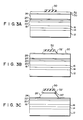
- the MOCVD method under a pressure below the atmospheric pressure was performed using methyl-base III-group organic metals (trimethylindium, trimethylgallium, trimethylaluminum) and V-group hydrides (arsine, phosphine) as raw materials. Using this MOCVD method, as shown in Fig.
- n-GaAs substrate 12 Si dope of 3 ⁇ 1018 cm ⁇ 3 having a face bearing of (100) were sequentially disposed 0.5 ⁇ m thick n-GaAs first buffer layer 14 (Se dope of 3 ⁇ 1018 cm ⁇ 3), 0.5 ⁇ m thick n-InGaP second buffer layer 16 (Se dope of 3 ⁇ 1018 cm ⁇ 3), 1.0 ⁇ m thick n-In 0.5 Al 0.5 P first cladding layer 18 (Se dope of 1 ⁇ 1018 cm ⁇ 3), and 0.1 ⁇ m thick In 0.5 Ga 0.5 P active layer 20.
- second cladding layer 28 On this layer structure were further sequentially disposed three layers constituting second cladding layer 28, namely, 0.1 ⁇ m thick p-In 0.5 Al 0.5 P layer 22 (Mg dope of 1 ⁇ 1018 cm ⁇ 3) 0.01 ⁇ m thick p-In 0.5 Ga 0.5 P layer 24 (Mg dope of 2 ⁇ 1018 cm ⁇ 3) serving as an etching stopper and 1.0 ⁇ m thick p-In 0.5 Al 0.5 P layer 26 (Mg dope of 2 ⁇ 1018 cm ⁇ 3), 0.01 ⁇ m thick p-In 0.5 Ga 0.5 P first contact layer 30 (mg dope of 2 ⁇ 1018 cm ⁇ 3) serving as an intermediate contact layer, and 0.5 ⁇ m thick p-GaAs second contact layer 32 (Mg dope of 2 ⁇ 1018 cm ⁇ 3), thereby forming a double-heterostructure wafer. Then, a 5 ⁇ m wide and 0.1 ⁇ m thick stripe-shaped SiO2 film 50 was formed on
- second contact layer 32 was etched using a GaAs selective etchant to expose first contact layer 30, thus forming a 3 ⁇ m wide GaAs stripe-shaped mesa 32 ⁇ .
- first contact layer 30 was partially etched off using an etchant containing a hydrogen bromide or a hydrogen bromide acid, and first contact layer 30 and cladding layer 26 were etched using an InGaAlP or InAlP selective etchant until cladding layer 24 was exposed, thus forming stripe-shaped mesas (designated by reference numerals "26 ⁇ " and "30 ⁇ ” in Fig. 3C).
- cladding layer 17 serving as the etching stopper may be removed through an etching process using an etchant containing a hydrogen bromide or hydrogen bromide acid.
- second contact layer 32 ⁇ was further etched (or side-etched) to narrower its width, thus forming a narrow stripe-shaped mesa 32 ⁇ shown in Fig. 3D.
- the GaAs selective etchant contained 28% ammonium water, 35% hydrogen peroxide water and water in the ratio of 1:30:9 and was used at the temperature of 20°C.
- the InGaAlP or InAlP selective etchant was sulfuric acid or phosphorous acid and was used at the temperature of 20 to 130°C.
- current-blocking layers 34-1 and 34-2 (Se dope of 5 ⁇ 1018 cm ⁇ 3) were formed to be 0.5 ⁇ m thick using the MOCVD method under a reduced pressure with trimethylgallium and arsine as raw materials.
- the crystal growth was conducted by increasing the temperature up to 830°C while introducing dilute phosphine gas and then cleaning the InAlP surface after waiting about 5 minutes. Thereafter, the phophine gas fluid was switched to the arsine gas fluid and, after waiting about 1 second, the trimethylgallium organic metal was introduced.
- GaAs was not grown at all on SiO2 film 50 and a wafer with the cross section shown in Fig. 3E was attained.
- third contact layer 36 (Mg dope of 5 ⁇ 1018 cm ⁇ 3) with a thickness of 3 ⁇ m was formed on the overall surface of the resultant structure as shown in Fig. 3F, using the MOCVD method. Thereafter, Au/Zu electrode 38 and Au/Ge electrode 40 were respectively formed on the top of third contact layer 36 and the bottom of substrate 12, using a well-known electrode-forming process. As a result, a wafer for a laser that has the structure shown in Fig. 1 was attained.
- this embodiment can provide a highly reliable semiconductor laser with a high reproducibility, which can provide the current-blocking structure and light waveguide structure in self-alignment, and have a single basic transverse mode and a low non-point aberration as well as a stable operation under the feedback of a large amount of external reflection light when InGaAlP that is strongly demanded of a light source for an optical information processing, is used.
- a significantly high barrier (about 0.7 eV) is formed at the valence band between n-GaAs current-blocking layers 34-1 and 34-2 and p-In/alP cladding layer 26 due to the discontinuity of the valence band and the build-in potential at the pn junction.
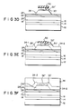
- Fig. 4 is a perspective view of a double-heterostructure semiconductor laser diode according to another embodiment of this invention, which laser diode is designated by reference numeral 60.
- the reference numerals used in Fig. 1 are also used in Fig. 4 to denote corresponding layers for diagrammatic simplicity and ease of understanding, and their explanation will be omitted to avoid redundancy.
- the semiconductor laser diode 60 of Fig. 4 is characterized in its having no current-blocking layers.
- a mesa stripe-shaped second cladding layer 62 is formed on undoped InGaP active layer 20 of laser diode 60.
- This cladding layer 62 comprises a III-V group compound semiconductor, for example, InAlP, whose aluminum composition ratio is increased according to the above-presented inequality (1).
- cladding layer 62 has two slanted side surfaces 62a and 62b.
- p-InGaP contact layer 30 On the narrowed top surface of cladding layer 62 is disposed p-InGaP contact layer 30.
- a p-GaAs contact layer 64 is formed to cover both cladding layer 62 and contact layer 30.
- second cladding layer 62 is in direct contact with p-GaAs contact layer 64.
- This layer structure is equivalent to the one obtained by changing the conductivity of current-blocking layers 34 of semiconductor laser 10 shown in Fig. 1 from n type to p type.
- current-blocking layers 34-1 and 34-2 are GaAs layers that have the opposite conductivity type (n type) to that of second cladding layer 26, while according to the second embodiment of Fig. 4, the current-blocking layers are modified to be formed by GaAs layers that have the same conductivity type (p type) as second cladding layer 62.
- p-GaAs contact layer 64 are integrated with p-GaAs contact layer 64. According to the second embodiment shown in Fig. 4, therefore, it is unnecessary to form a re-grown semiconductor layer constituting an independent current-blocking layer at the current path and a light waveguide section (i.e., the slanted side surfaces of the mesa stripe channel).
- the sealing of current carriers in the mesa stripe-shaped channel while semiconductor layer 60 is emitting a visible laser beam at the ambient temperature is also carried out using the difference in level (non-ohmic contact) of the Shottky barrier that is increased by the discontinuity of the band gap at the boundary section of the channel.
- the conductivity type of the current-blocking layers is changed to p type that is the conductivity type of second cladding layer 62, formation of an independent current-blocking layer can be substantially omitted. Consequently, it is possible to manufacture at a low cost a semiconductor laser (60), which can effectively prevent the current leak in the channel to the degree realized by semiconductor laser 10 of Fig. 1, is highly reliable and has excellent fundamental operation characteristics.
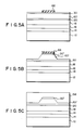
- n-GaAs substrate 12 Si dope of 3 ⁇ 1018 cm ⁇ 3 having a face bearing of (100) were sequentially disposed 0.5 ⁇ m thick n-GaAs first buffer layer 14 (Si dope of 1 ⁇ 1018 cm ⁇ 3) 0.5 ⁇ m thick n-InGaP second buffer layer 16 (Si dope of 1 ⁇ 1018 cm ⁇ 3) 1.0 ⁇ m thick n-In 0.5 Al 0.5 P first cladding layer 18 (Si dope of 1 ⁇ 1018 cm ⁇ 3), 0.07 ⁇ m thick In 0.5 Ga 0.5 P active layer 20, 1.0 ⁇ m thick p-In 0.5 Al 0.5 P second cladding layer 62 (Mg dope of 1 ⁇ 1018 cm ⁇ 3), and 0.1 ⁇ m thick p-In 0.5 Ga 0.5 P intermediate contact layer 30 (Mg dope of 1 ⁇ 1018 cm ⁇ 3), thereby forming a double-
- InGaP intermediate contact layer 30 was etched by a liquid mixture of hydrogen bromide acid, bromine and water, thereby forming stripe-shaped intermediate contact layer 30 ⁇ .
- second cladding layer 62 was half etched by an InGaAlP selective etchant to form a stripe-shaped mesa as shown in Fig. 5B.
- the InGaAlP selective etchant was sulfuric acid or phosphorous acid and was used at the temperature of 15-130°C.
- a Au/Zn electrode and an Au/Ge electrode were formed respectively on the top surface of contact layer 64 and the bottom surface of substrate 12 by a well-known electrode-forming process, thus providing the wafer for a laser that has the structure shown in Fig. 1.
- a semiconductor laser having the current-blocking structure including InGaAlP and the light waveguide structure can easily be prepared without using a special measure, such as a selective layer formation. This semiconductor laser is therefore very effective in this respect.
- the p-type cladding layer comprises InAlP and the n-type current-blocking layer comprises GaAs in the first embodiment
- about the same threshold current was attained when the p-type cladding layer comprises In 1-x-y Ga x Al y P ( x ⁇ 0, y ⁇ 0.35) and the n-type current-blocking layers comprise GaAlAs.
- a low noise reduction characteristic with respect to the external reflection light was attained when the p-type cladding layer comprises In 1-x-y Ga x Al y P ( x ⁇ 0, y ⁇ 0.4).
- the present inventors recently found that since the band discontinuity at the conductive band is small when the p-type cladding layer comprises In 1-x-y Ga x Al y P, the electrons injected into the active layer from the n-type cladding layer leaked into the p-type cladding layer and were recoupled with the holes, thus producing an invalid current that increase the threshold value.
- the cladding layer is in the indirect transitional region so that the recoupling of the electrons and holes is difficult to occur. As a consequence, the invalid current is reduced, thus reducing the threshold value.
- p-type second cladding layer 32 is re-etched after p-type cladding layer 26 is etched to form a stripe-shaped rib.
- this re-etching process should not necessarily be carried out.
- layers 22, 24 and 26 which are p-InGaAlP-based and constitute the second cladding section may be formed by a single layer.
- p-type first contact layer (intermediate contact layer) 30 should not necessarily be used, and third contact layer 36 may be omitted such that electrodes are directly formed on second contact layer 32.
- the bearing of the stripe is parallel to the crystal axis of [011]; however, this invention can also apply to the case where the bearing of the stripe is [0 1].
- the double-heterostructure may be constituted by InGaAlP and the intermediate contact layer may use In 1-x-y Ga x Al y P ( 0 ⁇ y ⁇ 0.4). Further, the contact layer may also use GaAlAs.
- This invention can apply to a laser which uses other materials than have been described with reference to the preferred embodiments, as long as the combination of the materials has a large band discontinuity.
Landscapes
- Physics & Mathematics (AREA)
- Condensed Matter Physics & Semiconductors (AREA)
- General Physics & Mathematics (AREA)
- Electromagnetism (AREA)
- Optics & Photonics (AREA)
- Geometry (AREA)
- Semiconductor Lasers (AREA)
Applications Claiming Priority (4)
| Application Number | Priority Date | Filing Date | Title |
|---|---|---|---|
| JP186505/86 | 1986-08-08 | ||
| JP18650586A JP2555282B2 (ja) | 1986-08-08 | 1986-08-08 | 半導体レ−ザ装置及びその製造方法 |
| JP225842/86 | 1986-09-26 | ||
| JP61225842A JP2659937B2 (ja) | 1986-09-26 | 1986-09-26 | 半導体発光装置 |
Publications (3)
| Publication Number | Publication Date |
|---|---|
| EP0259026A2 true EP0259026A2 (de) | 1988-03-09 |
| EP0259026A3 EP0259026A3 (en) | 1988-10-05 |
| EP0259026B1 EP0259026B1 (de) | 1994-04-27 |
Family
ID=26503811
Family Applications (1)
| Application Number | Title | Priority Date | Filing Date |
|---|---|---|---|
| EP87307041A Expired - Lifetime EP0259026B1 (de) | 1986-08-08 | 1987-08-07 | Doppelheterostruktur-Halbleiterlaser mit streifenförmigem Mesa-Wellenleiter |
Country Status (3)
| Country | Link |
|---|---|
| US (2) | US4809287A (de) |
| EP (1) | EP0259026B1 (de) |
| DE (1) | DE3789695T2 (de) |
Cited By (4)
| Publication number | Priority date | Publication date | Assignee | Title |
|---|---|---|---|---|
| EP0334637A2 (de) * | 1988-03-25 | 1989-09-27 | Kabushiki Kaisha Toshiba | Halbleitervorrichtung |
| EP0384756A2 (de) * | 1989-02-22 | 1990-08-29 | Kabushiki Kaisha Toshiba | Halbleiterlaservorrichtung |
| US5065200A (en) * | 1989-12-21 | 1991-11-12 | Bell Communications Research, Inc. | Geometry dependent doping and electronic devices produced thereby |
| EP0460939A2 (de) * | 1990-06-05 | 1991-12-11 | Matsushita Electric Industrial Co., Ltd. | Halbleiterlaser mit SiGe-Einkristallsubstrat |
Families Citing this family (28)
| Publication number | Priority date | Publication date | Assignee | Title |
|---|---|---|---|---|
| DE68909632T2 (de) * | 1988-02-09 | 1994-03-10 | Toshiba Kawasaki Kk | Halbleiterlaser-Vorrichtung und deren Herstellungsverfahren. |
| US4893313A (en) * | 1988-03-14 | 1990-01-09 | Kabushiki Kaisha Toshiba | Semiconductor laser device which has a double-hetero structure having an optimal layer thickness |
| JP2831667B2 (ja) * | 1988-12-14 | 1998-12-02 | 株式会社東芝 | 半導体レーザ装置及びその製造方法 |
| US5181218A (en) * | 1988-12-14 | 1993-01-19 | Kabushiki Kaisha Toshiba | Manufacturing method of semiconductor laser with non-absorbing mirror structure |
| JP2809691B2 (ja) * | 1989-04-28 | 1998-10-15 | 株式会社東芝 | 半導体レーザ |
| US5153889A (en) * | 1989-05-31 | 1992-10-06 | Kabushiki Kaisha Toshiba | Semiconductor light emitting device |
| US5048035A (en) * | 1989-05-31 | 1991-09-10 | Kabushiki Kaisha Toshiba | Semiconductor light emitting device |
| US5192711A (en) * | 1989-09-18 | 1993-03-09 | Mitsubishi Denki Kabushiki Kaisha | Method for producing a semiconductor laser device |
| US5202895A (en) * | 1990-05-07 | 1993-04-13 | Kabushiki Kaisha Toshiba | Semiconductor device having an active layer made of ingaalp material |
| JP2965668B2 (ja) * | 1990-11-13 | 1999-10-18 | 株式会社東芝 | 半導体レーザ素子及びその製造方法 |
| JP3242967B2 (ja) * | 1992-01-31 | 2001-12-25 | 株式会社東芝 | 半導体発光素子 |
| EP0589727B1 (de) * | 1992-09-25 | 1997-03-19 | The Furukawa Electric Co., Ltd. | Halbleiterlaservorrichtung |
| JPH06296060A (ja) * | 1993-04-08 | 1994-10-21 | Mitsubishi Electric Corp | 半導体可視光レーザダイオードの製造方法 |
| US5523256A (en) * | 1993-07-21 | 1996-06-04 | Matsushita Electric Industrial Co., Ltd. | Method for producing a semiconductor laser |
| US5721751A (en) * | 1993-10-28 | 1998-02-24 | Nippon Telegraph & Telephone Corporation | Semiconductor laser |
| JP2870632B2 (ja) * | 1995-07-13 | 1999-03-17 | 日本電気株式会社 | 半導体光集積回路およびその製造方法 |
| TW336358B (en) | 1997-10-14 | 1998-07-11 | Ind Tech Res Inst | Laser diode for digital versatile disk (DVD) and process for producing the same |
| JP3481458B2 (ja) | 1998-05-14 | 2003-12-22 | アンリツ株式会社 | 半導体レーザ |
| US6613679B2 (en) * | 1999-12-22 | 2003-09-02 | Matsushita Electric Industrial Co., Ltd. | Method for fabricating a semiconductor device |
| JP3726252B2 (ja) * | 2000-02-23 | 2005-12-14 | 独立行政法人理化学研究所 | 紫外発光素子およびInAlGaN発光層の製造方法 |
| JP3763459B2 (ja) * | 2001-06-26 | 2006-04-05 | シャープ株式会社 | 半導体レーザ素子及びその製造方法 |
| JP3866540B2 (ja) | 2001-07-06 | 2007-01-10 | 株式会社東芝 | 窒化物半導体素子およびその製造方法 |
| US8402589B2 (en) | 2001-07-25 | 2013-03-26 | The Libman Company | Cleaning implement |
| US7520018B2 (en) * | 2001-07-25 | 2009-04-21 | The Libman Company | Mop with attached wringer |
| MX2012002552A (es) | 2011-03-04 | 2012-11-30 | Libman Co | Instrumento de limpieza. |
| JP2012252139A (ja) * | 2011-06-02 | 2012-12-20 | Sumitomo Electric Ind Ltd | 半導体光変調器の製造方法及び半導体光変調器 |
| US11158995B2 (en) * | 2018-06-01 | 2021-10-26 | Visual Photonics Epitaxy Co., Ltd. | Laser diode with defect blocking layer |
| US11419472B2 (en) | 2020-03-13 | 2022-08-23 | The Libman Company | Cleaning implement |
Citations (6)
| Publication number | Priority date | Publication date | Assignee | Title |
|---|---|---|---|---|
| US4366568A (en) * | 1979-12-20 | 1982-12-28 | Matsushita Electric Industrial Co. Ltd. | Semiconductor laser |
| EP0114109A2 (de) * | 1983-01-14 | 1984-07-25 | Kabushiki Kaisha Toshiba | Halbleiterlaser-Vorrichtung und Verfahren zu deren Herstellung |
| JPS6045085A (ja) * | 1983-08-22 | 1985-03-11 | Rohm Co Ltd | 半導体レ−ザおよびその製造方法 |
| JPS6174382A (ja) * | 1984-09-20 | 1986-04-16 | Matsushita Electric Ind Co Ltd | 半導体レ−ザ装置およびその製造方法 |
| JPS61125184A (ja) * | 1984-11-22 | 1986-06-12 | Toshiba Corp | 半導体レ−ザ装置 |
| JPS61174685A (ja) * | 1985-01-30 | 1986-08-06 | Hitachi Ltd | 半導体レ−ザ装置及びその作製方法 |
Family Cites Families (1)
| Publication number | Priority date | Publication date | Assignee | Title |
|---|---|---|---|---|
| US4821278A (en) * | 1987-04-02 | 1989-04-11 | Trw Inc. | Inverted channel substrate planar semiconductor laser |
-
1987
- 1987-08-07 EP EP87307041A patent/EP0259026B1/de not_active Expired - Lifetime
- 1987-08-07 DE DE3789695T patent/DE3789695T2/de not_active Expired - Lifetime
- 1987-08-10 US US07/083,189 patent/US4809287A/en not_active Expired - Lifetime
-
1988
- 1988-12-05 US US07/279,816 patent/US4949349A/en not_active Expired - Lifetime
Patent Citations (6)
| Publication number | Priority date | Publication date | Assignee | Title |
|---|---|---|---|---|
| US4366568A (en) * | 1979-12-20 | 1982-12-28 | Matsushita Electric Industrial Co. Ltd. | Semiconductor laser |
| EP0114109A2 (de) * | 1983-01-14 | 1984-07-25 | Kabushiki Kaisha Toshiba | Halbleiterlaser-Vorrichtung und Verfahren zu deren Herstellung |
| JPS6045085A (ja) * | 1983-08-22 | 1985-03-11 | Rohm Co Ltd | 半導体レ−ザおよびその製造方法 |
| JPS6174382A (ja) * | 1984-09-20 | 1986-04-16 | Matsushita Electric Ind Co Ltd | 半導体レ−ザ装置およびその製造方法 |
| JPS61125184A (ja) * | 1984-11-22 | 1986-06-12 | Toshiba Corp | 半導体レ−ザ装置 |
| JPS61174685A (ja) * | 1985-01-30 | 1986-08-06 | Hitachi Ltd | 半導体レ−ザ装置及びその作製方法 |
Non-Patent Citations (5)
| Title |
|---|
| APPLIED PHYSICS LETTERS, vol. 38, no. 11, 1st June 1981, pages 845-847, American Institute of Physics, Woodbury, New York, US; J.C. BOULEY et al.: "A Schottky-barrier-delineated stripe structure for a GaInAsP-InP cw laser" * |
| PATENT ABSTRACTS OF JAPAN, vol. 10, no. 244 (E-430)[2300], 22nd August 1986; & JP-A-61 74 382 (MATSUSHITA ELECTRIC IND. CO., LTD) 16-04-1986 * |
| PATENT ABSTRACTS OF JAPAN, vol. 10, no. 313 (E-448)[2369], 24th October 1986; & JP-A-61 125 184 (TOSHIBA CORP.) 12-06-1986 * |
| PATENT ABSTRACTS OF JAPAN, vol. 10, no. 384 (E-466)[2441], 23rd December 1986; & JP-A-61 174 685 (HITACHI LTD) 06-08-1986 * |
| PATENT ABSTRACTS OF JAPAN, vol. 9, no. 173 (E-329)[1896], 18th July 1985; & JP-A-60 45 085 (ROOMU K.K.) 11-03-1985 * |
Cited By (8)
| Publication number | Priority date | Publication date | Assignee | Title |
|---|---|---|---|---|
| EP0334637A2 (de) * | 1988-03-25 | 1989-09-27 | Kabushiki Kaisha Toshiba | Halbleitervorrichtung |
| EP0334637A3 (de) * | 1988-03-25 | 1991-09-25 | Kabushiki Kaisha Toshiba | Halbleitervorrichtung |
| EP0384756A2 (de) * | 1989-02-22 | 1990-08-29 | Kabushiki Kaisha Toshiba | Halbleiterlaservorrichtung |
| EP0384756A3 (de) * | 1989-02-22 | 1991-06-26 | Kabushiki Kaisha Toshiba | Halbleiterlaservorrichtung |
| US5065200A (en) * | 1989-12-21 | 1991-11-12 | Bell Communications Research, Inc. | Geometry dependent doping and electronic devices produced thereby |
| EP0460939A2 (de) * | 1990-06-05 | 1991-12-11 | Matsushita Electric Industrial Co., Ltd. | Halbleiterlaser mit SiGe-Einkristallsubstrat |
| EP0460939A3 (en) * | 1990-06-05 | 1992-07-29 | Matsushita Electric Industrial Co., Ltd | Semiconductor laser device comprising a sige single crystal substrate |
| US5164950A (en) * | 1990-06-05 | 1992-11-17 | Matsushita Electric Industrial Co., Ltd. | Semiconductor laser device comprising a sige single crystal substrate |
Also Published As
| Publication number | Publication date |
|---|---|
| DE3789695D1 (de) | 1994-06-01 |
| EP0259026B1 (de) | 1994-04-27 |
| EP0259026A3 (en) | 1988-10-05 |
| US4809287A (en) | 1989-02-28 |
| DE3789695T2 (de) | 1994-08-25 |
| US4949349A (en) | 1990-08-14 |
Similar Documents
| Publication | Publication Date | Title |
|---|---|---|
| EP0259026B1 (de) | Doppelheterostruktur-Halbleiterlaser mit streifenförmigem Mesa-Wellenleiter | |
| US4910743A (en) | Semiconductor laser with mesa stripe waveguide structure | |
| US4734385A (en) | Semiconductor laser element suitable for production by a MO-CVD method | |
| US5321712A (en) | Semiconductor light-emitting device having a cladding layer composed of an InGaAlp-based compound | |
| JP2555282B2 (ja) | 半導体レ−ザ装置及びその製造方法 | |
| JP2997573B2 (ja) | 半導体レーザ装置 | |
| JP2647076B2 (ja) | 半導体レーザ装置及びその製造方法 | |
| US5149670A (en) | Method for producing semiconductor light emitting device | |
| EP0353033B1 (de) | Halbleiterlaser mit Stegwellenleiter | |
| JPH11284280A (ja) | 半導体レーザ装置及びその製造方法ならびにiii−v族化合物半導体素子の製造方法 | |
| JPH0815228B2 (ja) | 半導体レ−ザ装置及びその製造方法 | |
| EP0604965B1 (de) | Halbleiterlaser mit Begrenzungsschicht aus AlGaInP | |
| US4783425A (en) | Fabrication process of semiconductor lasers | |
| JPH0697592A (ja) | 半導体レーザ及びその製造方法 | |
| JPH10135567A (ja) | 半導体レーザ素子 | |
| US5278857A (en) | Indium gallium aluminum phosphide silicon doped to prevent zinc disordering | |
| EP0614257B1 (de) | Gewinngeführter Diodenlaser | |
| US7208774B2 (en) | Semiconductor optical device | |
| EP1130722A2 (de) | Halbleiterlaservorrichtung | |
| JP3403915B2 (ja) | 半導体レーザ | |
| JP2555984B2 (ja) | 半導体レーザおよびその製造方法 | |
| JPS6237557B2 (de) | ||
| EP0526220A1 (de) | Lichtemittierende Diode mit kleiner Emissionsfläche | |
| JPH09321388A (ja) | 構造基板の製造方法 | |
| JP3194616B2 (ja) | 半導体レーザ装置 |
Legal Events
| Date | Code | Title | Description |
|---|---|---|---|
| PUAI | Public reference made under article 153(3) epc to a published international application that has entered the european phase |
Free format text: ORIGINAL CODE: 0009012 |
|
| AK | Designated contracting states |
Kind code of ref document: A2 Designated state(s): DE FR GB |
|
| 17P | Request for examination filed |
Effective date: 19880209 |
|
| PUAL | Search report despatched |
Free format text: ORIGINAL CODE: 0009013 |
|
| AK | Designated contracting states |
Kind code of ref document: A3 Designated state(s): DE FR GB |
|
| 17Q | First examination report despatched |
Effective date: 19911219 |
|
| GRAA | (expected) grant |
Free format text: ORIGINAL CODE: 0009210 |
|
| AK | Designated contracting states |
Kind code of ref document: B1 Designated state(s): DE FR GB |
|
| REF | Corresponds to: |
Ref document number: 3789695 Country of ref document: DE Date of ref document: 19940601 |
|
| ET | Fr: translation filed | ||
| PLBE | No opposition filed within time limit |
Free format text: ORIGINAL CODE: 0009261 |
|
| STAA | Information on the status of an ep patent application or granted ep patent |
Free format text: STATUS: NO OPPOSITION FILED WITHIN TIME LIMIT |
|
| 26N | No opposition filed | ||
| PGFP | Annual fee paid to national office [announced via postgrant information from national office to epo] |
Ref country code: GB Payment date: 19970729 Year of fee payment: 11 |
|
| PGFP | Annual fee paid to national office [announced via postgrant information from national office to epo] |
Ref country code: FR Payment date: 19970811 Year of fee payment: 11 |
|
| PG25 | Lapsed in a contracting state [announced via postgrant information from national office to epo] |
Ref country code: GB Free format text: LAPSE BECAUSE OF NON-PAYMENT OF DUE FEES Effective date: 19980807 |
|
| GBPC | Gb: european patent ceased through non-payment of renewal fee |
Effective date: 19980807 |
|
| PG25 | Lapsed in a contracting state [announced via postgrant information from national office to epo] |
Ref country code: FR Free format text: LAPSE BECAUSE OF NON-PAYMENT OF DUE FEES Effective date: 19990430 |
|
| REG | Reference to a national code |
Ref country code: FR Ref legal event code: ST |
|
| PGFP | Annual fee paid to national office [announced via postgrant information from national office to epo] |
Ref country code: DE Payment date: 20060803 Year of fee payment: 20 |