EP0257544B1 - Empfangseinrichtung für Mikrowellensignale - Google Patents
Empfangseinrichtung für Mikrowellensignale Download PDFInfo
- Publication number
- EP0257544B1 EP0257544B1 EP87112028A EP87112028A EP0257544B1 EP 0257544 B1 EP0257544 B1 EP 0257544B1 EP 87112028 A EP87112028 A EP 87112028A EP 87112028 A EP87112028 A EP 87112028A EP 0257544 B1 EP0257544 B1 EP 0257544B1
- Authority
- EP
- European Patent Office
- Prior art keywords
- signal
- receiving device
- decoupling
- antenna
- voltage
- Prior art date
- Legal status (The legal status is an assumption and is not a legal conclusion. Google has not performed a legal analysis and makes no representation as to the accuracy of the status listed.)
- Expired - Lifetime
Links
Images
Classifications
-
- H—ELECTRICITY
- H01—ELECTRIC ELEMENTS
- H01Q—ANTENNAS, i.e. RADIO AERIALS
- H01Q9/00—Electrically-short antennas having dimensions not more than twice the operating wavelength and consisting of conductive active radiating elements
- H01Q9/04—Resonant antennas
- H01Q9/0407—Substantially flat resonant element parallel to ground plane, e.g. patch antenna
-
- H—ELECTRICITY
- H01—ELECTRIC ELEMENTS
- H01Q—ANTENNAS, i.e. RADIO AERIALS
- H01Q1/00—Details of, or arrangements associated with, antennas
- H01Q1/12—Supports; Mounting means
- H01Q1/22—Supports; Mounting means by structural association with other equipment or articles
- H01Q1/24—Supports; Mounting means by structural association with other equipment or articles with receiving set
- H01Q1/248—Supports; Mounting means by structural association with other equipment or articles with receiving set provided with an AC/DC converting device, e.g. rectennas
-
- H—ELECTRICITY
- H01—ELECTRIC ELEMENTS
- H01Q—ANTENNAS, i.e. RADIO AERIALS
- H01Q25/00—Antennas or antenna systems providing at least two radiating patterns
- H01Q25/001—Crossed polarisation dual antennas
Definitions
- Receiving device for microwave signals which has a single antenna which is provided with two separate coupling-out connections, the antenna and the arrangement of the coupling-out connections being adapted such that they receive a vertically polarized signal and a horizontally polarized signal.
- a receiving device of the type described above is known (US-E-29 911).
- the antenna is arranged as a printed conductor track on a printed circuit board.
- a receiving device for microwave signals with a large number of dipoles, filters and Schottky diodes is also known.
- a number of receiving devices are connected to each other by a transmission line that supplies a load with DC voltage on the output side in series or in parallel with other transmission lines (N.T.I.S. Tech Notes, February 1984).
- Microwave signals are often transmitted wirelessly and received with antennas using stripline technology.
- a strip line consists of a conductive base area, a dielectric carrier material (substrate plate) arranged above it and a metallized conductor track located thereon.
- the lines known from high-frequency technology with 50 ⁇ characteristic impedance can also be realized on a ceramic substrate.
- the greater losses of microwave strip lines compared to coaxial or hollow lines, which are largely due to ohmic losses, partly to dielectric losses and, in the case of unshielded circuits, to radiation losses, are largely compensated for by the shorter line sections.
- the behavior of idling strip lines to emit electromagnetic waves can be used to manufacture planar antennas. Most commonly used are microwave stripline resonators of length ⁇ / 2.
- the invention is based on the object of further developing a receiving device of the type described in the introduction in such a way that two signals which are closely adjacent in terms of frequency and have different polarization and greatly different amplitude can be received and processed on a module with a space-saving, simple arrangement which can be integrated.
- an energy signal is vertically polarized and a data signal is horizontally polarized
- a voltage doubler circuit for generating an operating voltage and with the decoupling connection for the horizontally polarized data signal as a detector circuit, a diode a load resistor is connected to form a modulated DC voltage.
- the energy signal is e.g. B. in terms of performance a hundred times larger than the data signal, and a close frequency neighborhood of the two transmitted signals, good decoupling and thus high reception quality.
- the arrangement requires little space so that all system functions can be accommodated on one module (substrate plate). Further advantages are evident from the description below.
- the receiving device according to the invention is illuminated by two signals of almost the same frequency (spacing a few MHz).
- the amplitudes of the two signals are very different (c. 20 dB).
- the polarization planes of the emitted signals are shifted from one another by 90 °.
- An unmodulated strong RF carrier P U of large amplitude is radiated linearly polarized vertically (or horizontally), while an amplitude-modulated information signal P M of low amplitude is radiated horizontally (or vertically) linearly polarized.
- the operating range of the transmitted signals is approximately 6 GHz.
- the receiving device consists of an antenna 1 constructed in stripline technology, which receives both the vertically (horizontally) linearly polarized energy signal P U and the horizontally (vertically) linearly polarized data signal P M.
- the antenna provided for the energy signal P U and the data signal P M is in the form of a strip line on a dielectric substrate (usually aluminum oxide ceramic or polytetrafluoroethylene) applied.
- the high-frequency signals from the antenna must be decoupled and processed.
- the RF signals are derived separately via suitable connections on the stripline antenna 1.
- the receiving energy signal P U is fed to the center connection A of the series connection of two diodes D1 and D2.
- This diode circuit is used for rectification and, in conjunction with capacitors, not shown, for voltage doubling and is intended to enable a high output voltage U B at terminals B and C of the series circuit.
- a rectifier circuit with only one diode is of course also possible.
- An unmodulated DC voltage is thus applied to terminals B and C, which can be used, for example, to supply power to active components.
- the data signal P M received by the antenna 1 and offset by 90 ° lies a few MHz next to the energy signal P U , is weaker by a factor of 100 than the energy signal P U and is amplitude-modulated.
- the received signal is rectified at diode D3 and is available at terminal D as a modulated DC voltage U M.
Landscapes
- Waveguide Aerials (AREA)
- Variable-Direction Aerials And Aerial Arrays (AREA)
- Digital Transmission Methods That Use Modulated Carrier Waves (AREA)
- Input Circuits Of Receivers And Coupling Of Receivers And Audio Equipment (AREA)
- Radar Systems Or Details Thereof (AREA)
Description
- Empfangseinrichtung für Mikrowellensignale, die eine einzige Antenne aufweist, die mit zwei getrennten Auskoppelanschlüssen versehen ist, wobei die Antenne und die Anordnung der Auskoppelanschlüsse derart angepasst sind, dass sie ein vertikal polarisiertes Signal und ein horizontal polarisiertes Signal empfangen.
- Eine Empfangseinrichtung der vorstehend beschriebenen Art ist bekannt (US-E-29 911). Die Antenne ist bei dieser Empfangseinrichtung als gedruckte Leiterbahn auf einer Leiterplatte angeordnet.
- Bekannt ist auch eine Empfangseinrichtung für Mikrowellensignale mit einer grossen Zahl von Dipolen, Filtern und Schottky-Dioden. Eine Anzahl von Empfangseirnichtungen ist durch eine Übertragungsleitung miteinander verbunden, die ausgangsseitig in Reihe oder parallel mit anderen Übertragungsleitungen eine Last mit Gleichspannung versorgt (N.T.I.S. Tech Notes, Februar 1984).
- Mikrowellensignale werden vielfach drahtlos übertragen und mit Antennen in Streifenleitungstechnik empfangen. Eine derartige Streifenleitung besteht aus einer leitenden Grundfläche, einem darüber angeordneten dielektrischen Trägermaterial (Substratplättchen) und einer darauf befindlichen metallisierten Leiterbahn. Durch geeignete Dimensionierung der Streifenleitungen lassen sich auch auf einem Keramiksubstrat die von der Hochfrequenztechnik bekannten Leitungen mit 50 Ω Wellenwiderstand realisieren. Die gegenüber Koaxial- oder Hohlleitungen grösseren Verluste von Mikrowellenstreifenleitungen, die zum grossen Teil auf ohmschen Verlusten, zum kleineren Teil auf dielektrischen Verlusten und bei nicht abgeschirmten Schaltungen auf Abstrahlverlusten beruhen, werden durch die kürzeren Leitungsstrecken weitgehend kompensiert.
- Das Verhalten leerlaufender Streifenleitungen, elektromagnetische Wellen abzustrahlen, lässt sich zur Herstellung planarer Antennen ausnutzen. Am häufigsten dienen dazu Mikrowellenstreifenleitungs-Resonatoren der Länge λ/2.
- Der Erfindung liegt die Aufgabe zugrunde, eine Empfangseinrichtung der eingangs beschriebenen Art dahingehend weiterzuentwickeln, dass zwei frequenzmässig eng benachbarte Signale mit unterschiedlicher Polarisation und stark unterschiedlicher Amplitude mit einer platzsparenden, einfachen Anordnung, die integrierbar ist, auf einem Modul empfangen und weiterverarbeitet werden können.
- Die Aufgabe wird erfindungsgemäss dadurch gelöst, dass ein Energiesignal vertikal polarisiert und ein Datensignal horizontal polarisiert ist und dass mit dem Auskoppelanschluss für das vertikal polarisierte Energiesignal als Detektorschaltung eine Spannungsverdopplerschaltung zur Erzeugung einer Betriebsspannung und mit dem Auskoppelanschluss für das horizontal polarisierte Datensignal als Detektorschaltung eine Diode mit einem Arbeitswiderstand zur Bildung einer modulierten Gleichspannung verbunden ist. Mit dieser Anordnung ergibt sich auch bei hohen Leistungsunterschieden, das Energiesignal ist z. B. von der Leistung her hundertmal grösser als das Datensignal, und einer engen Frequenznachbarschaft der beiden übertragenen Signale eine gute Entkopplung und damit eine hohe Empfangsqualität. Die Anordnung benötigt wenig Raum, so dass alle Systemfunktionen auf einem Modul (Substratplatte) untergebracht werden können. Weitere Vorteile sind aus der nachfolgenden Beschreibung ersichtlich.
- Die Erfindung wird im folgenden anhand eines in einer Zeichnung dargestellten Ausführungsbeispiels näher beschrieben.
- Es zeigen:
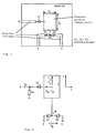
- Fig. 1
- eine in Streifenleitungstechnik ausgeführte Empfangsschaltung und
- Fig. 2
- das zu Fig. 1 gehörende elektrische Schaltbild.
- Die erfindungsgemäße Empfangseinrichtung wird von zwei nahezu gleichfrequenten (Abstand einige MHz) Signalen angestrahlt.
- Die Amplituden der beiden Signale sind dagegen sehr unterschiedlich (c. 20 dB). Die Polarisationsebenen der abgestrahlten Signale sind um 90° gegeneinander verschoben.
- Ein unmodulierter starker HF-Träger PU großer Amplitude wird vertikal (oder horizontal) linear polarisiert abgestrahlt, während ein amplitudenmoduliertes Informationssignal PM geringer Amplitude horizontal (oder vertikal) linear polarisiert abgestrahlt wird. Der Arbeitsbereich der übertragenen Signale liegt bei ungefähr 6 GHz.
- Die Empfangseinrichtung besteht aus einer in Streifenleitungstechnik aufgebauten Antenne 1, die sowohl das vertikal (horizontal) linear polarisierte Energiesignal PU als auch das horizontal (vertikal) linear polarisierte Datensignal PM empfängt. Dabei sind die Abmessungen der Antennenstruktur so gewählt, daß die Länge in x-Richtung der halben Leitungswellenlänge des Signals PU entspricht

während die Länge in y-Richtung (ly) genau
beträgt (c = effektive Ausbreitungsgeschwindigkeit im Substratmaterial). - Die für das Energiesignal PU und das Datensignal PM vorgesehene Antenne ist als Streifenleitung auf ein dielektrisches Substrat (meist Aluminiumoxidkeramik oder Polytetrafluorethylen) aufgetragen. Die hochfrequenzmäßigen Signale von der Antenne müssen ausgekoppelt und weiterverarbeitet werden. Dazu werden über geeignete Anschlüsse auf der Streifenleitungsantenne 1 die HF-Signale getrennt abgeleitet. Das empfangende Energiesignal PU wird dabei auf den Mittelanschluß A der Reihenschaltung von zwei Dioden D1 und D2 geführt. Diese Diodenschaltung dient zur Gleichrichtung und in Verbindung mit nicht dargestellten Kapazitäten zur Spannungsverdopplung und soll eine hohe Ausgangsspannung UB an den Klemmen B und C der Reihenschaltung ermöglichen. Eine Gleichrichterschaltung mit nur einer Diode ist selbstverständlich ebenfalls möglich. An den Klemmen B und C liegt somit eine unmodulierte Gleichspannung, die beispielsweise zur Spannungsversorgung für aktive Bauteile verwendet werden kann.
- Das von der Antenne 1 empfangene, um 90° versetzte Datensignal PM liegt einige MHz neben dem Energiesignal PU, ist um den Faktor 100 schwächer als das Energiesignal PU und ist amplitudenmoduliert. Das empfangene Signal wird an der Diode D3 gleichgerichtet und steht an der Klemme D als modulierte Gleichspannung UM zur Verfügung.
Claims (1)
- Empfangseinrichtung für Mikrowellensignale, die eine einzige Antenne (1) aufweist, die mit zwei getrennten Auskoppelanschlüssen versehen ist, wobei die Antenne und die Anordnung der Auskoppelanschlüsse derart angepasst sind, dass sie ein vertikal polarisiertes Signal und ein horizontal polarisiertes Datensignal empfangen,
dadurch gekennzeichnet,
dass das vertikal polarisierte Signal ein Energiesignal ist und dass mit dem Auskoppelanschluss für das vertikal polarisierte Energiesignal als Detektorschaltung eine Spannungsverdopplerschaltung (D1, D2) zur Erzeugung einer Betriebsspannung und mit dem Auskoppelanschluss für das horizontal polarisierte Datensignal als Detektorschaltung eine Diode (3) mit einem Arbeitswiderstand (R) zur Bildung einer modulierten Gleichspannung (UM) verbunden ist.
Applications Claiming Priority (2)
| Application Number | Priority Date | Filing Date | Title |
|---|---|---|---|
| DE3628583 | 1986-08-22 | ||
| DE3628583A DE3628583C2 (de) | 1986-08-22 | 1986-08-22 | Empfangseinrichtung für Mikrowellensignale |
Publications (3)
| Publication Number | Publication Date |
|---|---|
| EP0257544A2 EP0257544A2 (de) | 1988-03-02 |
| EP0257544A3 EP0257544A3 (en) | 1988-12-07 |
| EP0257544B1 true EP0257544B1 (de) | 1993-06-09 |
Family
ID=6307976
Family Applications (1)
| Application Number | Title | Priority Date | Filing Date |
|---|---|---|---|
| EP87112028A Expired - Lifetime EP0257544B1 (de) | 1986-08-22 | 1987-08-19 | Empfangseinrichtung für Mikrowellensignale |
Country Status (4)
| Country | Link |
|---|---|
| US (1) | US4918749A (de) |
| EP (1) | EP0257544B1 (de) |
| JP (1) | JP2812680B2 (de) |
| DE (2) | DE3628583C2 (de) |
Families Citing this family (28)
| Publication number | Priority date | Publication date | Assignee | Title |
|---|---|---|---|---|
| GB2211357A (en) * | 1987-09-23 | 1989-06-28 | Philips Electronic Associated | Integrated millimetre-wave transceiver |
| US5142698A (en) * | 1988-06-08 | 1992-08-25 | Nec Corporation | Microwave integrated apparatus including antenna pattern for satellite broadcasting receiver |
| GB8816276D0 (en) * | 1988-07-08 | 1988-08-10 | Marconi Co Ltd | Waveguide coupler |
| JPH07104409B2 (ja) * | 1988-08-31 | 1995-11-13 | 山武ハネウエル株式会社 | 無線受信装置 |
| JP2568429B2 (ja) * | 1988-08-31 | 1997-01-08 | 山武ハネウエル株式会社 | 無線応答装置 |
| JP2612190B2 (ja) * | 1988-08-31 | 1997-05-21 | 山武ハネウエル株式会社 | 応答装置と質問装置からなる全二重通信装置 |
| CA1307842C (en) * | 1988-12-28 | 1992-09-22 | Adrian William Alden | Dual polarization microstrip array antenna |
| JPH0636492B2 (ja) * | 1989-04-03 | 1994-05-11 | 山武ハネウエル株式会社 | マイクロ波電力受信装置 |
| JPH0683551B2 (ja) * | 1989-06-02 | 1994-10-19 | 山武ハネウエル株式会社 | 無線受信装置 |
| JPH03120113U (de) * | 1990-03-22 | 1991-12-10 | ||
| US5127102A (en) * | 1991-01-15 | 1992-06-30 | Raytheon Company | Radio frequency mixer circuits |
| US5398035A (en) | 1992-11-30 | 1995-03-14 | The United States Of America As Represented By The Administrator Of The National Aeronautics And Space Administration | Satellite-tracking millimeter-wave reflector antenna system for mobile satellite-tracking |
| US5530637A (en) * | 1993-03-11 | 1996-06-25 | Matsushita Electric Industrial Co., Ltd. | Electric power receiving circuit and responder for automatic vehicle identification system including the same |
| US5394159A (en) * | 1993-11-02 | 1995-02-28 | At&T Corp. | Microstrip patch antenna with embedded detector |
| JP3063513B2 (ja) * | 1994-02-10 | 2000-07-12 | 松下電器産業株式会社 | マイクロ波検波給電回路 |
| US5512911A (en) * | 1994-05-09 | 1996-04-30 | Disys Corporation | Microwave integrated tuned detector |
| US5943016A (en) * | 1995-12-07 | 1999-08-24 | Atlantic Aerospace Electronics, Corp. | Tunable microstrip patch antenna and feed network therefor |
| US5777581A (en) * | 1995-12-07 | 1998-07-07 | Atlantic Aerospace Electronics Corporation | Tunable microstrip patch antennas |
| GB9705870D0 (en) * | 1997-03-21 | 1997-05-07 | Philips Electronics Nv | Charging of secondary cells using transmitted microwave energy |
| JP3413081B2 (ja) * | 1997-10-17 | 2003-06-03 | 株式会社東芝 | 検波回路 |
| DE19851058A1 (de) * | 1998-11-05 | 2000-05-18 | Trw Automotive Electron & Comp | Sende- und/oder Empfangseinrichtung insbesondere für ein Kfz |
| EP1734461A2 (de) | 1999-07-12 | 2006-12-20 | Matsushita Electric Industrial Co., Ltd. | Mobile Körperunterscheidungsvorrichtung zur raschen Erfassung entsprechender von Transpondern innerhalb eines Kommunikationsbereiches eines Interrogatorgeräts über Modulation von reflektierten Funkwellen übertragener Datensätze |
| US7180402B2 (en) * | 2000-06-06 | 2007-02-20 | Battelle Memorial Institute K1-53 | Phase modulation in RF tag |
| US7002517B2 (en) * | 2003-06-20 | 2006-02-21 | Anritsu Company | Fixed-frequency beam-steerable leaky-wave microstrip antenna |
| EP1970994A1 (de) * | 2007-03-12 | 2008-09-17 | Nederlandse Organisatie voor toegepast- natuurwetenschappelijk onderzoek TNO | Eine gleichstromliefernde Antennenanordnung |
| US8144066B2 (en) * | 2009-02-26 | 2012-03-27 | Harris Corporation | Wireless communications including an antenna for wireless power transmission and data communication and associated methods |
| RU2519389C1 (ru) * | 2012-11-12 | 2014-06-10 | Корпорация "САМСУНГ ЭЛЕКТРОНИКС Ко., Лтд." | Малогабаритный резонатор для беспроводной передачи энергии и его интеграции с антенной для передачи данных |
| CN103474778B (zh) * | 2013-09-13 | 2015-09-09 | 电子科技大学 | 一种双频率接收天线及双频率整流天线 |
Family Cites Families (10)
| Publication number | Priority date | Publication date | Assignee | Title |
|---|---|---|---|---|
| US3921177A (en) * | 1973-04-17 | 1975-11-18 | Ball Brothers Res Corp | Microstrip antenna structures and arrays |
| DE2508201C2 (de) * | 1975-02-26 | 1983-02-10 | Brown, Boveri & Cie Ag, 6800 Mannheim | Vorrichtung zur berührungslosen Eingangs- und Ausgangskontrolle von Transportbehältern |
| JPS5456522U (de) * | 1977-09-28 | 1979-04-19 | ||
| JPS5679504A (en) * | 1979-12-03 | 1981-06-30 | Nec Corp | Frequency converter |
| FR2519809A1 (fr) * | 1982-01-08 | 1983-07-18 | Meyer Sylvain | Circuit hyperfrequences multifonction et dispositifs de transmission bidirectionnelle utilisant un tel circuit |
| JPS611102A (ja) * | 1984-01-13 | 1986-01-07 | Japan Radio Co Ltd | 偏波切換えマイクロストリツプアンテナ回路 |
| DE3580922D1 (de) * | 1984-01-19 | 1991-01-24 | Clesse Mandet Sa | Druckminderventil. |
| US4679249A (en) * | 1984-02-15 | 1987-07-07 | Matsushita Electric Industrial Co., Ltd. | Waveguide-to-microstrip line coupling arrangement and a frequency converter having the coupling arrangement |
| CA1238953A (en) * | 1985-02-01 | 1988-07-05 | Nec Corporation | Mixer circuit |
| DE3507865A1 (de) * | 1985-03-06 | 1986-09-11 | Philips Patentverwaltung Gmbh, 2000 Hamburg | Schaltungsanordnung fuer einen tuner zur umschaltung mehrerer frequenzbereiche |
-
1986
- 1986-08-22 DE DE3628583A patent/DE3628583C2/de not_active Expired - Fee Related
-
1987
- 1987-08-19 EP EP87112028A patent/EP0257544B1/de not_active Expired - Lifetime
- 1987-08-19 DE DE8787112028T patent/DE3786124D1/de not_active Expired - Fee Related
- 1987-08-20 JP JP62207372A patent/JP2812680B2/ja not_active Expired - Fee Related
- 1987-08-21 US US07/088,062 patent/US4918749A/en not_active Expired - Lifetime
Also Published As
| Publication number | Publication date |
|---|---|
| DE3628583C2 (de) | 1993-12-09 |
| EP0257544A3 (en) | 1988-12-07 |
| US4918749A (en) | 1990-04-17 |
| DE3628583A1 (de) | 1988-03-10 |
| DE3786124D1 (de) | 1993-07-15 |
| JPS6354023A (ja) | 1988-03-08 |
| EP0257544A2 (de) | 1988-03-02 |
| JP2812680B2 (ja) | 1998-10-22 |
Similar Documents
| Publication | Publication Date | Title |
|---|---|---|
| EP0257544B1 (de) | Empfangseinrichtung für Mikrowellensignale | |
| DE4017625C2 (de) | Mikrowellen-Antwortsender | |
| DE69222464T2 (de) | Mikrostreifenantenne | |
| DE10124142B4 (de) | Planarantenne und damit ausgerüstete Einrichtung für drahtlose Kommunikation | |
| DE69611470T2 (de) | Detektor- und Modulator- Schaltkreise für eine passive Mikrowellenverbindung | |
| DE69528747T2 (de) | Miniatur-Streifenleitungsantenne mit mehreren Zweigen | |
| DE68920631T2 (de) | Rückstrahlantenne. | |
| DE69413988T2 (de) | 3-dimensionales gehäuse für monolithische integrierte mikrowellen/millimeterwelleterwellen-schaltungen | |
| DE69836431T2 (de) | Steuerschaltung für reaktive lasten | |
| DE69931204T2 (de) | Mikrowellen und Millimeterwellen-Vorrichtung | |
| DE69119793T2 (de) | Gehäuse für Hochfrequenzschaltung | |
| DE2633757A1 (de) | Mehrfachantenne | |
| DE2846472A1 (de) | Abschlussvorrichtung einer mikrowellenuebertragungsleitung | |
| DE102004034768B4 (de) | Identifikations-Datenträger | |
| DE69706584T2 (de) | Antenneneinheit | |
| DE60122029T2 (de) | Blitzschutz für eine aktive Antenne mit Patch/Mikrostreifenleiterelementen | |
| DE3202329C2 (de) | ||
| WO1998027440A1 (de) | Transponder mit einer mikrowellen-empfangsantenne | |
| DE10156073A1 (de) | Folienbatterie für tragbare Datenträger mit Antennenfunktion | |
| DE19731085A1 (de) | Einrichtung zum Senden und Empfangen von Radarwellen, insbesondere für einen Abstandssensor | |
| WO1983003309A1 (en) | Doppler radar area monitor | |
| DE60107366T2 (de) | Mischer unter Verwendung einer Diode | |
| DE69320859T2 (de) | Flache, elliptisch polarisierte Antenne | |
| DE2745566C2 (de) | Kopplungsanordnung für eine Mikrostrip-Schaltung mit integriertem Halbleiter-Bauelement | |
| EP0780969B1 (de) | Frequenzmischer für ein Dopplerradarmodul |
Legal Events
| Date | Code | Title | Description |
|---|---|---|---|
| PUAI | Public reference made under article 153(3) epc to a published international application that has entered the european phase |
Free format text: ORIGINAL CODE: 0009012 |
|
| AK | Designated contracting states |
Kind code of ref document: A2 Designated state(s): BE DE FR GB IT |
|
| PUAL | Search report despatched |
Free format text: ORIGINAL CODE: 0009013 |
|
| RAP1 | Party data changed (applicant data changed or rights of an application transferred) |
Owner name: ASEA BROWN BOVERI AKTIENGESELLSCHAFT |
|
| AK | Designated contracting states |
Kind code of ref document: A3 Designated state(s): BE DE FR GB IT |
|
| RAP1 | Party data changed (applicant data changed or rights of an application transferred) |
Owner name: LICENTIA PATENT-VERWALTUNGS-GMBH |
|
| 17P | Request for examination filed |
Effective date: 19890406 |
|
| 17Q | First examination report despatched |
Effective date: 19911218 |
|
| GRAA | (expected) grant |
Free format text: ORIGINAL CODE: 0009210 |
|
| AK | Designated contracting states |
Kind code of ref document: B1 Designated state(s): BE DE FR GB IT |
|
| REF | Corresponds to: |
Ref document number: 3786124 Country of ref document: DE Date of ref document: 19930715 |
|
| ET | Fr: translation filed | ||
| ITF | It: translation for a ep patent filed | ||
| GBT | Gb: translation of ep patent filed (gb section 77(6)(a)/1977) |
Effective date: 19930913 |
|
| PLBE | No opposition filed within time limit |
Free format text: ORIGINAL CODE: 0009261 |
|
| STAA | Information on the status of an ep patent application or granted ep patent |
Free format text: STATUS: NO OPPOSITION FILED WITHIN TIME LIMIT |
|
| 26N | No opposition filed | ||
| ITPR | It: changes in ownership of a european patent |
Owner name: CESSIONE;BAUMER ELECTRIC AG |
|
| REG | Reference to a national code |
Ref country code: GB Ref legal event code: 732E |
|
| REG | Reference to a national code |
Ref country code: FR Ref legal event code: TP |
|
| REG | Reference to a national code |
Ref country code: GB Ref legal event code: 732E |
|
| REG | Reference to a national code |
Ref country code: GB Ref legal event code: IF02 |
|
| PGFP | Annual fee paid to national office [announced via postgrant information from national office to epo] |
Ref country code: GB Payment date: 20020816 Year of fee payment: 16 |
|
| PGFP | Annual fee paid to national office [announced via postgrant information from national office to epo] |
Ref country code: FR Payment date: 20020822 Year of fee payment: 16 |
|
| PGFP | Annual fee paid to national office [announced via postgrant information from national office to epo] |
Ref country code: BE Payment date: 20020829 Year of fee payment: 16 |
|
| PGFP | Annual fee paid to national office [announced via postgrant information from national office to epo] |
Ref country code: DE Payment date: 20020923 Year of fee payment: 16 |
|
| PG25 | Lapsed in a contracting state [announced via postgrant information from national office to epo] |
Ref country code: GB Free format text: LAPSE BECAUSE OF NON-PAYMENT OF DUE FEES Effective date: 20030819 |
|
| PG25 | Lapsed in a contracting state [announced via postgrant information from national office to epo] |
Ref country code: BE Free format text: LAPSE BECAUSE OF NON-PAYMENT OF DUE FEES Effective date: 20030831 |
|
| BERE | Be: lapsed |
Owner name: *BAUMER ELECTRIC A.G. Effective date: 20030831 |
|
| PG25 | Lapsed in a contracting state [announced via postgrant information from national office to epo] |
Ref country code: DE Free format text: LAPSE BECAUSE OF NON-PAYMENT OF DUE FEES Effective date: 20040302 |
|
| GBPC | Gb: european patent ceased through non-payment of renewal fee |
Effective date: 20030819 |
|
| PG25 | Lapsed in a contracting state [announced via postgrant information from national office to epo] |
Ref country code: FR Free format text: LAPSE BECAUSE OF NON-PAYMENT OF DUE FEES Effective date: 20040430 |
|
| REG | Reference to a national code |
Ref country code: FR Ref legal event code: ST |
|
| PG25 | Lapsed in a contracting state [announced via postgrant information from national office to epo] |
Ref country code: IT Free format text: LAPSE BECAUSE OF NON-PAYMENT OF DUE FEES;WARNING: LAPSES OF ITALIAN PATENTS WITH EFFECTIVE DATE BEFORE 2007 MAY HAVE OCCURRED AT ANY TIME BEFORE 2007. THE CORRECT EFFECTIVE DATE MAY BE DIFFERENT FROM THE ONE RECORDED. Effective date: 20050819 |