EP0251578B1 - Quantumquellen-Leitungen und -Büchsen enthaltende Halbleiterstrukturen - Google Patents
Quantumquellen-Leitungen und -Büchsen enthaltende Halbleiterstrukturen Download PDFInfo
- Publication number
- EP0251578B1 EP0251578B1 EP87305397A EP87305397A EP0251578B1 EP 0251578 B1 EP0251578 B1 EP 0251578B1 EP 87305397 A EP87305397 A EP 87305397A EP 87305397 A EP87305397 A EP 87305397A EP 0251578 B1 EP0251578 B1 EP 0251578B1
- Authority
- EP
- European Patent Office
- Prior art keywords
- regions
- quantum well
- recited
- interdiffusion
- bandgap
- Prior art date
- Legal status (The legal status is an assumption and is not a legal conclusion. Google has not performed a legal analysis and makes no representation as to the accuracy of the status listed.)
- Expired - Lifetime
Links
Images

Classifications
-
- H—ELECTRICITY
- H10—SEMICONDUCTOR DEVICES; ELECTRIC SOLID-STATE DEVICES NOT OTHERWISE PROVIDED FOR
- H10P—GENERIC PROCESSES OR APPARATUS FOR THE MANUFACTURE OR TREATMENT OF DEVICES COVERED BY CLASS H10
- H10P14/00—Formation of materials, e.g. in the shape of layers or pillars
- H10P14/20—Formation of materials, e.g. in the shape of layers or pillars of semiconductor materials
- H10P14/38—Formation of materials, e.g. in the shape of layers or pillars of semiconductor materials characterised by treatments done after the formation of the materials
- H10P14/3824—Intermixing, interdiffusion or disordering of III-V heterostructures, e.g. IILD
-
- B—PERFORMING OPERATIONS; TRANSPORTING
- B82—NANOTECHNOLOGY
- B82Y—SPECIFIC USES OR APPLICATIONS OF NANOSTRUCTURES; MEASUREMENT OR ANALYSIS OF NANOSTRUCTURES; MANUFACTURE OR TREATMENT OF NANOSTRUCTURES
- B82Y10/00—Nanotechnology for information processing, storage or transmission, e.g. quantum computing or single electron logic
-
- B—PERFORMING OPERATIONS; TRANSPORTING
- B82—NANOTECHNOLOGY
- B82Y—SPECIFIC USES OR APPLICATIONS OF NANOSTRUCTURES; MEASUREMENT OR ANALYSIS OF NANOSTRUCTURES; MANUFACTURE OR TREATMENT OF NANOSTRUCTURES
- B82Y20/00—Nanooptics, e.g. quantum optics or photonic crystals
-
- H—ELECTRICITY
- H10—SEMICONDUCTOR DEVICES; ELECTRIC SOLID-STATE DEVICES NOT OTHERWISE PROVIDED FOR
- H10D—INORGANIC ELECTRIC SEMICONDUCTOR DEVICES
- H10D62/00—Semiconductor bodies, or regions thereof, of devices having potential barriers
- H10D62/80—Semiconductor bodies, or regions thereof, of devices having potential barriers characterised by the materials
- H10D62/81—Semiconductor bodies, or regions thereof, of devices having potential barriers characterised by the materials of structures exhibiting quantum-confinement effects, e.g. single quantum wells; of structures having periodic or quasi-periodic potential variation
- H10D62/812—Single quantum well structures
- H10D62/813—Quantum wire structures
-
- H—ELECTRICITY
- H10—SEMICONDUCTOR DEVICES; ELECTRIC SOLID-STATE DEVICES NOT OTHERWISE PROVIDED FOR
- H10D—INORGANIC ELECTRIC SEMICONDUCTOR DEVICES
- H10D62/00—Semiconductor bodies, or regions thereof, of devices having potential barriers
- H10D62/80—Semiconductor bodies, or regions thereof, of devices having potential barriers characterised by the materials
- H10D62/81—Semiconductor bodies, or regions thereof, of devices having potential barriers characterised by the materials of structures exhibiting quantum-confinement effects, e.g. single quantum wells; of structures having periodic or quasi-periodic potential variation
- H10D62/812—Single quantum well structures
- H10D62/814—Quantum box structures
-
- H—ELECTRICITY
- H10—SEMICONDUCTOR DEVICES; ELECTRIC SOLID-STATE DEVICES NOT OTHERWISE PROVIDED FOR
- H10D—INORGANIC ELECTRIC SEMICONDUCTOR DEVICES
- H10D62/00—Semiconductor bodies, or regions thereof, of devices having potential barriers
- H10D62/80—Semiconductor bodies, or regions thereof, of devices having potential barriers characterised by the materials
- H10D62/81—Semiconductor bodies, or regions thereof, of devices having potential barriers characterised by the materials of structures exhibiting quantum-confinement effects, e.g. single quantum wells; of structures having periodic or quasi-periodic potential variation
- H10D62/815—Semiconductor bodies, or regions thereof, of devices having potential barriers characterised by the materials of structures exhibiting quantum-confinement effects, e.g. single quantum wells; of structures having periodic or quasi-periodic potential variation of structures having periodic or quasi-periodic potential variation, e.g. superlattices or multiple quantum wells [MQW]
- H10D62/8181—Structures having no potential periodicity in the vertical direction, e.g. lateral superlattices or lateral surface superlattices [LSS]
-
- H—ELECTRICITY
- H10—SEMICONDUCTOR DEVICES; ELECTRIC SOLID-STATE DEVICES NOT OTHERWISE PROVIDED FOR
- H10P—GENERIC PROCESSES OR APPARATUS FOR THE MANUFACTURE OR TREATMENT OF DEVICES COVERED BY CLASS H10
- H10P30/00—Ion implantation into wafers, substrates or parts of devices
- H10P30/20—Ion implantation into wafers, substrates or parts of devices into semiconductor materials, e.g. for doping
- H10P30/22—Ion implantation into wafers, substrates or parts of devices into semiconductor materials, e.g. for doping using masks
-
- H—ELECTRICITY
- H01—ELECTRIC ELEMENTS
- H01S—DEVICES USING THE PROCESS OF LIGHT AMPLIFICATION BY STIMULATED EMISSION OF RADIATION [LASER] TO AMPLIFY OR GENERATE LIGHT; DEVICES USING STIMULATED EMISSION OF ELECTROMAGNETIC RADIATION IN WAVE RANGES OTHER THAN OPTICAL
- H01S5/00—Semiconductor lasers
- H01S5/30—Structure or shape of the active region; Materials used for the active region
- H01S5/34—Structure or shape of the active region; Materials used for the active region comprising quantum well or superlattice structures, e.g. single quantum well [SQW] lasers, multiple quantum well [MQW] lasers or graded index separate confinement heterostructure [GRINSCH] lasers
- H01S5/3413—Structure or shape of the active region; Materials used for the active region comprising quantum well or superlattice structures, e.g. single quantum well [SQW] lasers, multiple quantum well [MQW] lasers or graded index separate confinement heterostructure [GRINSCH] lasers comprising partially disordered wells or barriers
-
- Y—GENERAL TAGGING OF NEW TECHNOLOGICAL DEVELOPMENTS; GENERAL TAGGING OF CROSS-SECTIONAL TECHNOLOGIES SPANNING OVER SEVERAL SECTIONS OF THE IPC; TECHNICAL SUBJECTS COVERED BY FORMER USPC CROSS-REFERENCE ART COLLECTIONS [XRACs] AND DIGESTS
- Y10—TECHNICAL SUBJECTS COVERED BY FORMER USPC
- Y10S—TECHNICAL SUBJECTS COVERED BY FORMER USPC CROSS-REFERENCE ART COLLECTIONS [XRACs] AND DIGESTS
- Y10S438/00—Semiconductor device manufacturing: process
- Y10S438/936—Graded energy gap
-
- Y—GENERAL TAGGING OF NEW TECHNOLOGICAL DEVELOPMENTS; GENERAL TAGGING OF CROSS-SECTIONAL TECHNOLOGIES SPANNING OVER SEVERAL SECTIONS OF THE IPC; TECHNICAL SUBJECTS COVERED BY FORMER USPC CROSS-REFERENCE ART COLLECTIONS [XRACs] AND DIGESTS
- Y10—TECHNICAL SUBJECTS COVERED BY FORMER USPC
- Y10S—TECHNICAL SUBJECTS COVERED BY FORMER USPC CROSS-REFERENCE ART COLLECTIONS [XRACs] AND DIGESTS
- Y10S438/00—Semiconductor device manufacturing: process
- Y10S438/962—Quantum dots and lines
Definitions
- This invention relates generally to semiconductor structures having compositional variations including potential wells for carrier confinement.
- quantum wells Two dimensional quantum well structures were first demonstrated in the GaAs/GaAlAs materials system. In these quantum well structures, the carriers are free to move in two dimensions, but quantum effects are significant in the third dimension. That is, the energy levels are quantized in one dimension but are continuous in the other two dimensions.
- quantum well structures are of interest because, for example, the emission frequency of a double heterostructure laser is shifted from that expected for bulk semiconductors due to the change in allowable energy levels caused by the presence of quantum effects.
- QWW quantum well wires
- QWB quantum well boxes
- Rapid thermal processing which includes rapid thermal annealing, is described in pages 57-58 of S. Wolf and R.N. Taube r Silicon Processing for the VLSI Era.Volume 1: Process Technology , Lattice Press, Sunset Beach, California, USA, 1986.
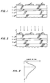
- a structure having an undoped GaAs single quantum well was grown on a (100) GaAs, Cr doped substrate.
- the structure had, sequentially disposed on the substrate 1, a 50 nm GaAs buffer layer, a 50 nm Ga 0.65 Al 0.35 As first barrier layer 3, a 5 nm GaAs quantum well 5, a 50 nm Ga 0.65 Al 0.35 As second barrier layer 7, and a 5 nm GaAs cap layer.
- Masks 9 were formed on the surface from evaporated Ti/Au-Pd films which were approximately 150 nm thick. The films were then patterned using conventional electron beam lithography and lift-off processing. Metal wires and dots having sizes between 50 nm and 1000 nm were fabricated.
- the wires and dots were strips extending into the paper.
- a sectional view of this structure is shown in FIG. 1. For reasons of clarity, only the substrate and the two barrier layers surrounding the quantum well layer are shown as well as the mask.
- Ga+ ions were then implanted into the quantum well region with an energy of 210 keV and a dose which was typically 5 x 1013cm ⁇ 2. This step is schematically depicted in FIG. 2 and the number of ions, as a function of depth z, is depicted in FIG. 3.
- the dose level was typically kept lower than the amorphization threshold. It will be readily appreciated that the implantation step creates a significant number of defects.
- the mask were then removed using a potassium iodide solution for Au-Pd and dilute HF for Ti.
- a rapid thermal anneal was performed at a temperature of approximately 900 degrees C with the epitaxial side of the wafer in contact with the GaAs wafer.
- the rapid thermal anneal of the implanted material results in interdiffusion of Ga and Al across the heterointerface as well as laterally underneath the mask.
- the anneal is typically between 5 and 15 seconds although somewhat longer times, say approximately 5 minutes, can be used.
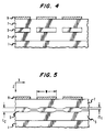
- An idealized representation of the resulting structure is shown in FIG. 4.
- the anneal has resulted in interdiffusion of Ga and Al to form the wires shown. That is, Al and Ga move into and out of, respectively the quantum well region.
- AlGaAs has a larger bandgap than does GaAs, quantum well wires and boxes are formed underneath the mask. As will be understood by those skilled in the art, the wires and boxes are perpendicular to the plane of the page. An anneal for a shorter period will result in less complete interdiffusion of the Ga and Al.
- the particular species chosen for the implant step is not critical. Species other than constituents of the semiconductors may be used. However, the semiconductor must have two species which will interdiffuse. It must also have a compositional profile in which the two species have a varying concentration. The rapid thermal annealing step then permits the two species to come to an equilibrium via the mechanism of the defect enhanced interdiffusion. That is, the diffusion coefficient is much larger in the damaged material than in the undamaged material.
- FIG. 5 A more realistic schematic representation of the resulting structure is depicted in FIG. 5. Depicted are GaAs buffer layer 1, barrier layers 3 and 7, quantum well layer 5, and mask 9.
- L z is the original quantum well layer thickness.
- ⁇ i is the interdiffusion length.
- the variations of the Al concentration along the direction perpendicular, i.e., the z direction, to the interface is given by an error function.
- the local bandgap is proportional to the aluminum concentration.
- GaAs wires are formed under the mask material.
- the energy for implantation is chosen so that the implanted species is deposited in the desired localized region.
- the time and temperature should be sufficiently long and high, respectively, that the desired amount of interdiffusion occurs. It will be appreciated that for some applications complete interdiffusion will not be desired.
- the confinement energy of an electron in a 100 nm quantum well is relatively small, for example, less than 1 meV.
- the potential well profile perpendicular to the wires is characterized by three parameters: (1) the mask size, (2) the implantation lateral straggling, and (3) the diffusion length of the defect which enhances the interdiffusion.
- the confinement effects are either absent or too small to be resolved.
- the profile is not square but rather is rounded. In this potential, the splitting between the first two energy levels is typically larger than in a square well having the same width but it decreases as the quantum number of the energy level increases.
- lateral diffusion i.e., diffusion under the mask.
- diffusion under the mask Some of this is the result of lateral straggling during the implantation step which leads to lateral defect diffusion during the annealing step.
- graded bandgap structures can be easily achieved laterally. This is in contrast to molecular beam epitaxy which typically permits graded bandgap structures to be fabricated only in the vertical, that is, growth, direction.
- a suitable mask is shown in a top view in Fig. 6.
- the implanted zones have a width, w, which increases from left to right. Thus, the implanted area, and thus the dose, also increases. However, the dose per unit area is the same.
- the effective bandgap structure for the thermally annealed AlGaAs is depicted in FIG. 7 for both the conduction and valence bands. As can be seen, the bandgap increases monotonically from left to right as there is more interdiffusion of Al and Ga.
- gratings may be fabricated by using a slight modification, of the mask depicted in Fig. 6. These gratings may be used in many applications, such as, e.g., the external grating in a single frequency laser. Additionally, the grating may be optically coupled to the active layer of a double heterostructure to form a distributed feedback laser. As will be readily appreciated by those skilled in the art, no regrowth over the grating is required. It is also contemplated that the quantum well wires and boxes may be part of semiconductor lasers. Chemical dopants may be added to assist carrier relaxation to the ground state.
Landscapes
- Engineering & Computer Science (AREA)
- Nanotechnology (AREA)
- Chemical & Material Sciences (AREA)
- Crystallography & Structural Chemistry (AREA)
- Physics & Mathematics (AREA)
- Theoretical Computer Science (AREA)
- Mathematical Physics (AREA)
- Life Sciences & Earth Sciences (AREA)
- Biophysics (AREA)
- Optics & Photonics (AREA)
- Semiconductor Lasers (AREA)
- Recrystallisation Techniques (AREA)
- Junction Field-Effect Transistors (AREA)
Claims (5)
- Verfahren zur Herstellung einer Hableiterstruktur mit den Schritten des Implantierens einer Spezis in örtlich festgelegte Bereiche eines kristallinen Halbleiterkörpers, der wenigstens zwei Elemente enthält und in dem wenigstens zwei Heteroübergänge sind, wobei die Implantierung ein Dosisniveau hat, das geringer als die Amorphisierungsschwelle ist, und Erzeugen von Defekten und Erhitzen der kristallinen Halbleiterstruktur,
dadurch gekennzeichnet,
daß das Erhitzen ein schnelles thermisches Wärmebehandlungsverfahren umfaßt, um die Interdiffusion von Atomen von den wenigstens zwei Elementen des Halbleiters über Defekt-unterstützte Mechanismen zu bewirken, wobei die Interdiffusion Bereiche erhöhter Bandlücke erzeugt und dadurch Bereiche, in welchen Ladungsträger mit keinem oder einem Freiheitsgrad eingeschlossen sind, erzeugt. - Verfahren nach Anspruch 1, in welchem die Heteroübergänge einen Potentialtrogbereich bilden, wobei die Spezies in diese Bereiche implantiert ist.
- Verfahren nach Anspruch 2, in welchem die örtlich festgelegten Bereiche einen oder mehrere in zwei Dimensionen eingeschlossene und sich in einer Dimension erstreckende Bereiche definieren.
- Verfahren nach Anspruch 3, in welchem sich die Bereiche in einer Dimension mit sich verändernden Breiten erstrecken.
- Verfahren nach Anspruch 4, in welchem das Wärmebehandeln eine sich lateral ändernde Bandlücke des Halbleiterkörpers erzeugt.
Applications Claiming Priority (2)
| Application Number | Priority Date | Filing Date | Title |
|---|---|---|---|
| US879361 | 1986-06-27 | ||
| US06/879,361 US4751194A (en) | 1986-06-27 | 1986-06-27 | Structures including quantum well wires and boxes |
Publications (3)
| Publication Number | Publication Date |
|---|---|
| EP0251578A2 EP0251578A2 (de) | 1988-01-07 |
| EP0251578A3 EP0251578A3 (en) | 1988-11-09 |
| EP0251578B1 true EP0251578B1 (de) | 1993-12-15 |
Family
ID=25374004
Family Applications (1)
| Application Number | Title | Priority Date | Filing Date |
|---|---|---|---|
| EP87305397A Expired - Lifetime EP0251578B1 (de) | 1986-06-27 | 1987-06-18 | Quantumquellen-Leitungen und -Büchsen enthaltende Halbleiterstrukturen |
Country Status (4)
| Country | Link |
|---|---|
| US (1) | US4751194A (de) |
| EP (1) | EP0251578B1 (de) |
| JP (1) | JPS6310517A (de) |
| DE (1) | DE3788460T2 (de) |
Families Citing this family (27)
| Publication number | Priority date | Publication date | Assignee | Title |
|---|---|---|---|---|
| US4786951A (en) * | 1985-02-12 | 1988-11-22 | Mitsubishi Denki Kabushiki Kaisha | Semiconductor optical element and a process for producing the same |
| US4899201A (en) * | 1987-08-14 | 1990-02-06 | Regents Of The University Of Minnesota | Electronic and optoelectric devices utilizing light hole properties |
| JPH01319985A (ja) * | 1988-06-21 | 1989-12-26 | Matsushita Electric Ind Co Ltd | 化合物半導体量子箱の製造方法およびその製造装置ならびに発光装置 |
| US5229170A (en) * | 1988-06-21 | 1993-07-20 | Matsushita Electric Industrial Co., Ltd. | Method for electrostatically transporting ultrafine particles by use of a needle electrode |
| US5371379A (en) * | 1988-06-21 | 1994-12-06 | Matsushita Electric Industrial Co. Ltd. | Production instrument for producing compound semiconductor quantum boxes and light emitting devices using those quantum boxes |
| JPH0779158B2 (ja) * | 1988-11-19 | 1995-08-23 | 新技術事業団 | 結合量子箱列構造半導体 |
| US4933301A (en) * | 1989-01-27 | 1990-06-12 | Spectra Diode Laboratories, Inc. | Method of forming a semiconductor laser |
| US5436192A (en) * | 1989-03-24 | 1995-07-25 | Xerox Corporation | Method of fabricating semiconductor structures via photo induced evaporation enhancement during in situ epitaxial growth |
| GB8927709D0 (en) * | 1989-12-07 | 1990-02-07 | Secretary Of The State For Def | Silicon quantum wires |
| US5627382A (en) * | 1989-12-07 | 1997-05-06 | The Secretary Of State For Defence In Her Britannic Majesty's Government Of The United Kingdom Of Great Britain And Northern Ireland | Method of making silicon quantum wires |
| FR2656955B1 (fr) * | 1990-01-10 | 1996-12-13 | France Etat | Structure a semiconducteurs pour composant optoelectronique. |
| US5156988A (en) * | 1990-06-30 | 1992-10-20 | Sony Corporation | A method of manufacturing a quantum interference semiconductor device |
| US5225368A (en) * | 1991-02-08 | 1993-07-06 | The United States Of America As Represented By The United States Department Of Energy | Method of producing strained-layer semiconductor devices via subsurface-patterning |
| JP3124305B2 (ja) * | 1991-03-20 | 2001-01-15 | 富士通株式会社 | 光信号波長選択方法および光波長フィルタ |
| US5329137A (en) * | 1991-07-17 | 1994-07-12 | The United States Of America As Represented By The Secretary Of The Air Force | Integrated total internal reflection optical switch utilizing charge storage in a quantum well |
| GB9125727D0 (en) * | 1991-12-03 | 1992-01-29 | Hitachi Europ Ltd | Non-linear optical device |
| US6320200B1 (en) * | 1992-06-01 | 2001-11-20 | Yale University | Sub-nanoscale electronic devices and processes |
| US5475341A (en) * | 1992-06-01 | 1995-12-12 | Yale University | Sub-nanoscale electronic systems and devices |
| JP3182892B2 (ja) * | 1992-07-03 | 2001-07-03 | 松下電器産業株式会社 | 量子素子の製造方法 |
| US5264711A (en) * | 1992-09-15 | 1993-11-23 | The United States Of America As Represented By The Secretary Of The Army | Metal-encapsulated quantum wire for enhanced charge transport |
| JP3500541B2 (ja) * | 1994-02-15 | 2004-02-23 | 富士通株式会社 | 単電子トンネル接合装置の製造方法 |
| GB9503981D0 (en) * | 1995-02-28 | 1995-04-19 | Ca Nat Research Council | Bandag tuning of semiconductor well structures |
| GB0103838D0 (en) * | 2001-02-16 | 2001-04-04 | Univ Glasgow | Improvements in or relating to semiconductor lasers |
| WO2003023817A2 (en) * | 2001-07-20 | 2003-03-20 | The Board Of Trustees Of The University Of Illinois | Process for forming semiconductor quantum dots with superior structural and morphological stability |
| SG99970A1 (en) * | 2002-04-05 | 2003-11-27 | Inst Materials Research & Eng | Method for forming a modified semiconductor having a plurality of band gaps |
| US7405002B2 (en) | 2004-08-04 | 2008-07-29 | Agency For Science, Technology And Research | Coated water-soluble nanoparticles comprising semiconductor core and silica coating |
| US7534489B2 (en) * | 2004-09-24 | 2009-05-19 | Agency For Science, Technology And Research | Coated composites of magnetic material and quantum dots |
Family Cites Families (6)
| Publication number | Priority date | Publication date | Assignee | Title |
|---|---|---|---|---|
| US4194935A (en) * | 1978-04-24 | 1980-03-25 | Bell Telephone Laboratories, Incorporated | Method of making high mobility multilayered heterojunction devices employing modulated doping |
| EP0077825B1 (de) * | 1981-05-06 | 1987-08-12 | University of Illinois Foundation | Verfahren zur herstellung einer zone mit grossem bandabstand innerhalb mehrschichten halbleiter |
| US4503447A (en) * | 1982-07-16 | 1985-03-05 | The United States Of America As Represented By The Secretary Of The Army | Multi-dimensional quantum well device |
| US4581621A (en) * | 1984-07-02 | 1986-04-08 | Texas Instruments Incorporated | Quantum device output switch |
| US4575924A (en) * | 1984-07-02 | 1986-03-18 | Texas Instruments Incorporated | Process for fabricating quantum-well devices utilizing etch and refill techniques |
| US4591889A (en) * | 1984-09-14 | 1986-05-27 | At&T Bell Laboratories | Superlattice geometry and devices |
-
1986
- 1986-06-27 US US06/879,361 patent/US4751194A/en not_active Expired - Lifetime
-
1987
- 1987-06-18 EP EP87305397A patent/EP0251578B1/de not_active Expired - Lifetime
- 1987-06-18 DE DE87305397T patent/DE3788460T2/de not_active Expired - Fee Related
- 1987-06-26 JP JP62159507A patent/JPS6310517A/ja active Pending
Also Published As
| Publication number | Publication date |
|---|---|
| DE3788460D1 (de) | 1994-01-27 |
| JPS6310517A (ja) | 1988-01-18 |
| EP0251578A2 (de) | 1988-01-07 |
| EP0251578A3 (en) | 1988-11-09 |
| US4751194A (en) | 1988-06-14 |
| DE3788460T2 (de) | 1994-04-14 |
Similar Documents
| Publication | Publication Date | Title |
|---|---|---|
| EP0251578B1 (de) | Quantumquellen-Leitungen und -Büchsen enthaltende Halbleiterstrukturen | |
| CA2066002C (en) | Fabrication of quantum devices in compound semiconductor layers and resulting structures | |
| US4771010A (en) | Energy beam induced layer disordering (EBILD) | |
| US4639275A (en) | Forming disordered layer by controlled diffusion in heterojunction III-V semiconductor | |
| EP0232431B1 (de) | Halbleitervorrichtung | |
| EP0660380A2 (de) | Abstimmen des Bandabstands einer halbleitenden Quantumwell-Struktur | |
| JP2686764B2 (ja) | 光半導体素子の製造方法 | |
| US5479027A (en) | Semiconductor device having a channel for a zero-or one-dimensional carrier gas | |
| US4673959A (en) | Heterojunction FET with doubly-doped channel | |
| US4990466A (en) | Method for fabricating index-guided semiconductor laser | |
| US5107306A (en) | Semiconductor device having a waveguide structure | |
| JPS63155713A (ja) | 半導体微細構造の製造法 | |
| DE69029687T2 (de) | Dotierungsverfahren für Halbleiterbauelemente | |
| US5194400A (en) | Method for fabricating a semiconductor laser device using (Alx Ga1-x)y In1-y P semiconductor clad layers | |
| JPH07105490B2 (ja) | 半導体装置 | |
| JP2757258B2 (ja) | 超格子素子の製造方法 | |
| US5346856A (en) | Method of making a selective compositional disordering of a GaAs based heterostructure by the in-diffusion of Au through a single crystal, epitaxially grown Ge film | |
| JP2762800B2 (ja) | 量子細線構造の製造方法 | |
| EP0437702B1 (de) | Integrierte Halbleiterschaltung mit Isolationszonen zwischen Komponenten aus Verbindungshalbleitern und Methode zu deren Herstellung | |
| JP3211227B2 (ja) | GaAs層の表面安定化方法、GaAs半導体装置の製造方法および半導体層の形成方法 | |
| JP2803555B2 (ja) | 極微細トンネル障壁の作製方法 | |
| JP2691572B2 (ja) | 化合物半導体装置の製造方法 | |
| JPS62209865A (ja) | 半導体装置の製造方法 | |
| Leier et al. | Fabrication and optical properties of GaAs-quantum wires produced by ion-implantation induced disordering | |
| KR950007484B1 (ko) | 플루오르화물 박막을 이용한 반도체내 불순물 확산방법 |
Legal Events
| Date | Code | Title | Description |
|---|---|---|---|
| PUAI | Public reference made under article 153(3) epc to a published international application that has entered the european phase |
Free format text: ORIGINAL CODE: 0009012 |
|
| AK | Designated contracting states |
Kind code of ref document: A2 Designated state(s): DE FR GB IT |
|
| PUAL | Search report despatched |
Free format text: ORIGINAL CODE: 0009013 |
|
| AK | Designated contracting states |
Kind code of ref document: A3 Designated state(s): DE FR GB IT |
|
| 17P | Request for examination filed |
Effective date: 19890428 |
|
| 17Q | First examination report despatched |
Effective date: 19910411 |
|
| GRAA | (expected) grant |
Free format text: ORIGINAL CODE: 0009210 |
|
| AK | Designated contracting states |
Kind code of ref document: B1 Designated state(s): DE FR GB IT |
|
| REF | Corresponds to: |
Ref document number: 3788460 Country of ref document: DE Date of ref document: 19940127 |
|
| ET | Fr: translation filed | ||
| ITF | It: translation for a ep patent filed | ||
| RAP4 | Party data changed (patent owner data changed or rights of a patent transferred) |
Owner name: AT&T CORP. |
|
| PLBE | No opposition filed within time limit |
Free format text: ORIGINAL CODE: 0009261 |
|
| STAA | Information on the status of an ep patent application or granted ep patent |
Free format text: STATUS: NO OPPOSITION FILED WITHIN TIME LIMIT |
|
| 26N | No opposition filed | ||
| PGFP | Annual fee paid to national office [announced via postgrant information from national office to epo] |
Ref country code: GB Payment date: 20010525 Year of fee payment: 15 Ref country code: FR Payment date: 20010525 Year of fee payment: 15 |
|
| PGFP | Annual fee paid to national office [announced via postgrant information from national office to epo] |
Ref country code: DE Payment date: 20010629 Year of fee payment: 15 |
|
| REG | Reference to a national code |
Ref country code: GB Ref legal event code: IF02 |
|
| PG25 | Lapsed in a contracting state [announced via postgrant information from national office to epo] |
Ref country code: GB Free format text: LAPSE BECAUSE OF NON-PAYMENT OF DUE FEES Effective date: 20020618 |
|
| PG25 | Lapsed in a contracting state [announced via postgrant information from national office to epo] |
Ref country code: DE Free format text: LAPSE BECAUSE OF NON-PAYMENT OF DUE FEES Effective date: 20030101 |
|
| GBPC | Gb: european patent ceased through non-payment of renewal fee |
Effective date: 20020618 |
|
| PG25 | Lapsed in a contracting state [announced via postgrant information from national office to epo] |
Ref country code: FR Free format text: LAPSE BECAUSE OF NON-PAYMENT OF DUE FEES Effective date: 20030228 |
|
| REG | Reference to a national code |
Ref country code: FR Ref legal event code: ST |
|
| PG25 | Lapsed in a contracting state [announced via postgrant information from national office to epo] |
Ref country code: IT Free format text: LAPSE BECAUSE OF NON-PAYMENT OF DUE FEES;WARNING: LAPSES OF ITALIAN PATENTS WITH EFFECTIVE DATE BEFORE 2007 MAY HAVE OCCURRED AT ANY TIME BEFORE 2007. THE CORRECT EFFECTIVE DATE MAY BE DIFFERENT FROM THE ONE RECORDED. Effective date: 20050618 |