EP0249725B1 - Hochspannungshalbleiterschütz - Google Patents
Hochspannungshalbleiterschütz Download PDFInfo
- Publication number
- EP0249725B1 EP0249725B1 EP87106345A EP87106345A EP0249725B1 EP 0249725 B1 EP0249725 B1 EP 0249725B1 EP 87106345 A EP87106345 A EP 87106345A EP 87106345 A EP87106345 A EP 87106345A EP 0249725 B1 EP0249725 B1 EP 0249725B1
- Authority
- EP
- European Patent Office
- Prior art keywords
- contactor
- ignition
- semiconductor
- voltage
- control section
- Prior art date
- Legal status (The legal status is an assumption and is not a legal conclusion. Google has not performed a legal analysis and makes no representation as to the accuracy of the status listed.)
- Expired - Lifetime
Links
- 239000004065 semiconductor Substances 0.000 claims abstract description 9
- 230000003068 static effect Effects 0.000 claims abstract description 3
- 238000010791 quenching Methods 0.000 claims abstract 6
- 230000000171 quenching effect Effects 0.000 claims abstract 6
- 230000015572 biosynthetic process Effects 0.000 claims description 3
- 229910044991 metal oxide Inorganic materials 0.000 claims description 2
- 150000004706 metal oxides Chemical class 0.000 claims description 2
- 238000001816 cooling Methods 0.000 claims 3
- 230000005540 biological transmission Effects 0.000 claims 2
- 238000000926 separation method Methods 0.000 claims 1
- 238000010276 construction Methods 0.000 abstract description 2
- 238000002955 isolation Methods 0.000 abstract 1
- 230000003321 amplification Effects 0.000 description 1
- 239000003990 capacitor Substances 0.000 description 1
- 125000004122 cyclic group Chemical group 0.000 description 1
- 238000010438 heat treatment Methods 0.000 description 1
- 230000006698 induction Effects 0.000 description 1
- 238000003199 nucleic acid amplification method Methods 0.000 description 1
- XLYOFNOQVPJJNP-UHFFFAOYSA-N water Substances O XLYOFNOQVPJJNP-UHFFFAOYSA-N 0.000 description 1
Images
Classifications
-
- H—ELECTRICITY
- H03—ELECTRONIC CIRCUITRY
- H03K—PULSE TECHNIQUE
- H03K17/00—Electronic switching or gating, i.e. not by contact-making and –breaking
- H03K17/51—Electronic switching or gating, i.e. not by contact-making and –breaking characterised by the components used
- H03K17/56—Electronic switching or gating, i.e. not by contact-making and –breaking characterised by the components used by the use, as active elements, of semiconductor devices
- H03K17/72—Electronic switching or gating, i.e. not by contact-making and –breaking characterised by the components used by the use, as active elements, of semiconductor devices having more than two PN junctions; having more than three electrodes; having more than one electrode connected to the same conductivity region
- H03K17/73—Electronic switching or gating, i.e. not by contact-making and –breaking characterised by the components used by the use, as active elements, of semiconductor devices having more than two PN junctions; having more than three electrodes; having more than one electrode connected to the same conductivity region for DC voltages or currents
- H03K17/732—Measures for enabling turn-off
Definitions
- the invention relates to a high-voltage semiconductor contactor as defined in the preamble of claim 1.
- a power section from the series connection of two GTO thyristors with RCD wiring should be used, as is generally and not specifically related to high-voltage semiconductor contactors, e.g. the Electrotechnical Journal (ETZ), Volume 104, No. 24, December 1983, p. 1246 for GTO thyristors or the Patent Abstracts of Japan for JP-A-52-120669, published October 11, 1977, for normal thyristors.
- the ETZ also deals with overvoltage protection and the abstraction of voltage distribution, both of which are known in the art.
- Semiconductor contactors have properties that can no longer be met by the electromechanical switching devices previously used. The limits of the technical possibilities have been reached there. The switching frequency and service life are high, but limited. Another disadvantage is the wear of the switching elements and bearings, which makes the devices very maintenance-intensive. From this point of view, there are limits and problems for electromechanical high-voltage contactors for applications with a very high switching frequency - in particular cyclic operation.
- the object of the invention is to make it possible to use such a circuit - as initially assumed to be known - for the creation and mechanical implementation of a high-voltage contactor based on semiconductors, which allows wear-free and maintenance-free switching of electrical direct current loads with a very high switching frequency. It is intended for voltages around 1000 V with currents between 0.5 to 15 A and above. It should be simple and compact in its construction and handling, and be able to replace mechanical contactors interchangeably
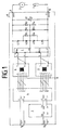
- FIG. 1 shows V3 and V4, two GTO thyristors connected in series, which are combined in a so-called power block 1 and via which a load 3 fed by a DC high-voltage source 2 is switched.
- the anode side is designated with A, the cathode side with K and the cathode / anode-side connection with AK.
- An RCD circuit with elements C1, R5, V2 or C2, R6, V1 is provided for the uniform dynamic reverse voltage distribution of the GTO thyristors V3, V4.
- the static voltage distribution is provided by two times two resistors R1 to R4 connected in parallel.
- Two parallel resistors are on the anode side (A) of the GTO thyristor V4 and two further parallel resistors are on the cathode side (B) of the GTO thistor V3 and they are connected at the voltage divider point to the connection AK of the GTO thyristors.
- a metal oxide varistor R7 is used to protect against line-side overvoltages.
- the ignition and erase pulses for the turn-off thyristors V3, V4 are formed and amplified on a circuit board or printed circuit board 4. The pulses are connected to the GTO thyristors in a valve-isolated manner via special circuit boards 5 and 6, on which ignition transformers are housed.
- the circuit board 7 still shown is used to adapt to the voltage required by the circuit boards 5 and 6 of, for example, DC 60 V. In the assumed case, a supply voltage U S of DC 110 V is available here on the vehicle side. This circuit board 7 can of course be omitted if the Printed circuit boards 5 and 6 can be adapted to the necessary supply voltages via the transformer itself.
- the power section with the power block 1 and the control section with the elements 4 to 7 are accommodated on a ribbed heat sink 8, which also serves as a mounting plate.
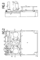
- the mechanical arrangement is shown in Figures 2 and 3.
- the GTO thyristors V3 and V4 of the power block 1 are visible approximately in the middle of the heat sink 8.
- the capacitors C1 and C2 of the RCD circuit are arranged.
- the terminals I, II of the main current path and the flat plugs 9 of the supply voltage U S and the control voltage U C can also be seen in the upper region.
- Fig. 3 additionally shows the position of the parts in a partial side section.
- the solid-state contactor has no contact interruption in the main circuit in the off state. Therefore, when the mains voltage is applied, the main circuit on the load side - even when the contactor is off - must always be regarded as live.
Landscapes
- Emergency Protection Circuit Devices (AREA)
- Bipolar Transistors (AREA)
- Power Conversion In General (AREA)
- Rectifiers (AREA)
- Details Of Television Scanning (AREA)
- Nitrogen Condensed Heterocyclic Rings (AREA)
- Protection Of Static Devices (AREA)
- Electronic Switches (AREA)
- Electric Propulsion And Braking For Vehicles (AREA)
Description
- Die Erfindung bezieht sich auf ein Hochspannungshalbleiterschütz, wie es im Oberbegriff des Anspruches 1 näher definiert ist. Dabei soll ein Leistungsteil aus der Reihenschaltung von zwei GTO-Thyristoren mit RCD-Beschaltung Verwendung finden, wie es generell und nicht speziell auf Hochspannungshalbleiterschütze bezogen z.B. der Elektrotechnischen Zeitschrift (ETZ), Band 104, Nr. 24, Dezember 1983, S. 1246 für GTO-Thyristoren oder den Patent Abstracts of Japan zu JP-A-52-120669, veröffentlicht 11.10.1977, für Normalthyristoren entnehmbar ist. In der ETZ wird auch der Überspannungsschutz und in den Abstracts die Spannungsaufteilung behandelt, beides bekannter Stand der Technik.
- Halbleiterschütze weisen Eigenschaften auf, die von den bisher verwendeten elektromechanischen Schaltgeräten nicht mehr erfüllt werden können. Man ist dort an die Grenzen der technischen Möglichkeiten herangekommen. So ist die Schalthäufigkeit und Lebensdauer zwar schon hoch, jedoch begrenzt. Nachteilig ist auch der Verschleiß der Schaltstücke und Lager, was die Geräte sehr wartungsintensiv macht. Für Anwendungsfälle mit sehr hoher Schalthäufigkeit - insbesondere Taktbetrieb - ergeben sich für elektromechanische Hochspannungsschütze aus dieser Sicht Grenzen und Probleme.
- Aufgabe der Erfindung ist es, eine solche Schaltung - wie sie eingangs als bekannt vorausgesetzt wurde - für die Schaffung und mechanische Realisierung eines Hochspannungsschützes auf Halbleiterbasis nutzbar zu machen, das problemlos ein verschleiß-und wartungsfreies Schalten elektrischer Gleichstromlasten mit sehr hoher Schalthäufigkeit gestattet. Dabei ist an Spannungen um 1000 V mit Strömen zwischen 0,5 bis 15 A und darüber gedacht. Es soll einfach und kompakt im Aufbau und in seiner Montagehandhabung sein und mechanische Schütze austauschbar ersetzen können
- Gelöst-wird diese Aufgabe gemäß den kennzeichnenden Merkmalen des Anspruches 1. Eine vorteilhafte Ausgestaltung ist dem Unteranspruch entnehmbar.
- Es ist zwar schon für HF-Umrichtereinheiten für Induktionshiezung bekannt. Stapel aus abwechselnd geschichteten Normalthyristoren und Wasserkühlern zu bilden (BROWN BOVERIE REVIEW, Band 71, Nr. 5, Mai 1984, S. 219/220, Baden, CH). Das hat jedoch nichts mit der aufgezeigten Erfindung bei Halbleiterschützen zu tun und gibt auch keine Anregung zur Lösung der aufgezeigten Problemstellungen.
- Anhand eines Ausführungsbeispieles wird die Erfindung im nachstehenden näher erläutert.
Es zeigen: - Fig. 1 eine Schaltungsanordung
- Fig. 2 den mechanischen Aufbau eines solchen Schützes
- Fig. 3 einen Seitenschnitt.
- In Fig. 1 sind mit V3 und V4 zwei in Reihe geschaltete GTO-Thyristoren dargestellt, die in einem sogenannten Powerblock 1 zusammengefaßt sind und über die eine von einer Gleich-Hochspannungsquelle 2 gespeiste Last 3 geschaltet wird. Die Anodenseite ist mit A, die Kathodenseite mit K und der kathoden/anodenseitige Zusammenschluß mit AK bezeichnet. Für die gleichmäßige dynamische Sperrspannungsaufteilung der GTO-Thyristoren V3, V4 ist eine RCD-Beschaltung mit den Elementen C1, R5, V2 bzw. C2, R6, V1 vorgesehen. Die statische Spannungsaufteilung wird durch zwei mal zwei parallel geschaltete Widerstände R1 bis R4 besorgt. Je zwei parallele Widerstände liegen anodenseitig (A) am GTO-Thyristor V4 und zwei weitere parallele Widerstände liegen kathodenseitig (B) am GTO-Thristor V3 und sie sind im Spannungsteilerpunkt mit dem Zusammenschluß AK der GTO-Thyristoren verbunden. Zum Schutz vor netzseitigen Überspannungen dient ein Metalloxyde-Varistor R7. Die Zünd- und Löschimpulse für die Abschaltthyristoren V3, V4 werden auf einer Platine oder Leiterplatte 4 gebildet und verstärket. Die Impulse werden ventilgeordnet über spezielle Leiterplatten 5 und 6, auf denen Zündübertrager untergebracht sind, potentialgetrennt an die GTO-Thyristoren geführt. Die noch abgebildete Leiterplatte 7 dient der Anpassung auf die von den Leiterplatten 5 und 6 benötigte Spannung von z.B. DC 60 V. Im angenommenen Fall steht hier fahrzeugseitig eine Versorgungsspannung US von DC 110 V zur Verfügung. Diese Leiterplatte 7 kann natürlich entfallen, wenn die Leiterplatten 5 und 6 über die Übertrager selbst an die nötigen Versorgungsspannungen angepaßt werden. Der Leistungsteil mit dem Powerblock 1 und der Steuerteil mit den Elementen 4 bis 7 sind auf einem verrippten Kühlkörper 8 untergebracht, der gleichzeitig als Montageplatte dient.
- Die mechanische Anordnung geht aus den Figuren 2 und 3 hervor. Etwa in der Mitte vom Kühlkörper 8 sind die GTO-Thyristoren V3 und V4 des Powerblocks 1 sichtbar. Rechts und links daneben (in dieser Ansicht) sind die Kondensatoren C1 und C2 der RCD-Beschaltung angeordnet. Im oberen Bereich sind ferner die Anschlußklemmen I, II des Hauptstrompfades, sowie die Flachstecker 9 der Versorgungsspannung US und der Steuerspannung UCerkennbar.
- Auf dem - hier in dieser Fig.2 - unteren Teil des Kühlkörpers 8 sind in isolierter Doppeletagenanordnung einerseits die zwei Leiterplatten 5 und 6 mit den Zündübertragern für die GTO-Thyristoransteuerung (nur andeutungsweise sichtbar und weitgehend verdeckt) und darüber die weitgehend alles verdeckende Leiterplatte 4 für die Zünd- und Löschimpulsbildung sowie Verstärkung montiert. Eine Leiterplatte 7 zur Anpassung der Versorgungsspannung ist hier nicht vorgesehen.
- Fig. 3 zeigt noch ergänzend die Lage der Teile in einem teilweisen Seitenschnitt.
- Zu beachten ist, daß das Halbleiterschütz im Aus-Zustand keine Kontaktunterbrechung im Hauptstromkreis hat. Daher muß beim Anliegen der Netzspannung der Hauptstromkreis auf der Lastseite - auch im Aus-Zustand des Schützes - immer als spannungsführend angesehen werden.
Claims (2)
- Hochspannungshalbleiterschütz, bei dem der Leistungsteil aus der Reihenschaltung von zwei GTO-Thyristoren (V3,V4) RCD-Beschaltung besteht, denen Mittel zur statischen Spannungsaufteilungund (R1/R3,R2/R4) zum Überspannungsschutz (R7) zugeordnet sein können,
dadurch gekennzeichnet ,
daß der Leistungsteil zusammen mit einem Steuerteil nebeneinander unter Potentialtrennung auf einem gemeinsamen Kühlkörper (8) untergebracht ist, der gleichzeitig als Montageplatte dient und daß dabei der Steuerteil aus einer Platine (4) für die Zünd- und Löschimpulsbildung und zwei weiteren Platinen (5, 6) für die Zünd- und Löschimpulsübertragung gebildet wird, von denen die Platinen (5, 6) für die Zünd- und Löschimpulsübertragung nebeneinander liegend dicht am Kühlkörper angeordnet sind und die Platine (4) für die Zünd- und Löschimpulsbildung etagenartig darüber liegt. - Hochspannungshalbleiterschütz nach Anspruch 1,
dadurch gekennzeichnet,
daß auf dem Kühlkörper (8) noch ein den Ausgangshauptanschlüssen (I, II) des Leistungsteils parallelgeschalteter Überspannungsschutz (R7), vorzugsweise ein Metalloxyd-Varistor, untergebracht ist.
Priority Applications (1)
| Application Number | Priority Date | Filing Date | Title |
|---|---|---|---|
| AT87106345T ATE62092T1 (de) | 1986-06-14 | 1987-05-02 | Hochspannungshalbleiterschuetz. |
Applications Claiming Priority (2)
| Application Number | Priority Date | Filing Date | Title |
|---|---|---|---|
| DE19863620074 DE3620074A1 (de) | 1986-06-14 | 1986-06-14 | Hochspannungshalbleiterschuetz |
| DE3620074 | 1986-06-14 |
Publications (2)
| Publication Number | Publication Date |
|---|---|
| EP0249725A1 EP0249725A1 (de) | 1987-12-23 |
| EP0249725B1 true EP0249725B1 (de) | 1991-03-27 |
Family
ID=6303019
Family Applications (1)
| Application Number | Title | Priority Date | Filing Date |
|---|---|---|---|
| EP87106345A Expired - Lifetime EP0249725B1 (de) | 1986-06-14 | 1987-05-02 | Hochspannungshalbleiterschütz |
Country Status (5)
| Country | Link |
|---|---|
| EP (1) | EP0249725B1 (de) |
| AT (1) | ATE62092T1 (de) |
| DE (2) | DE3620074A1 (de) |
| DK (1) | DK169649B1 (de) |
| ES (1) | ES2021630B3 (de) |
Families Citing this family (4)
| Publication number | Priority date | Publication date | Assignee | Title |
|---|---|---|---|---|
| DE4005333A1 (de) * | 1990-02-20 | 1991-08-22 | Rehm Schweisstechnik Gmbh | Elektronischer leistungs-schalter |
| DE9107692U1 (de) * | 1991-06-21 | 1991-08-14 | Siemens AG, 80333 München | Stromrichterbaueinheit |
| DE10348717B4 (de) * | 2003-10-16 | 2006-09-21 | Hauni Primary Gmbh | Behälter für Tabakmaterial |
| CN103802763B (zh) * | 2014-02-20 | 2015-12-30 | 中国北方车辆研究所 | 一种装甲车辆直流高压大电流组合配电保护装置 |
Family Cites Families (2)
| Publication number | Priority date | Publication date | Assignee | Title |
|---|---|---|---|---|
| US3461319A (en) * | 1967-02-24 | 1969-08-12 | Westinghouse Electric Corp | Secondary slave control for seriesconnected gate controlled switches |
| DE3419652A1 (de) * | 1984-05-25 | 1985-11-28 | Siemens AG, 1000 Berlin und 8000 München | Schaltungsanordnung zum schutz von transienten netzstoerungen von elektronischen stromversorgungseinrichtungen |
-
1986
- 1986-06-14 DE DE19863620074 patent/DE3620074A1/de active Granted
-
1987
- 1987-05-02 EP EP87106345A patent/EP0249725B1/de not_active Expired - Lifetime
- 1987-05-02 AT AT87106345T patent/ATE62092T1/de active
- 1987-05-02 DE DE8787106345T patent/DE3768863D1/de not_active Expired - Fee Related
- 1987-05-02 ES ES87106345T patent/ES2021630B3/es not_active Expired - Lifetime
- 1987-05-20 DK DK256887A patent/DK169649B1/da not_active IP Right Cessation
Also Published As
| Publication number | Publication date |
|---|---|
| ES2021630B3 (es) | 1991-11-16 |
| ATE62092T1 (de) | 1991-04-15 |
| DK256887D0 (da) | 1987-05-20 |
| DE3620074C2 (de) | 1989-03-23 |
| EP0249725A1 (de) | 1987-12-23 |
| DE3768863D1 (de) | 1991-05-02 |
| DE3620074A1 (de) | 1987-12-17 |
| DK169649B1 (da) | 1995-01-02 |
| DK256887A (da) | 1987-12-15 |
Similar Documents
| Publication | Publication Date | Title |
|---|---|---|
| EP2896722A1 (de) | Anordnung zur Versorgung eines Elektrolyseurs mit Gleichstrom und Anlage zur Durchführung einer Elektrolyse | |
| EP0904973A2 (de) | Betriebsverfahren für ein Stromsystem eines Schienenfahrzeugs | |
| EP0249725B1 (de) | Hochspannungshalbleiterschütz | |
| DE2653453C3 (de) | Schaltungsanordnung für eine aus der Netzspannung über Gleichrichterelemente abgeleitete Hilfsspannung für mehrpolige Fehlerstrom-Schutzschalter | |
| EP0058235B1 (de) | Elektromagnetisches Schaltgerät | |
| DE1920261A1 (de) | Anordnung zur Daempfung von UEberspannungen | |
| DE102017203233A1 (de) | Modularer Wechselrichter | |
| DE1950319B2 (de) | Elektrisches Schaltgerät mit parallelgeschalteten Strombahnen | |
| DE2045703C (de) | Überspannungsschutz für eine Gleichstromleitung | |
| DE2719212C3 (de) | Gleichstromgespeiste Überwachungsschaltung für Schaltkontakte | |
| DE3815824A1 (de) | Schaltungsanordnung zur erzeugung mindestens einer stromproportionalen spannung mit mindestens einem shunt | |
| US1765264A (en) | Protective arrangement | |
| DE597794C (de) | Schaltungsanordnung fuer Fernsprechanlagen mit Zentralbatterie und einem im gemeinsamen Teil der Anrufstromkreise liegenden Relais zum Ausgleichen von Spannungsschwankungen in Stromkreisen mit wechselnder Strombelastung | |
| EP0004348A1 (de) | Blitzableitungsgerät für Energieübertragungskabel | |
| DE537463C (de) | Schaltungsanordnung fuer Fernsprechanlagen mit Zentralspeisung | |
| DE2310442C3 (de) | Anordnung zur Energieversorgung spurgebundener Hochgeschwindigkeitsfahrzeuge | |
| WO2024068196A1 (de) | Anordnung von für mittelspannung ausgelegten rc-elementen für das schalten von kleinen induktiven strömen mittels vakuumschalttechnik auf hochspannungsebene | |
| DE949425C (de) | Dreiphasiger Lichtbogenofen | |
| DE1092967B (de) | Schaltungsanordnung fuer einen kurzschlussfesten Wechselspannungsgenerator | |
| AT235932B (de) | Einrichtung zur Begrenzung von Überspannungen in Hochspannungsanlagen | |
| SU936267A1 (ru) | Реактор | |
| DE591618C (de) | Anordnung zum Ableiten von geringen UEberspannungen | |
| DE1180039B (de) | Einrichtung zur Begrenzung von UEberspannun-gen in Hochspannungsanlagen | |
| DD155093A1 (de) | Steuerung der elektrischen strassenbahnweichenheizung mit thyristor | |
| WO1993005558A1 (de) | Schaltungsanordnung |
Legal Events
| Date | Code | Title | Description |
|---|---|---|---|
| PUAI | Public reference made under article 153(3) epc to a published international application that has entered the european phase |
Free format text: ORIGINAL CODE: 0009012 |
|
| AK | Designated contracting states |
Kind code of ref document: A1 Designated state(s): AT BE CH DE ES FR IT LI NL |
|
| 17P | Request for examination filed |
Effective date: 19871105 |
|
| 17Q | First examination report despatched |
Effective date: 19900221 |
|
| GRAA | (expected) grant |
Free format text: ORIGINAL CODE: 0009210 |
|
| AK | Designated contracting states |
Kind code of ref document: B1 Designated state(s): AT BE CH DE ES FR IT LI NL |
|
| REF | Corresponds to: |
Ref document number: 62092 Country of ref document: AT Date of ref document: 19910415 Kind code of ref document: T |
|
| ET | Fr: translation filed | ||
| REF | Corresponds to: |
Ref document number: 3768863 Country of ref document: DE Date of ref document: 19910502 |
|
| ITF | It: translation for a ep patent filed | ||
| PLBI | Opposition filed |
Free format text: ORIGINAL CODE: 0009260 |
|
| 26 | Opposition filed |
Opponent name: SIEMENS AKTIENGESELLSCHAFT, BERLIN UND MUENCHEN Effective date: 19911213 |
|
| NLR1 | Nl: opposition has been filed with the epo |
Opponent name: SIEMENS AG. |
|
| PLBN | Opposition rejected |
Free format text: ORIGINAL CODE: 0009273 |
|
| STAA | Information on the status of an ep patent application or granted ep patent |
Free format text: STATUS: OPPOSITION REJECTED |
|
| 27O | Opposition rejected |
Effective date: 19931113 |
|
| NLR2 | Nl: decision of opposition | ||
| PGFP | Annual fee paid to national office [announced via postgrant information from national office to epo] |
Ref country code: LU Payment date: 19960301 Year of fee payment: 8 |
|
| PGFP | Annual fee paid to national office [announced via postgrant information from national office to epo] |
Ref country code: FR Payment date: 19960506 Year of fee payment: 10 |
|
| PGFP | Annual fee paid to national office [announced via postgrant information from national office to epo] |
Ref country code: BE Payment date: 19960510 Year of fee payment: 10 |
|
| PGFP | Annual fee paid to national office [announced via postgrant information from national office to epo] |
Ref country code: NL Payment date: 19960514 Year of fee payment: 10 |
|
| PGFP | Annual fee paid to national office [announced via postgrant information from national office to epo] |
Ref country code: CH Payment date: 19960621 Year of fee payment: 10 |
|
| PGFP | Annual fee paid to national office [announced via postgrant information from national office to epo] |
Ref country code: AT Payment date: 19970423 Year of fee payment: 11 |
|
| PGFP | Annual fee paid to national office [announced via postgrant information from national office to epo] |
Ref country code: ES Payment date: 19970520 Year of fee payment: 11 |
|
| PG25 | Lapsed in a contracting state [announced via postgrant information from national office to epo] |
Ref country code: LI Free format text: LAPSE BECAUSE OF NON-PAYMENT OF DUE FEES Effective date: 19970531 Ref country code: CH Free format text: LAPSE BECAUSE OF NON-PAYMENT OF DUE FEES Effective date: 19970531 Ref country code: BE Effective date: 19970531 |
|
| BERE | Be: lapsed |
Owner name: LICENTIA PATENT-VERWALTUNGS-G.M.B.H. Effective date: 19970531 |
|
| PG25 | Lapsed in a contracting state [announced via postgrant information from national office to epo] |
Ref country code: NL Effective date: 19971201 |
|
| REG | Reference to a national code |
Ref country code: CH Ref legal event code: PL |
|
| PG25 | Lapsed in a contracting state [announced via postgrant information from national office to epo] |
Ref country code: FR Free format text: LAPSE BECAUSE OF NON-PAYMENT OF DUE FEES Effective date: 19980130 |
|
| NLV4 | Nl: lapsed or anulled due to non-payment of the annual fee |
Effective date: 19971201 |
|
| REG | Reference to a national code |
Ref country code: FR Ref legal event code: ST |
|
| PG25 | Lapsed in a contracting state [announced via postgrant information from national office to epo] |
Ref country code: AT Free format text: LAPSE BECAUSE OF NON-PAYMENT OF DUE FEES Effective date: 19980502 |
|
| PG25 | Lapsed in a contracting state [announced via postgrant information from national office to epo] |
Ref country code: ES Free format text: LAPSE BECAUSE OF NON-PAYMENT OF DUE FEES Effective date: 19980504 |
|
| PGFP | Annual fee paid to national office [announced via postgrant information from national office to epo] |
Ref country code: DE Payment date: 19980610 Year of fee payment: 12 |
|
| PG25 | Lapsed in a contracting state [announced via postgrant information from national office to epo] |
Ref country code: DE Free format text: LAPSE BECAUSE OF NON-PAYMENT OF DUE FEES Effective date: 20000301 |
|
| REG | Reference to a national code |
Ref country code: ES Ref legal event code: FD2A Effective date: 20000503 |
|
| PG25 | Lapsed in a contracting state [announced via postgrant information from national office to epo] |
Ref country code: IT Free format text: LAPSE BECAUSE OF NON-PAYMENT OF DUE FEES;WARNING: LAPSES OF ITALIAN PATENTS WITH EFFECTIVE DATE BEFORE 2007 MAY HAVE OCCURRED AT ANY TIME BEFORE 2007. THE CORRECT EFFECTIVE DATE MAY BE DIFFERENT FROM THE ONE RECORDED. Effective date: 20050502 |