EP0249221A2 - Méthode d'assemblage d'un module piézoélectrique à contacts pour tête d'enregistrement à jet d'encre - Google Patents
Méthode d'assemblage d'un module piézoélectrique à contacts pour tête d'enregistrement à jet d'encre Download PDFInfo
- Publication number
- EP0249221A2 EP0249221A2 EP87108401A EP87108401A EP0249221A2 EP 0249221 A2 EP0249221 A2 EP 0249221A2 EP 87108401 A EP87108401 A EP 87108401A EP 87108401 A EP87108401 A EP 87108401A EP 0249221 A2 EP0249221 A2 EP 0249221A2
- Authority
- EP
- European Patent Office
- Prior art keywords
- metal layer
- piezo
- layer
- areas
- holder
- Prior art date
- Legal status (The legal status is an assumption and is not a legal conclusion. Google has not performed a legal analysis and makes no representation as to the accuracy of the status listed.)
- Withdrawn
Links
Images


Classifications
-
- B—PERFORMING OPERATIONS; TRANSPORTING
- B41—PRINTING; LINING MACHINES; TYPEWRITERS; STAMPS
- B41J—TYPEWRITERS; SELECTIVE PRINTING MECHANISMS, i.e. MECHANISMS PRINTING OTHERWISE THAN FROM A FORME; CORRECTION OF TYPOGRAPHICAL ERRORS
- B41J2/00—Typewriters or selective printing mechanisms characterised by the printing or marking process for which they are designed
- B41J2/005—Typewriters or selective printing mechanisms characterised by the printing or marking process for which they are designed characterised by bringing liquid or particles selectively into contact with a printing material
- B41J2/01—Ink jet
- B41J2/135—Nozzles
- B41J2/14—Structure thereof only for on-demand ink jet heads
- B41J2/14201—Structure of print heads with piezoelectric elements
- B41J2/1429—Structure of print heads with piezoelectric elements of tubular type
Definitions
- the invention relates to a method for constructing a fully contacted piezo module for ink writing heads.
- piezotubes which are assigned to the individual ink channels running inside the writing head.
- Each piezo tube which comprises an ink channel over part of its length, can be controlled individually.
- the piezotubes are to be provided with an inner and an outer contact layer, which must be easily accessible from the outside.
- To construct such a write head it is known to combine the piezotubes provided with an inner and an outer contact layer together with the ink channels assigned to them in one assembly (DE-OS 3 234 408).
- a problem here is not only the complex production, which requires a considerable amount of manual work, but also the contacting of the piezo tubes.
- the object of the invention is to provide a method with which the inner and the outer contact layer on the piezoceramic drive element of an assembly is applied with little effort, at the same time the contacting for individual control of the individual drive elements is improved and with which a considerably lower effort before a largely automatic production of a fully contacted assembly is guaranteed.
- the electrodes of the drive elements are produced together with the conductor tracks and the contact connections in a single, easily controllable process. Furthermore, in the case of a piezo module produced by the method according to the invention, the electrode of the drive elements only extend in the area between the holding parts. This significantly reduces the risk of cracking, since the piezoceramic in the area of the fastening in the holding parts is not or only insignificantly stressed. In addition, the thickness of the individual layers can be set extremely precisely even with very small layer thicknesses, which is of great importance for the increase and the constancy of the electrical and mechanical properties of the drive elements working as converter elements.
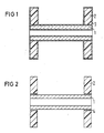
- the piezoceramic drive element is designed in the form of a so-called piezotube 1. Together with the holder 2, in the receiving openings of which the piezo tube 1 can be inserted, this forms the piezo module.
- the gap-free fastening can be done by covering the entire piezo module 1, 2 with a metallizable insulating layer 3, as shown in FIG. 1.
- a metallizable material 4 with adhesive properties, as shown in FIG. 2.
- This method is particularly suitable if the holder 2 consists of an insulating, metallizable plastic. In both cases, not only is a mechanically secure attachment ensured, but it is also ensured that the gap between the piezo tube 1 and the holder 2 is filled completely and without gaps.
- 3a to 3d show the further steps of the method according to the invention using a first exemplary embodiment.
- only one piezo tube 1 is shown, which together with the holder 2, into the openings of which the piezo tube 1 can be inserted, forms the piezo module.
- a piezo assembly actually consists of a multiplicity of piezo tubes which are inserted into corresponding openings in the holder.
- the entire piezo assembly 1, 2 is covered with a thin, metallizable insulating layer 3.
- a thin, metallizable insulating layer 3 By applying the insulating layer, the gap between the piezotube and the openings in the holder 2 is filled in a sealing manner and the piezotube is mechanically securely fastened.
- the entire piezo assembly 1, 2, 3 is then activated chemically or mechanically in a manner known per se and coated with a thin metal layer 5.
- 3a shows the piezo assembly after these steps.
- the contact surfaces for contacting the piezo tube 1 are then formed on the assembly covered with the metal layer 5.
- a cover is applied to the metal layer 5, the contours of which correspond to the later course of the conductor tracks and the contact connections.
- This can be done using the so-called positive technique or the so-called negative technique. In the positive technique, those areas of the piezo module that are later to be conductive are covered. In the negative technique, those areas are covered that will later isolate. Covering can be done by printing or by a photochemical process.
- the cover according to the negative technique is shown, ie a cover 6 covers all areas the piezo assembly, which later are insulating surfaces in the final state.
- the metal layer is reinforced in a further process step, which can be done, for example, by a galvanic process in a manner known per se. This creates the metal layer 7, as shown in Fig. 3b.
- the cover 6 is detached and the entire metal layer 5, 7 is detached or removed, for example by an etching process, to such an extent that the thin metal layer 5 is completely removed in the previously covered areas.
- the shape of the cover corresponds to their contours. An example of this is shown in FIGS. 3d and 3e.
- the metal layer 5 is reinforced before the cover is applied.
- the further metal layer is again designated 7.
- the areas of the piezo module that are not covered by a correspondingly shaped cover 8 are then subjected to a further treatment with which the entire metal layer 5, 7 is removed in these areas. This can be done by an etching process. The cover can then also be removed.
- the metal layer is mechanically removed at the locations which later have to be insulating in the final state in order to form the conductor tracks and the contact connections.
- An example of this is shown in FIG. 4.
- the holder 2 has corresponding elevations 9, on the surface of which, for example, by an automatic grinding process Metal layer 5 is removed.
- Metal layer 5 is removed.
- Fig. 5 shows a completely finished contacted piezo assembly for a multi-nozzle write head, which was produced according to the inventive method.
- the piezotubes 1 inserted into the holder 2 are provided on their inner and outer lateral surfaces with a metal layer 13, 14, which form the electrodes of the piezotubes 1.
- On the outer surface of the bracket 2 are 3a to 3b, the conductor tracks 11, 12 and the contact connections 10 are formed such that the inner electrode 13 of each piezo tube 1 can be controlled individually via a corresponding conductor track 11 and a corresponding contact connection 10, while the outer electrodes 14 of the Piezo tube 1 can be controlled together via the conductor track 11.
- the entire piezo assembly can be applied by applying a further outer protective layer in the form of a further thin insulating layer, which is applied in liquid or dissolved form under pressure, in an ultrasonic bath or by using centrifugal forces, both against external influences and against aggression Protect inks.
- the entire arrangement can then be cast.
Landscapes
- Particle Formation And Scattering Control In Inkjet Printers (AREA)
Applications Claiming Priority (6)
| Application Number | Priority Date | Filing Date | Title |
|---|---|---|---|
| DE3619859 | 1986-06-13 | ||
| DE19863619891 DE3619891A1 (de) | 1986-06-13 | 1986-06-13 | Verfahren zur vorbehandlung von piezokeramiken zum zwecke einer metallisierung |
| DE3619859 | 1986-06-13 | ||
| DE19863619925 DE3619925A1 (de) | 1986-06-13 | 1986-06-13 | Verfahren zum schutz von piezokeramischen antriebselementen |
| DE3619891 | 1986-06-13 | ||
| DE3619925 | 1986-06-13 |
Publications (2)
| Publication Number | Publication Date |
|---|---|
| EP0249221A2 true EP0249221A2 (fr) | 1987-12-16 |
| EP0249221A3 EP0249221A3 (fr) | 1989-10-04 |
Family
ID=27194492
Family Applications (1)
| Application Number | Title | Priority Date | Filing Date |
|---|---|---|---|
| EP87108401A Withdrawn EP0249221A3 (fr) | 1986-06-13 | 1987-06-10 | Méthode d'assemblage d'un module piézoélectrique à contacts pour tête d'enregistrement à jet d'encre |
Country Status (1)
| Country | Link |
|---|---|
| EP (1) | EP0249221A3 (fr) |
Cited By (1)
| Publication number | Priority date | Publication date | Assignee | Title |
|---|---|---|---|---|
| EP0693379A3 (fr) * | 1994-07-08 | 1997-03-12 | Nec Corp | Tête d'enregistrement à jet d'encre et sa méthode de fabrication |
Family Cites Families (2)
| Publication number | Priority date | Publication date | Assignee | Title |
|---|---|---|---|---|
| DE3324043A1 (de) * | 1983-07-04 | 1985-01-17 | Siemens AG, 1000 Berlin und 8000 München | Piezoelektrisches antriebselement fuer tintenmosaikschreibeinrichtung |
| US4493137A (en) * | 1983-09-19 | 1985-01-15 | Ncr Corporation | Method of making a drive element assembly for ink jet printing |
-
1987
- 1987-06-10 EP EP87108401A patent/EP0249221A3/fr not_active Withdrawn
Cited By (1)
| Publication number | Priority date | Publication date | Assignee | Title |
|---|---|---|---|---|
| EP0693379A3 (fr) * | 1994-07-08 | 1997-03-12 | Nec Corp | Tête d'enregistrement à jet d'encre et sa méthode de fabrication |
Also Published As
| Publication number | Publication date |
|---|---|
| EP0249221A3 (fr) | 1989-10-04 |
Similar Documents
| Publication | Publication Date | Title |
|---|---|---|
| DE69402850T2 (de) | Einseitiges antriebssystem verbindbar mit tintenstrahldruckkopf und dessen herstellungsverfahren | |
| EP0648607B1 (fr) | Module de tête à jet d'encre pour tête à jet d'encre éjectant de face et procédé pour sa fabrication | |
| DE69323978T2 (de) | Herstellungsverfahren eines Leiterrahmens | |
| DE3215608A1 (de) | Verfahren zum herstellen von duesenkanaelen und tintenstrahldrucker mit einem nach diesem verfahren hergestellten duesenkanal | |
| WO1989000373A1 (fr) | Procede de fabrication d'objets presentant des pistes conductiveset feuille a marquer utilisee pour mettre en oeuvre le procede | |
| DE19623070A1 (de) | Verfahren zum Herstellen einer Substratsanordnung für eine Flüssigkristallanzeigevorrichtung | |
| DE3532858A1 (de) | Verfahren zum anbringen von abschluessen an keramikkoerpern | |
| DE102013201926B4 (de) | Verfahren zum elektrischen Kontaktieren eines Bauteils und Bauteilverbund | |
| DE3138718A1 (de) | Halbleitervorrichtung und verfahren zu ihrer herstellung | |
| DE3403615A1 (de) | Schreibkopf fuer tintenschreibeinrichtungen | |
| DE4446509A1 (de) | Verfahren zur Herstellung von Leiterbahnen auf einem Vertiefungen aufweisenden Substrat | |
| DE3328598A1 (de) | Rueckschlagventil fuer einen nach bedarf tropfenweisen betreibbaren tintenstrahl-ejektor | |
| EP3111734A1 (fr) | Procédé de connexion électrique d'un composant incorporé dans un circuit imprimé ainsi que circuit imprimé | |
| CH667359A5 (de) | Verfahren zur herstellung einer starre und flexible partien aufweisenden leiterplatte fuer gedruckte elektrische schaltungen. | |
| DE69907525T2 (de) | Verfahren zur Herstellung eines Tintenstrahldruckkopfes und Tintenstrahldruckkopf | |
| DE69810799T2 (de) | Tröpfchenaufzeichnungsgerät und herstellungsverfahren | |
| DE4435914A1 (de) | Piezoelektrischer Antrieb für einen Tintenstrahldruckkopf und Verfahren zu dessen Herstellung | |
| EP0305318A1 (fr) | Procédé de fabrication des canaux d'encre dans une tête d'impression pour une imprimante matricielle à jet d'encre | |
| DE69514134T2 (de) | Tintenstrahldruckkopf | |
| EP0179452B1 (fr) | Procédé de fabrication de têtes d'impression pour mécanisme d'impression à encre | |
| EP0249221A2 (fr) | Méthode d'assemblage d'un module piézoélectrique à contacts pour tête d'enregistrement à jet d'encre | |
| WO2001037622A2 (fr) | Couche support de conducteurs imprimes destinee a etre inseree par laminage dans une carte a puce, procede de production de cette couche, moule de moulage par injection permettant de mettre en oeuvre le procede de production de cette couche support | |
| DE2360259A1 (de) | Gedruckte flachspule | |
| DE1145231B (de) | Verfahren zur Montage von Magnetkernspeichern | |
| DE3324043C2 (fr) |
Legal Events
| Date | Code | Title | Description |
|---|---|---|---|
| PUAI | Public reference made under article 153(3) epc to a published international application that has entered the european phase |
Free format text: ORIGINAL CODE: 0009012 |
|
| AK | Designated contracting states |
Kind code of ref document: A2 Designated state(s): CH DE ES FR GB IT LI NL SE |
|
| PUAL | Search report despatched |
Free format text: ORIGINAL CODE: 0009013 |
|
| AK | Designated contracting states |
Kind code of ref document: A3 Designated state(s): CH DE ES FR GB IT LI NL SE |
|
| 17P | Request for examination filed |
Effective date: 19891127 |
|
| STAA | Information on the status of an ep patent application or granted ep patent |
Free format text: STATUS: THE APPLICATION IS DEEMED TO BE WITHDRAWN |
|
| 18D | Application deemed to be withdrawn |
Effective date: 19910103 |
|
| RIN1 | Information on inventor provided before grant (corrected) |
Inventor name: MEINHOF, ANDRE-HEINRICH, DIPL.-ING. |