EP0248536A2 - Methoden und Gerät zum Suchen einer Zieladresse auf einem Aufzeichnungsmedium - Google Patents
Methoden und Gerät zum Suchen einer Zieladresse auf einem Aufzeichnungsmedium Download PDFInfo
- Publication number
- EP0248536A2 EP0248536A2 EP87304001A EP87304001A EP0248536A2 EP 0248536 A2 EP0248536 A2 EP 0248536A2 EP 87304001 A EP87304001 A EP 87304001A EP 87304001 A EP87304001 A EP 87304001A EP 0248536 A2 EP0248536 A2 EP 0248536A2
- Authority
- EP
- European Patent Office
- Prior art keywords
- address
- error check
- target address
- check code
- error
- Prior art date
- Legal status (The legal status is an assumption and is not a legal conclusion. Google has not performed a legal analysis and makes no representation as to the accuracy of the status listed.)
- Granted
Links
Images


Classifications
-
- G—PHYSICS
- G11—INFORMATION STORAGE
- G11B—INFORMATION STORAGE BASED ON RELATIVE MOVEMENT BETWEEN RECORD CARRIER AND TRANSDUCER
- G11B7/00—Recording or reproducing by optical means, e.g. recording using a thermal beam of optical radiation by modifying optical properties or the physical structure, reproducing using an optical beam at lower power by sensing optical properties; Record carriers therefor
- G11B7/08—Disposition or mounting of heads or light sources relatively to record carriers
- G11B7/085—Disposition or mounting of heads or light sources relatively to record carriers with provision for moving the light beam into, or out of, its operative position or across tracks, otherwise than during the transducing operation, e.g. for adjustment or preliminary positioning or track change or selection
- G11B7/08505—Methods for track change, selection or preliminary positioning by moving the head
-
- G—PHYSICS
- G11—INFORMATION STORAGE
- G11B—INFORMATION STORAGE BASED ON RELATIVE MOVEMENT BETWEEN RECORD CARRIER AND TRANSDUCER
- G11B27/00—Editing; Indexing; Addressing; Timing or synchronising; Monitoring; Measuring tape travel
- G11B27/10—Indexing; Addressing; Timing or synchronising; Measuring tape travel
-
- G—PHYSICS
- G11—INFORMATION STORAGE
- G11B—INFORMATION STORAGE BASED ON RELATIVE MOVEMENT BETWEEN RECORD CARRIER AND TRANSDUCER
- G11B20/00—Signal processing not specific to the method of recording or reproducing; Circuits therefor
- G11B20/10—Digital recording or reproducing
- G11B20/18—Error detection or correction; Testing, e.g. of drop-outs
- G11B20/1803—Error detection or correction; Testing, e.g. of drop-outs by redundancy in data representation
-
- G—PHYSICS
- G11—INFORMATION STORAGE
- G11B—INFORMATION STORAGE BASED ON RELATIVE MOVEMENT BETWEEN RECORD CARRIER AND TRANSDUCER
- G11B20/00—Signal processing not specific to the method of recording or reproducing; Circuits therefor
- G11B20/10—Digital recording or reproducing
- G11B20/18—Error detection or correction; Testing, e.g. of drop-outs
- G11B20/1806—Pulse code modulation systems for audio signals
- G11B20/1813—Pulse code modulation systems for audio signals by adding special bits or symbols to the coded information
-
- G—PHYSICS
- G11—INFORMATION STORAGE
- G11B—INFORMATION STORAGE BASED ON RELATIVE MOVEMENT BETWEEN RECORD CARRIER AND TRANSDUCER
- G11B21/00—Head arrangements not specific to the method of recording or reproducing
- G11B21/02—Driving or moving of heads
- G11B21/08—Track changing or selecting during transducing operation
- G11B21/081—Access to indexed tracks or parts of continuous track
- G11B21/083—Access to indexed tracks or parts of continuous track on discs
-
- G—PHYSICS
- G11—INFORMATION STORAGE
- G11B—INFORMATION STORAGE BASED ON RELATIVE MOVEMENT BETWEEN RECORD CARRIER AND TRANSDUCER
- G11B27/00—Editing; Indexing; Addressing; Timing or synchronising; Monitoring; Measuring tape travel
- G11B27/10—Indexing; Addressing; Timing or synchronising; Measuring tape travel
- G11B27/102—Programmed access in sequence to addressed parts of tracks of operating record carriers
- G11B27/105—Programmed access in sequence to addressed parts of tracks of operating record carriers of operating discs
-
- G—PHYSICS
- G11—INFORMATION STORAGE
- G11B—INFORMATION STORAGE BASED ON RELATIVE MOVEMENT BETWEEN RECORD CARRIER AND TRANSDUCER
- G11B27/00—Editing; Indexing; Addressing; Timing or synchronising; Monitoring; Measuring tape travel
- G11B27/10—Indexing; Addressing; Timing or synchronising; Measuring tape travel
- G11B27/19—Indexing; Addressing; Timing or synchronising; Measuring tape travel by using information detectable on the record carrier
- G11B27/28—Indexing; Addressing; Timing or synchronising; Measuring tape travel by using information detectable on the record carrier by using information signals recorded by the same method as the main recording
- G11B27/30—Indexing; Addressing; Timing or synchronising; Measuring tape travel by using information detectable on the record carrier by using information signals recorded by the same method as the main recording on the same track as the main recording
- G11B27/3027—Indexing; Addressing; Timing or synchronising; Measuring tape travel by using information detectable on the record carrier by using information signals recorded by the same method as the main recording on the same track as the main recording used signal is digitally coded
-
- G—PHYSICS
- G11—INFORMATION STORAGE
- G11B—INFORMATION STORAGE BASED ON RELATIVE MOVEMENT BETWEEN RECORD CARRIER AND TRANSDUCER
- G11B20/00—Signal processing not specific to the method of recording or reproducing; Circuits therefor
- G11B20/10—Digital recording or reproducing
- G11B2020/10916—Seeking data on the record carrier for preparing an access to a specific address
-
- G—PHYSICS
- G11—INFORMATION STORAGE
- G11B—INFORMATION STORAGE BASED ON RELATIVE MOVEMENT BETWEEN RECORD CARRIER AND TRANSDUCER
- G11B2220/00—Record carriers by type
- G11B2220/17—Card-like record carriers
-
- G—PHYSICS
- G11—INFORMATION STORAGE
- G11B—INFORMATION STORAGE BASED ON RELATIVE MOVEMENT BETWEEN RECORD CARRIER AND TRANSDUCER
- G11B2220/00—Record carriers by type
- G11B2220/20—Disc-shaped record carriers
-
- G—PHYSICS
- G11—INFORMATION STORAGE
- G11B—INFORMATION STORAGE BASED ON RELATIVE MOVEMENT BETWEEN RECORD CARRIER AND TRANSDUCER
- G11B2220/00—Record carriers by type
- G11B2220/20—Disc-shaped record carriers
- G11B2220/25—Disc-shaped record carriers characterised in that the disc is based on a specific recording technology
- G11B2220/2525—Magneto-optical [MO] discs
-
- G—PHYSICS
- G11—INFORMATION STORAGE
- G11B—INFORMATION STORAGE BASED ON RELATIVE MOVEMENT BETWEEN RECORD CARRIER AND TRANSDUCER
- G11B2220/00—Record carriers by type
- G11B2220/20—Disc-shaped record carriers
- G11B2220/25—Disc-shaped record carriers characterised in that the disc is based on a specific recording technology
- G11B2220/2537—Optical discs
-
- G—PHYSICS
- G11—INFORMATION STORAGE
- G11B—INFORMATION STORAGE BASED ON RELATIVE MOVEMENT BETWEEN RECORD CARRIER AND TRANSDUCER
- G11B27/00—Editing; Indexing; Addressing; Timing or synchronising; Monitoring; Measuring tape travel
- G11B27/10—Indexing; Addressing; Timing or synchronising; Measuring tape travel
- G11B27/102—Programmed access in sequence to addressed parts of tracks of operating record carriers
Definitions
- This invention relates to methods of and apparatus for seeking a target address on a record medium.
- an optical recording medium in the form of a disc such as an optical disc or an opto-magnetic disc
- spiral or concentric tracks are formed, with each track being divided into a plurality of sectors.
- an optical recording medium in the form of a card such as an optical card
- each band-like record area is divided into a plurality of record tracks.
- identification signals including error detection codes such as synchronization (sync) patterns, addresses or cyclic redundancy check (CRC) codes, as a result of pre-formatting by the card or disc supplier or formatting preceding the start of use of a new disc. It is by the address information included in the identification signals that a random access can be made to the recorded data on the record medium.
- the identification part of each block or sector in which are recorded these identification signals is also termed the ID part or the address part in the broad sense of the term.
- there are multiple writings for example three writings, of a unit of the identification information formed of an address consisting of a track address, a sector address and an error detection code (EDC) for detecting address errors.
- EDC error detection code
- the CRC code be replaced by an error correction code in order to deal with the higher error rates associated with optical discs.
- the pick-up head movement is controlled while checking the current address by reproducing the identification signals.
- a decoding operation such as the aforementioned error detection or correction operation is executed. This results in a complicated decoding process for error checking at the time of address reading or reproduction.
- the information unit when the information unit is formed by multiple recording or writing, it becomes necessary to determine the address by using, for example, a majority logic procedure after error detection or correction of each information unit, with a resulting complication in the hardware or the decoding algorithm, and prolonged computing time, thus presenting difficulties in achieving high speed accessing.
- a method of seeking a target address on a record medium on which are recorded data divided into a plurality of blocks in correlation with an address for each block and an error check code for each address comprising the steps of:
- a target address seeking apparatus for use with a signal reproducing means for reproducing signals recorded on a record medium on which recorded data are divided into a plurality of blocks in correlation with an address for each block and an error check code for each address: said target address seeking apparatus being characterized by:
- a target address seeking apparatus for use with a signal reproducing means for reproducing signals recorded on a record medium on which recorded data are divided into a plurality of blocks in correlation with an address for each block and an error check code for each address; said target address seeking apparatus comprising:
- the data to be recorded are divided into a plurality of blocks in correlation with an address for each block and an error check code for each address.
- the error check code to be appended to the target address is formed from the target address.
- the target address and the error check code are then compared with the address and the error check code which are read from the record medium. When it has become clear by such comparison that the error is within the range of the symbol or bit number that can be corrected by the error check code, the address read from the record medium is determined to be the target address.
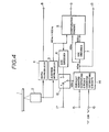
- Figure 1 illustrates a method of accessing a data block based on address seeking in accordance with an embodiment of the present invention.
- Signals are recorded on or reproduced from an optical disc 1, as an example of the recording medium, by an optical pick-up head 2.
- the signals from the pick-up head 2 are supplied to an address reading or reproducer circuit 3 where the address of the block or sector currently reproduced is read, and the thus read address signals are sent to a comparator circuit 5.
- These signals from the pick-up head 2 are also supplied to a data reproducer 4, so that data reproduced from the optical disc 1 are supplied to an output terminal 8.
- FIG. 2 An example of a proposed signal recording format for each block ,or sector on the optical disc 1 is shown in Figure. 2.
- a track on the optical disc 1 and an enlarged sector identification part or ID part are shown highly schematically.
- Each track consists of a plurality of sectors, with each sector consisting in turn of a pre-formatted identification part IDR and a data part DTR for recording the sector data.
- a sync signal PLOS for controlling the operation of a phase locked loop (PLL) circuit for producing clock signals at the time of data reading.
- PLOS phase locked loop
- Contiguous to this sync signal PLOS is a sector in which identifying address information UT is written three times in succession.
- Each unit UT1 to UT3 is formed by a leading sync pattern address mark SPA, an address AD consisting of a track address TA and a sector address SA and an error correction code ECC, consisting, for example of Bose-Chaudhuri-Hoquehem (BCH) codes, as address error check codes.
- ECC Error Correction code
- the track address TA is formed by sixteen bits while the sector address SA is formed by eight bits, so that the address is formed by a sum total of twenty-four bits.
- the length of the error correction code ECC is equal to the sum of the address data bits, and thus is set to twenty-four bits.
- the valid address For example, if the address data are formed by triple writing, the address data represented by two coincident data are adopted. This valid address is compared with the target address so that the pick-up head 2 is controlled to be shifted towards the block indicated by the target address.
- the current address cannot be determined until the totality of the addresses of the multiple units have been decoded for error checking.
- a continuous operation of time-consuming decoding is required, while the amount of hardware is also increased.
- the address error checking is performed by encoding the error check code based on the target address in lieu of decoding the target address data based on the error check code.
- a target address ADt supplied through an input terminal 6 from a host computer (not shown), for example, to the optical disc device is supplied to an error correction code (ECC) encoder 7 where the error correction code ECCt is appended to this address as the error check code.
- ECC error correction code
- the set comprising the target address ADt and the error correction code ECCt are supplied to the comparator circuit 5 for simple or bit-wise comparison with the set comprising the address and the error correction code included in the reproduced signal obtained at the address reproducer circuit 3.
- the reproduced address is determined to be the target address, so that a coincidence output is supplied to an output terminal 9.
- This coincidence output is used to control the accessing operation.
- Figure 3 is an example of the reproduced signal obtained upon reproduction of the signals recorded on the optical disc 1 in which the 24-bit error correction codes (ECC) as the error check codes, for example, are formed by triple writing or recording, similarly to the recording format of Figure 2.
- ECC error correction codes
- the sets of addresses and the error check codes making up the units UTI, UT2 and UT 3 formed by triple writing or recording are reproduced in the chronological order of AD1, ECCI, AD2, ECC2, AD3 and ECC3.
- the first step is to compare the set of AD1 and ECC with the set of the target address AD t and error correction code ECCt.
- the comparison operation at this point is a simple or bit-by-bit comparison.
- the block or sector corresponding to the address currently reproduced is determined to be the block corresponding to the aforementioned target block AD t.
- the target address seeking operation is controlled by judging whether the number of the faulty bits is coincident with or lesser than the aforementioned bit number a which is set as the allowable range or threshold value.
- ECC error correction code
- a (48, 24) enlarged BHC code formed by twenty-four bits can be employed. Since this code system has a minimum distance between the codes of twelve and an error correction capability of five bits, an error of a is less than or equal to four bits can be completely corrected.
- the reproduced address has been made coincident with the aforementioned target address by the seeking process when the symbol or bit error caused by bit-wise comparison is within a is less than or equal to four bits.
- the decoding operation which usually needs a complex algorithm and entails additional hardware may be omitted since it is possible to ascertain the reproduced address and access the desired block or sector by performing a decode operation using simpler hardware, without impairing the operational reliability.
- an error correction code such as a Reed Solomon code may be used in place of the BCH code.
- an allowable range or threshold of error for checking the coincidence of the read or reproduced signals which is different from that for checking the coincidence of the written or recorded signals.
- a threshold a for the reproduced or read signals a threshold ⁇ for the recorded or written signals can be selected to be less than the threshold a. This means that a narrower allowable range is used with more stringent coincidence conditions at the time of signal recording than at the time of signal reading or reproduction.
- the address currently reproduced may be determined to be the aforementioned target address only when a comparison difference within the threshold value a has been ascertained for the reproduced signals of at least k units of a total of n units formed by n-times recording or writing. In this case, it is unnecessary to wait until all of the n units have been reproduced, but the address currently reproduced can be instantly determined to be the aforementioned target address at the time the coincidence has been ascertained for the sequentially reproduced k units.
- the shifting of the optical pick-up head 2 until reaching the target address can be conventionally controlled.
- the difference between the read address value from the address reproducer circuit 3 and the target address value is determined by the comparator circuit 5 and a head driving actuator 12 is driven through a head driving control circuit 11 as a function of the difference so that the pick-up head 2 is moved through a head supporting plate 10 radially across the optical disc 1 or in the direction A, so that the difference between the reproduced address and the target address will become zero or a predetermined value.
- the address reproducer circuit 3 can be designed so that the address of the currently reproduced sector next to a preceding sector on the optical disc 1 is estimated by, for example, incrementing by " 1 " the reference address read from and determined for the preceding sector, the thus estimated address is compared with the actually reproduced address and the latter is supplied as the desired address when the compared addresses coincide with each other.
- an address reproducer circuit 3 may be employed in which the aforementioned estimated address is previously encoded and the thus encoded signal is compared with the reproduced address with an appended error check code and, when the symbol or bit error is within a prescribed tolerable range, the estimated address is recognized to be the desired address.
- FIG 4 is a block diagram showing the apparatus for address seeking in accordance with a modified embodiment of the present invention.
- the signals can be reproduced by an optical pick-up head 2 from the optical disc 1, as an example of the recording medium.
- the signals from the pick-up head 2 are supplied to the data reproducer 4 so that the data recorded on the optical disc 1 are supplied at the output terminal 8.
- the signals from the pick-up head 2 are also supplied to the address reproducer circuit 3 to be turned into corresponding digital signals.
- the identification part of the thus read digital signals (playback address ADPB and correction code EC CPB) is supplied to the comparator circuit 5.
- the address of the sector to be sought by the pick-up head 2 is estimated by an arithmetic operation carried out in a current address computing circuit 14 on the basis of the sector address ADre previously read from the optical disc 1 and determined to be valid.
- the estimated address ADes to be sought is subjected to encoding to find the error correction code ECCes.
- the set of the estimated address ADes and the code ECCes are compared bit-by-bit with the set of the playback address ADPB and the correction codes ECCPB obtained upon actual reproduction. When the symbol or bit error is within a prescribed range of the error correction capability of this error correcting code ECC, the address is determined to be valid.
- Figure 5 shows a plurality of sectors SEC1, SEC2, SEC3, .... contiguously formed on the optical disc 1.
- the addresses of the sectors SECI, SEC2, SEC3, .... are indicated by ADl, AD2, AD3, .... while the corresponding error correction codes are indicated by ECC1, ECC2, ECC3, ....
- the sector addresses and the corresponding error correction codes are shown to be formed only once for simplicity, they may also be formed by multiple recording, that is, they may be written a prescribed number of times, as shown in Figure 3.
- the error correction codes may also be replaced by an error detection code.
- an address of a desired sector such as an address AD1 of the section SEC1 shown in Figure 5, is read by the address reproducer circuit 3 shown in Figure 4.
- This address is decoded by an ECC decoder 26 using the error correction code ECC1 to find a reference address ADre having a higher reliability.
- This reference address is supplied from the ECC decoder 6 and is transmitted to the current address computing circuit (actually an address estimating circuit) 14 through a select terminal b of a changeover switch 18.
- the address of the sector SEC2 to be sought is computed or estimated on the basis of the reference address ADre in the address computing circuit 14 by the arithmetic operation of ADre+ 1 .
- the thus estimated address is then supplied to the ECC encoder 7 where it is subjected to error correction coding or encoding to derive the error correction code ECCes to be appended to the estimated address.
- the comparator circuit 5 supplies a coincidence signal at the output terminal 9.
- the address output signal is issued as a valid address via an output terminal 13 from the address computing circuit 14.
- the valid address output signal from the output terminal 13 is transmitted through, for example, an input terminal 17 to a select terminal a of the changeover switch 18, so as to be transmitted to the current address computing circuit 14 as the aforementioned reference address to be used for seeking the next sector address.
- the estimated address ADes can be computed by adding an addition data "1" from an input terminal 16 to the reference address ADre each time a sector count signal based on the disc rotation detection pulses or sector sync pulses obtained from the pick-up head 2 is supplied to an input terminal 15.
- the addition data to be supplied to the input terminal 16 is set to "n" and the additive operation is performed each time n sectors are counted, so that the estimated address will be transmitted to the comparator circuit 5.
- the comparison operation to be performed in the comparator circuit 5 may, for example, be a bit-by-bit comparison to find the number of the faulty symbols or bits.
- the block or sector that is currently reproduced is determined to be the block of the target address ADt.
- a check is made of whether the aforementioned faulty bit or symbol number is within the allowable range or threshold value in order to check for possible address coincidence.
- the reproduced address can be checked at high speed and with a high operational reliability compared to a conventional decode processing operation that requires in general a complicated algorithm and more hardware.
Landscapes
- Engineering & Computer Science (AREA)
- Signal Processing (AREA)
- Multimedia (AREA)
- Signal Processing For Digital Recording And Reproducing (AREA)
- Indexing, Searching, Synchronizing, And The Amount Of Synchronization Travel Of Record Carriers (AREA)
Priority Applications (1)
| Application Number | Priority Date | Filing Date | Title |
|---|---|---|---|
| AT87304001T ATE78627T1 (de) | 1986-05-31 | 1987-05-05 | Methoden und geraet zum suchen einer zieladresse auf einem aufzeichnungsmedium. |
Applications Claiming Priority (4)
| Application Number | Priority Date | Filing Date | Title |
|---|---|---|---|
| JP126006/86 | 1986-05-31 | ||
| JP61126006A JPS62283473A (ja) | 1986-05-31 | 1986-05-31 | ブロツクアクセス方法 |
| JP12600586A JPH0823991B2 (ja) | 1986-05-31 | 1986-05-31 | アドレス信号再生方法 |
| JP126005/86 | 1986-05-31 |
Publications (3)
| Publication Number | Publication Date |
|---|---|
| EP0248536A2 true EP0248536A2 (de) | 1987-12-09 |
| EP0248536A3 EP0248536A3 (en) | 1989-09-27 |
| EP0248536B1 EP0248536B1 (de) | 1992-07-22 |
Family
ID=26462284
Family Applications (1)
| Application Number | Title | Priority Date | Filing Date |
|---|---|---|---|
| EP87304001A Expired - Lifetime EP0248536B1 (de) | 1986-05-31 | 1987-05-05 | Methoden und Gerät zum Suchen einer Zieladresse auf einem Aufzeichnungsmedium |
Country Status (6)
| Country | Link |
|---|---|
| US (1) | US4800549A (de) |
| EP (1) | EP0248536B1 (de) |
| KR (1) | KR960001533B1 (de) |
| AU (1) | AU583188B2 (de) |
| CA (1) | CA1291562C (de) |
| DE (1) | DE3780517T2 (de) |
Cited By (16)
| Publication number | Priority date | Publication date | Assignee | Title |
|---|---|---|---|---|
| FR2619240A1 (fr) * | 1987-08-07 | 1989-02-10 | Toshiba Kk | Appareil de reproduction ou lecteur de disque et procede pour un acces rapide |
| WO1989006427A1 (en) * | 1988-01-06 | 1989-07-13 | Digital Equipment Corporation | Synchronization for stored data |
| EP0377340A3 (en) * | 1988-12-29 | 1990-11-22 | Sharp Kabushiki Kaisha | Recording/reproducing device |
| EP0378449A3 (en) * | 1989-01-13 | 1990-11-22 | Sharp Kabushiki Kaisha | Information recording and retrieval system |
| EP0376756A3 (en) * | 1988-12-29 | 1990-11-28 | Sharp Kk | Recording/reproducing device |
| EP0344994A3 (de) * | 1988-05-30 | 1991-01-30 | Sony Corporation | Antriebe für optische Platten |
| EP0349687A3 (de) * | 1987-07-07 | 1991-04-03 | Quantum Corporation | Verfahren und Einrichtung zur Kodierung der Sektoradressen einer magnetischen Platte |
| EP0335529A3 (de) * | 1988-03-31 | 1991-05-08 | Digital Equipment Corporation | Kodierungs- und Abbildungsverfahren und Gerät für Sektoradressen einer magnetischen Platte |
| EP0478323A3 (en) * | 1990-09-28 | 1992-05-27 | International Business Machines Corporation | Method of determining correctness and contents of control data structures in moving media data storage systems |
| USRE34003E (en) * | 1988-03-31 | 1992-07-21 | Digital Equipment Corporation | Method and apparatus for encoding and mapping magnetic disk sector addresses |
| US5237574A (en) * | 1988-04-08 | 1993-08-17 | Digital Equipment Corporation | Error-resilient information encoding |
| EP0461668A3 (en) * | 1990-06-15 | 1994-08-17 | Sony Corp | Data recording method |
| EP0553816A3 (en) * | 1992-01-28 | 1995-11-29 | Sony Corp | Disc shaped recording medium and address discrimination circuit for disc-shaped recording medium |
| WO2002021518A1 (en) * | 2000-09-01 | 2002-03-14 | Matsushita Electric Industrial Co., Ltd. | Optical disc medium, optical disc playback and recorder |
| US6724708B2 (en) | 2001-06-20 | 2004-04-20 | Matsushita Electric Industrial Co., Ltd. | Optical disk medium and method and apparatus for reading information |
| EP1139338A3 (de) * | 1994-03-19 | 2006-10-11 | Sony Corporation | Optische Platte und Verfahren und Gerät zur Aufzeichnung und Wiedergabe von dieser Platte |
Families Citing this family (20)
| Publication number | Priority date | Publication date | Assignee | Title |
|---|---|---|---|---|
| JP2526875B2 (ja) * | 1986-11-05 | 1996-08-21 | ソニー株式会社 | デイジタル情報記録装置 |
| US4964094A (en) * | 1987-07-15 | 1990-10-16 | Matsushita Electric Industrial Co., Ltd. | Optical disk |
| JPH087948B2 (ja) * | 1987-12-28 | 1996-01-29 | キヤノン株式会社 | 情報記録再生方法 |
| US5023876A (en) * | 1988-10-31 | 1991-06-11 | Pioneer Electronic Corporation | Method and apparatus for detecting finally recorded sector |
| JPH02199675A (ja) * | 1989-01-30 | 1990-08-08 | Pioneer Electron Corp | ディスク演奏装置 |
| US5130968A (en) * | 1989-02-21 | 1992-07-14 | Pioneer Electronic Corporation | Apparatus for monitoring a reading position for use in a disc player |
| GB2234107B (en) | 1989-07-20 | 1994-01-05 | Rowe International Inc | Control system for compact disc phonograph |
| JP2760077B2 (ja) * | 1989-08-29 | 1998-05-28 | ソニー株式会社 | 光ディスクのシーク回路 |
| US5428630A (en) * | 1993-07-01 | 1995-06-27 | Quantum Corp. | System and method for verifying the integrity of data written to a memory |
| US5602857A (en) * | 1993-09-21 | 1997-02-11 | Cirrus Logic, Inc. | Error correction method and apparatus |
| JP2920065B2 (ja) * | 1994-03-16 | 1999-07-19 | 株式会社東芝 | データ記録方法、記録装置、再生装置及び再生方法 |
| JPH0855462A (ja) * | 1994-08-11 | 1996-02-27 | Funai Techno Syst Kk | ヘッダのサーチ方法 |
| JP2001126408A (ja) * | 1999-10-29 | 2001-05-11 | Sony Corp | 光学式回転記録媒体、アドレス情報記録方法、アドレス情報復元方法、光学式記録装置、光学式再生装置、および、光学式記録・再生装置 |
| EP1178487A4 (de) * | 2000-02-10 | 2006-03-08 | Sony Corp | Verfahren zum aufzeichnen und/oder zur wiedergabe von daten auf/von ein/einem aufzeichnungsträger; wiedergabegerät, aufzeichnungsträger; verfahren zum erkennen von aufzeichnungsmedien mit bzw. ohne aufzeichnung und verfahren zum aufzeichnen und/oder zur wiedergabe von daten für geräte, die aufzeichnungsmedien mit bzw. ohne aufzeichnung verwenden |
| RU2284588C2 (ru) * | 2000-09-01 | 2006-09-27 | Мацусита Электрик Индастриал Ко., Лтд. | Носитель информации в виде оптического диска и устройство воспроизведения на оптическом диске |
| JP2002140875A (ja) * | 2000-11-01 | 2002-05-17 | Matsushita Electric Ind Co Ltd | ディスク再生装置およびディスク読み出し方法 |
| CN100354967C (zh) * | 2002-02-20 | 2007-12-12 | 索尼株式会社 | 用于记录介质的记录方法及装置、再现方法及装置、标识方法、以及数据传送方法及接收处理方法 |
| US20050219975A1 (en) * | 2002-06-28 | 2005-10-06 | Koninklijke Philips Electronics N.V. | Method and arrangement for the generation of an identification data block |
| US10528422B2 (en) * | 2017-11-13 | 2020-01-07 | Stmicroelectronics International N.V. | Redundant storage of error correction code (ECC) checkbits for validating proper operation of a static random access memory (SRAM) |
| US11861177B2 (en) * | 2021-08-06 | 2024-01-02 | Micron Technology, Inc. | Configurable verify level for a set of data in a memory device |
Family Cites Families (3)
| Publication number | Priority date | Publication date | Assignee | Title |
|---|---|---|---|---|
| JPS5913101B2 (ja) * | 1977-12-16 | 1984-03-27 | 株式会社日立製作所 | ランダムアクセス方法 |
| US4352131A (en) * | 1980-02-29 | 1982-09-28 | U.S. Philips Corporation | Memory disc addressing device |
| JPS59188815A (ja) * | 1983-04-08 | 1984-10-26 | Matsushita Electric Ind Co Ltd | 情報記録再生装置 |
-
1987
- 1987-05-05 EP EP87304001A patent/EP0248536B1/de not_active Expired - Lifetime
- 1987-05-05 DE DE8787304001T patent/DE3780517T2/de not_active Expired - Fee Related
- 1987-05-06 CA CA000536477A patent/CA1291562C/en not_active Expired - Lifetime
- 1987-05-06 US US07/047,699 patent/US4800549A/en not_active Expired - Lifetime
- 1987-05-21 AU AU73260/87A patent/AU583188B2/en not_active Ceased
- 1987-05-30 KR KR87005446A patent/KR960001533B1/ko not_active Expired - Fee Related
Cited By (37)
| Publication number | Priority date | Publication date | Assignee | Title |
|---|---|---|---|---|
| EP0349687A3 (de) * | 1987-07-07 | 1991-04-03 | Quantum Corporation | Verfahren und Einrichtung zur Kodierung der Sektoradressen einer magnetischen Platte |
| FR2619240A1 (fr) * | 1987-08-07 | 1989-02-10 | Toshiba Kk | Appareil de reproduction ou lecteur de disque et procede pour un acces rapide |
| WO1989006427A1 (en) * | 1988-01-06 | 1989-07-13 | Digital Equipment Corporation | Synchronization for stored data |
| US4914535A (en) * | 1988-01-06 | 1990-04-03 | Digital Equipment Corporation | Synchronization for stored data |
| EP0335529A3 (de) * | 1988-03-31 | 1991-05-08 | Digital Equipment Corporation | Kodierungs- und Abbildungsverfahren und Gerät für Sektoradressen einer magnetischen Platte |
| USRE34003E (en) * | 1988-03-31 | 1992-07-21 | Digital Equipment Corporation | Method and apparatus for encoding and mapping magnetic disk sector addresses |
| US5237574A (en) * | 1988-04-08 | 1993-08-17 | Digital Equipment Corporation | Error-resilient information encoding |
| EP0344994A3 (de) * | 1988-05-30 | 1991-01-30 | Sony Corporation | Antriebe für optische Platten |
| EP0377340A3 (en) * | 1988-12-29 | 1990-11-22 | Sharp Kabushiki Kaisha | Recording/reproducing device |
| EP0376756A3 (en) * | 1988-12-29 | 1990-11-28 | Sharp Kk | Recording/reproducing device |
| US5377167A (en) * | 1988-12-29 | 1994-12-27 | Sharp Kabushiki Kaisha | Recording/reproducing device |
| US5153861A (en) * | 1988-12-29 | 1992-10-06 | Sharp Kabushiki Kaisha | Recording/reproducing device |
| EP0378449A3 (en) * | 1989-01-13 | 1990-11-22 | Sharp Kabushiki Kaisha | Information recording and retrieval system |
| EP0461668A3 (en) * | 1990-06-15 | 1994-08-17 | Sony Corp | Data recording method |
| EP0727781A3 (de) * | 1990-06-15 | 1997-07-16 | Sony Corp | Datenaufzeichnungsverfahren |
| US5166935A (en) * | 1990-09-28 | 1992-11-24 | International Business Machines Corporation | Method of determining correctness and contents of control data structures in moving media data storage systems |
| EP0478323A3 (en) * | 1990-09-28 | 1992-05-27 | International Business Machines Corporation | Method of determining correctness and contents of control data structures in moving media data storage systems |
| EP0553816A3 (en) * | 1992-01-28 | 1995-11-29 | Sony Corp | Disc shaped recording medium and address discrimination circuit for disc-shaped recording medium |
| EP1139338A3 (de) * | 1994-03-19 | 2006-10-11 | Sony Corporation | Optische Platte und Verfahren und Gerät zur Aufzeichnung und Wiedergabe von dieser Platte |
| USRE42962E1 (en) | 1994-03-19 | 2011-11-22 | Sony Corporation | Optical disk and method and apparatus for recording and then playing information back from that disk |
| WO2002021518A1 (en) * | 2000-09-01 | 2002-03-14 | Matsushita Electric Industrial Co., Ltd. | Optical disc medium, optical disc playback and recorder |
| KR100796049B1 (ko) * | 2000-09-01 | 2008-01-21 | 마츠시타 덴끼 산교 가부시키가이샤 | 광디스크 매체, 광디스크 재생 방법 및 기록 방법 |
| US6608810B2 (en) | 2000-09-01 | 2003-08-19 | Matsushita Electric Industrial Co., Ltd. | Optical disk comprising a positional information section and a sync mark section each having a wobble pattern |
| US6757239B2 (en) | 2000-09-01 | 2004-06-29 | Matsushita Electric Industrial Co., Ltd. | Optical disk having wobble patterns and block identification marks |
| US7027374B2 (en) | 2000-09-01 | 2006-04-11 | Matsushita Electric Industrial Co., Ltd. | Optical disk having wobble patterns representing control information |
| US7075883B2 (en) | 2000-09-01 | 2006-07-11 | Matsushita Electric Industrial Co., Ltd. | Optical disk having wobble patterns representing control information |
| US7529167B2 (en) | 2000-09-01 | 2009-05-05 | Panasonic Corporation | Optical disk having wobble patterns representing control information |
| US6577590B2 (en) | 2000-09-01 | 2003-06-10 | Matsushita Electric Industrial Co., Ltd. | Optical disk having wobble patterns |
| US6674700B2 (en) | 2000-09-01 | 2004-01-06 | Matsushita Electric Industrial Co., Ltd. | Optical disk having sub-blocks and sub-block indentification marks |
| KR100798201B1 (ko) * | 2000-09-01 | 2008-01-24 | 마츠시타 덴끼 산교 가부시키가이샤 | 광디스크 매체, 광디스크 재생 장치, 재생 방법 및 기록 방법 |
| US7145843B2 (en) | 2000-09-01 | 2006-12-05 | Matsushita Electric Industrial Co., Ltd. | Optical disk having wobble patterns representing control information |
| US7362664B2 (en) | 2001-06-20 | 2008-04-22 | Matsushita Electric Industrial Co., Ltd. | Optical disk medium and method and apparatus for reading information |
| US7474607B2 (en) | 2001-06-20 | 2009-01-06 | Panasonic Corporation | Optical disk medium and method and apparatus for reading information |
| US7474606B2 (en) | 2001-06-20 | 2009-01-06 | Panasonic Corporation | Optical disk medium |
| US7116630B2 (en) | 2001-06-20 | 2006-10-03 | Matsushita Electric Industrial Co., Ltd. | Optical disk medium and method and apparatus for reading information |
| US7933170B2 (en) | 2001-06-20 | 2011-04-26 | Panasonic Corporation | Optical disk medium and method and apparatus for reading information |
| US6724708B2 (en) | 2001-06-20 | 2004-04-20 | Matsushita Electric Industrial Co., Ltd. | Optical disk medium and method and apparatus for reading information |
Also Published As
| Publication number | Publication date |
|---|---|
| US4800549A (en) | 1989-01-24 |
| AU583188B2 (en) | 1989-04-20 |
| DE3780517D1 (de) | 1992-08-27 |
| KR960001533B1 (en) | 1996-02-01 |
| KR870011607A (ko) | 1987-12-24 |
| EP0248536B1 (de) | 1992-07-22 |
| EP0248536A3 (en) | 1989-09-27 |
| CA1291562C (en) | 1991-10-29 |
| DE3780517T2 (de) | 1993-03-25 |
| AU7326087A (en) | 1987-12-03 |
Similar Documents
| Publication | Publication Date | Title |
|---|---|---|
| EP0248536B1 (de) | Methoden und Gerät zum Suchen einer Zieladresse auf einem Aufzeichnungsmedium | |
| US6981205B2 (en) | Data storage apparatus, read data processor, and read data processing method | |
| US5253131A (en) | Servo pattern for location and positioning of information on a disk drive | |
| US6288861B1 (en) | Disk drive with sector numbers encoded by sequences of sector types | |
| EP0349687B1 (de) | Verfahren und Einrichtung zur Kodierung der Sektoradressen einer magnetischen Platte | |
| KR100368958B1 (ko) | 위치 오차 신호 필드에 부호화된 정보를 갖는 디스크 드라이브 | |
| EP0353274B1 (de) | Synchronisierung für gespeicherte daten | |
| EP0272135A2 (de) | Optische Platte und optisches Plattengerät | |
| US6947364B1 (en) | Detecting track jumps during reading or writing of data on an optical disk | |
| US7131052B2 (en) | Algebraic decoder and method for correcting an arbitrary mixture of burst and random errors | |
| KR100304022B1 (ko) | 위치 오류 신호 필드에 부호화된 정보를 구비하는 데이터 기억 디스크 | |
| JP2508471B2 (ja) | アドレスデ−タの処理装置 | |
| JPH0724147B2 (ja) | 多重書きデ−タの復号方法 | |
| EP0411835B1 (de) | Dekodierungsanordnung | |
| JP2000048494A (ja) | ディスク記憶装置及び同装置におけるサーボセクタアドレスエラー検出方法 | |
| US20020194568A1 (en) | Error correcting method, disk medium, disk recording method and disk reproducing method | |
| JP3075922B2 (ja) | データ記録再生装置及び同装置に適用されるサーボ処理方法 | |
| JP3048616B2 (ja) | ディジタル再生装置 | |
| JPH025264A (ja) | 光情報記録再生装置のアドレス検出装置 | |
| JPH0693315B2 (ja) | ブロツクアクセス方法 | |
| JPH0823991B2 (ja) | アドレス信号再生方法 | |
| JPH0724145B2 (ja) | アドレス信号再生方法 | |
| JPH0693316B2 (ja) | ブロツクアクセス方法 | |
| JPS62283471A (ja) | アドレス信号再生方法 | |
| JPS6376154A (ja) | 同期信号の検出方式 |
Legal Events
| Date | Code | Title | Description |
|---|---|---|---|
| PUAI | Public reference made under article 153(3) epc to a published international application that has entered the european phase |
Free format text: ORIGINAL CODE: 0009012 |
|
| AK | Designated contracting states |
Kind code of ref document: A2 Designated state(s): AT DE FR GB IT NL |
|
| PUAL | Search report despatched |
Free format text: ORIGINAL CODE: 0009013 |
|
| AK | Designated contracting states |
Kind code of ref document: A3 Designated state(s): AT DE FR GB IT NL |
|
| 17P | Request for examination filed |
Effective date: 19900126 |
|
| 17Q | First examination report despatched |
Effective date: 19910524 |
|
| GRAA | (expected) grant |
Free format text: ORIGINAL CODE: 0009210 |
|
| ITF | It: translation for a ep patent filed | ||
| AK | Designated contracting states |
Kind code of ref document: B1 Designated state(s): AT DE FR GB IT NL |
|
| REF | Corresponds to: |
Ref document number: 78627 Country of ref document: AT Date of ref document: 19920815 Kind code of ref document: T |
|
| REF | Corresponds to: |
Ref document number: 3780517 Country of ref document: DE Date of ref document: 19920827 |
|
| ET | Fr: translation filed | ||
| PLBE | No opposition filed within time limit |
Free format text: ORIGINAL CODE: 0009261 |
|
| STAA | Information on the status of an ep patent application or granted ep patent |
Free format text: STATUS: NO OPPOSITION FILED WITHIN TIME LIMIT |
|
| 26N | No opposition filed | ||
| ITTA | It: last paid annual fee | ||
| REG | Reference to a national code |
Ref country code: GB Ref legal event code: IF02 |
|
| PGFP | Annual fee paid to national office [announced via postgrant information from national office to epo] |
Ref country code: GB Payment date: 20030430 Year of fee payment: 17 |
|
| PGFP | Annual fee paid to national office [announced via postgrant information from national office to epo] |
Ref country code: FR Payment date: 20030508 Year of fee payment: 17 |
|
| PGFP | Annual fee paid to national office [announced via postgrant information from national office to epo] |
Ref country code: AT Payment date: 20030514 Year of fee payment: 17 |
|
| PGFP | Annual fee paid to national office [announced via postgrant information from national office to epo] |
Ref country code: DE Payment date: 20030515 Year of fee payment: 17 |
|
| PGFP | Annual fee paid to national office [announced via postgrant information from national office to epo] |
Ref country code: NL Payment date: 20030530 Year of fee payment: 17 |
|
| PG25 | Lapsed in a contracting state [announced via postgrant information from national office to epo] |
Ref country code: GB Free format text: LAPSE BECAUSE OF NON-PAYMENT OF DUE FEES Effective date: 20040505 Ref country code: AT Free format text: LAPSE BECAUSE OF NON-PAYMENT OF DUE FEES Effective date: 20040505 |
|
| PG25 | Lapsed in a contracting state [announced via postgrant information from national office to epo] |
Ref country code: NL Free format text: LAPSE BECAUSE OF NON-PAYMENT OF DUE FEES Effective date: 20041201 Ref country code: DE Free format text: LAPSE BECAUSE OF NON-PAYMENT OF DUE FEES Effective date: 20041201 |
|
| GBPC | Gb: european patent ceased through non-payment of renewal fee |
Effective date: 20040505 |
|
| PG25 | Lapsed in a contracting state [announced via postgrant information from national office to epo] |
Ref country code: FR Free format text: LAPSE BECAUSE OF NON-PAYMENT OF DUE FEES Effective date: 20050131 |
|
| NLV4 | Nl: lapsed or anulled due to non-payment of the annual fee |
Effective date: 20041201 |
|
| REG | Reference to a national code |
Ref country code: FR Ref legal event code: ST |
|
| PG25 | Lapsed in a contracting state [announced via postgrant information from national office to epo] |
Ref country code: IT Free format text: LAPSE BECAUSE OF NON-PAYMENT OF DUE FEES;WARNING: LAPSES OF ITALIAN PATENTS WITH EFFECTIVE DATE BEFORE 2007 MAY HAVE OCCURRED AT ANY TIME BEFORE 2007. THE CORRECT EFFECTIVE DATE MAY BE DIFFERENT FROM THE ONE RECORDED. Effective date: 20050505 |