EP0246911A2 - Mehrstufiges elektrisches Signalverarbeitungsgerät - Google Patents
Mehrstufiges elektrisches Signalverarbeitungsgerät Download PDFInfo
- Publication number
- EP0246911A2 EP0246911A2 EP87304561A EP87304561A EP0246911A2 EP 0246911 A2 EP0246911 A2 EP 0246911A2 EP 87304561 A EP87304561 A EP 87304561A EP 87304561 A EP87304561 A EP 87304561A EP 0246911 A2 EP0246911 A2 EP 0246911A2
- Authority
- EP
- European Patent Office
- Prior art keywords
- signal processing
- electrical signal
- processing apparatus
- output
- intermediate result
- Prior art date
- Legal status (The legal status is an assumption and is not a legal conclusion. Google has not performed a legal analysis and makes no representation as to the accuracy of the status listed.)
- Granted
Links
Images


Classifications
-
- G—PHYSICS
- G06—COMPUTING OR CALCULATING; COUNTING
- G06F—ELECTRIC DIGITAL DATA PROCESSING
- G06F15/00—Digital computers in general; Data processing equipment in general
- G06F15/76—Architectures of general purpose stored program computers
- G06F15/80—Architectures of general purpose stored program computers comprising an array of processing units with common control, e.g. single instruction multiple data processors
- G06F15/8046—Systolic arrays
Definitions
- the invention relates to multistage electrical signal processing apparatus and particularly to such apparatus having processing elements distributed across a plurality of devices interconnected to form a cascaded array.
- Electrical signal processing apparatus including apparatus for analysing multi bit binary coded digital signals, is known including devices where a number of processing elements are provided on a single chip device such as an integrated circuit silicon chip. Such apparatus may require high speed sampling of data and difficulties arise when it is necessary to interconnect a number of such devices or chips in order to form a cascaded array. Electrical signals can be transferred more quickly in on-chip communication than off-chip communication which is necessary when data is communicated through a number of interconnected chips. Due to the small physical size of integrated circuit chips limited space is available for output and input pins to effect interchip connections and this can raise further difficulties in attempting to overcome slower off-chip communication in synchronous systolic arrays of processing elements partitioned across multiple devices when they are arranged to effect high frequency data sampling.
- the present invention provides multistage electrical signal processing apparatus comprising a plurality of signal processing elements distributed across a plurality of devices interconnected to form a cascaded array of devices, data supply means for inputting time varying input data to each of the processing elements, the same input data being supplied simultaneously to each of the devices, each device comprising:
- the apparatus includes means for updating the input data supplied to each of the elements in a succession of time controlled cycles so as to form in each device a new intermediate result in each cycle, said time delay means being arranged to introduce a time delay such that the intermediate result of a second device which is combined with the output of a first device is the intermediate result obtained from input data input to the second device during the cycle immediately following that of the formation of the intermediate result incorporated in the output of the first device.
- each device includes means effecting further time delay connected to said combining means and arranged to introduce a controlled time delay between generation of a said intermediate result by the element or elements or the device and the output of a combined result from the device thereby forming a time controlled pipeline in which combined outputs are output from the device at a frequency equal to that of said intermediate result formation but delayed by a controlled time delay.
- the combining means comprise adding devices for adding the output of one device to a said intermediate result of another device.
- other devices such as shifters, multipliers, or logical bit operators may be used as the combining means.
- the invention is particularly applicable to processing apparatus in which said elements each comprise adding devices connected in a chain and arranged to effect addition using input data and accumulation with an output from a preceding element.
- Each device may have a plurality of elements each comprising adding devices connected in a chain and each arranged to effect multiplication of input data with a coefficient and to accumulate the result of the multiplication with data output by a preceding element in the chain.
- the number of bits needed to represent the accumulated output of a succession of devices may increase as the number of devices included in the array increases. It may therefore be desirable to output from each device to the next fewer bits than are used to represent the accumulated output of the said device.
- the elements are arranged to process multi bit binary coded digital signals, each device including selector means for selecting from said intermediate results a signal formed by less bits than the multi bit signal processed by each element.
- connection having a bit width with less bits than the multi bit signals processed by each element.
- the invention is particularly applicable to a transversal filter for effecting electrical signal analysis, said filter comprising a cascaded array of separate filter devices. Each such device may comprise a single silicon chip.
- This particular example relates to digital transversal filters in which a synchronous systolic array is formed by interconnecting a plurality of single integrated circuit chip devices, each chip having N stages of filtering.
- Each stage of the filter is arranged to multiply input data, which in this example is represented by a l6 bit number, by a stage coefficient which in this example is represented by a further l6 bit number.
- Each stage effects this multiplication in a time controlled major cycle consisting of a plurality of minor cycles, each minor cycle involving the formation of a partial product and addition with any previous partial products of that major cycle.
- the input data is fed simultaneously to all devices and to all stages on each device.
- the input data is updated each major cycle.
- the major cycle has a time T and after each major cycle the output of each stage is fed to the next stage on the same chip and a new product calculation is commenced using new updated input data.
- FIG. l The arrangement shown in Figure l is provided on a single chip and in this example consists of thirty two successive stages of which only the first two stages l2 and l3 and the final stage l4 have been marked.
- the operation of each stage is carried out under the control of a control unit l5 using input data derived from an input shift register l6.
- Each stage includes thirty six bit locations each having an adder for use in forming and accumulating partial products for each minor cycle.
- the adders in each stage need not complete resolution of any carry signals during each major cycle.
- Each stage forwards a sum and carry signal to the next stage after completion of each major cycle and the last stage l4 provides an output consisting of sum and carry signals for each bit position to a carry propagate adder l7.
- FIG. 2 illustrates a clock pulse train 2l derived from a clock 20 and in the examples shown one clock pulse is required for each minor cycle used in partial product formation.
- each major cycle consists of four successive clock pulses which would be appropriate for a four or eight bit coefficient.
- the input data supplied into the shift register l6 is illustrated at 22 and this may incorporate a signal to indicate periods when the data is valid and may properly be sampled.
- the device of Figure l is arranged to sample input data on a rising edge of a clock pulse so that data for two successive major cycles is sampled at the instances marked 23 and 24 in Figure 2.
- FIG. 3 Such a cascade is illustrated in Figure 3 although this example is not in accordance with the invention.
- Each device incorporates a plurality of stages 34 and the operation of each is controlled by a common clock giving clock pulse inputs 35.
- Such devices may be arranged to operate at particularly high speed. For example the input data may be cycled at frequencies up to l0 MHz. Signal transfer is effected much more quickly in on-chip communication than in off-chip communication.
- each stage on any one chip is connected to the next stage by high speed on-chip connections but the output of the last stage on device 30 is connected directly to an input to the first stage 34 on chip 3l by an external off-chip connection 36.
- This off-chip connection 36 will be a multi bit parallel connection depending on the bit width of the output signal to be conveyed from each chip to the next. It will inevitably be slower than the on-chip communication and in high speed operation it will not be possible for the output from the device 30 to be received for processing by the first stage 34 of the second device 3l in synchronism with a major cycle of operation on device 3l following immediately after the previous major cycle in which the last stage on device 30 formed an output.
- This unavoidable delay in line 36 would mean introducing some form of delay into the input data line 32 which would therefore require additional input pins on each device to receive the delayed output from the delay device in the input data bus 32.
- the necessary number of bits in the interchip connection 36 will require an extra bit for each doubling in the number of filter stages 34 which are involved in the cascaded array.
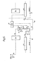
- FIG 4 shows a modification of the cascaded arrangement which is in accordance with the present invention.
- Each chip in this example comprises a CMOS chip having N stages of filter each stage being marked 34.
- the filter stages are controlled by a control unit l5 using a timing clock 20 as previously described with reference to Figure l.
- An intermediate result l8 is formed for each device by the adder l7.
- the output 40 from the adder l7 is fed to a selector and rounder 4l before reaching a combination device in the form of a carry propagate adder 42.
- the adder 42 combines the output 43 from the selector 4l with the output 44 from a delay shift register 45.
- the adders l7 and 42 as well as the selector 4l and shift register 45 are controlled by the clock 20.
- the adder 42 provides a combined output 46 which is fed through a multi bit parallel data path 48 to the input 49 of the next device in the cascade.
- the input 49 is connected to the input of the delay shift register 45 in the next device.
- the connection between the two devices is illustrated more fully in Figure 5 which shows the output part of a device 30 and the input part of device 3l.
- Figure 5 uses a notation on the data buses showing the bit width of the data paths.
- the DATAIN line 32 provides a l6 bit signal to the filter stages and the output of the last filter stage 34 on each device is a thirty six bit signal fed to the adder l7.
- the intermediate result from the adder l7 is formed on line 40 which in this example is still a thirty six bit signal.
- the selector 4l selects the most significant twenty one bits and has a carry in from the most significant discarded bit so that rounding is achieved. It provides an output on line 43 which is a twenty four bit signal and the most significant three bit locations have sign extension so as to contain the same bits as the most significant bit of the twenty one selected bits. This allows the apparatus to operate in two's complement in order to handle negative numbers.
- the twenty four bit signal on line 43 is fed to the adder 42 where the signal is combined with any output on line 44 from the delay register 45.
- the signal on line 44 is also a twenty four bit signal and a twenty four bit output is provided on line 48 which interconnects the output of the first device 30 to the input of the delay register 45 on the second device 3l. It will therefore be seen that the signal which forms the combined output from any one device is fed along line 48 through the delay register 45 on the next device so that it is combined with the intermediate output of the next device in the cascaded array.
- the adders l7 and 42 as well as the selector 4l will each take time to carry out their respective operations and as they are controlled by the clock 20 they are allocated an integral number of major cycles in which to operate. For this example it is assumed that the adder l7 and selector 4l introduce a delay of P major cycles.
- the adder 42 may incorporate additional time delay illustrated at 49 so that the combined delay of operation of the adder 42 together with inherent delay in the off-chip communication 48 represents a whole number of major cycles between the adder 42 and the input to the delay register 45 on the second device. It is assumed that this collective delay between the adder 42 and the input to the shift register 45 on the next device is represented by X major cycles.
- the time of processing by the N stages on each chip is N major cycles.
- the combined output 46 from any one chip is joined at the adder 42 of the next chip with the intermediate result of the next chip in such a way that the two are time synchronised.
- the intermediate result at the second chip will have been derived using input data which was input to the second chip immediately following the last major cycle in which data was input to the first chip in forming the combined output from the first chip.
- This enables synchronism between the chips to be achieved without causing any delay in the DATAIN supply to each of the chips. It permits reduction in the number of bits transmitted through the interconnection 48 between successive chips so that less input and output pins are necessary on the restricted space available on each chip.
- the use of twenty four bits only twenty one of which are used prior to sign extension by the selector 4l on the first chip allows for additional bits to be included after each doubling of the number of filter stages in the cascade. By arranging for the rounded output of each stage to be combined only with the rounded output of the next stage, less inaccuracy results as the second device does not itself carry out rounding on a number which has already been rounded by a previous stage.
- the delay of P major cycles introduced by the adder l7 and selector 4l is common to each chip and need not be taken into account in determining the number of delay units to be introduced by the shift register 45.
- the invention is not limited to the details of the foregoing example. For instance, if the delay of P units introduced after the last stage of each device prior to combination at the adder 42 is not common to each unit then variation in the delay achieved by the shift registezr 45 will be necessary to achieve synchronism of the output of one device with the intermediate result of the next device.
Landscapes
- Engineering & Computer Science (AREA)
- Computer Hardware Design (AREA)
- Theoretical Computer Science (AREA)
- Computing Systems (AREA)
- Physics & Mathematics (AREA)
- General Engineering & Computer Science (AREA)
- General Physics & Mathematics (AREA)
- Complex Calculations (AREA)
- Filters That Use Time-Delay Elements (AREA)
Applications Claiming Priority (2)
| Application Number | Priority Date | Filing Date | Title |
|---|---|---|---|
| GB868612455A GB8612455D0 (en) | 1986-05-22 | 1986-05-22 | Signal processing apparatus |
| GB8612455 | 1986-05-22 |
Publications (3)
| Publication Number | Publication Date |
|---|---|
| EP0246911A2 true EP0246911A2 (de) | 1987-11-25 |
| EP0246911A3 EP0246911A3 (en) | 1989-09-27 |
| EP0246911B1 EP0246911B1 (de) | 1992-11-11 |
Family
ID=10598263
Family Applications (1)
| Application Number | Title | Priority Date | Filing Date |
|---|---|---|---|
| EP87304561A Expired EP0246911B1 (de) | 1986-05-22 | 1987-05-21 | Mehrstufiges elektrisches Signalverarbeitungsgerät |
Country Status (5)
| Country | Link |
|---|---|
| US (1) | US4835725A (de) |
| EP (1) | EP0246911B1 (de) |
| JP (1) | JPH0831773B2 (de) |
| DE (1) | DE3782538T2 (de) |
| GB (1) | GB8612455D0 (de) |
Cited By (1)
| Publication number | Priority date | Publication date | Assignee | Title |
|---|---|---|---|---|
| EP0636992A1 (de) * | 1993-07-14 | 1995-02-01 | Matsushita Electric Industrial Co., Ltd. | Pipeline-Rechner |
Families Citing this family (10)
| Publication number | Priority date | Publication date | Assignee | Title |
|---|---|---|---|---|
| GB8612455D0 (en) | 1986-05-22 | 1986-07-02 | Inmos Ltd | Signal processing apparatus |
| US5140688A (en) * | 1986-11-10 | 1992-08-18 | Texas Instruments Incorporated | GaAs integrated circuit programmable delay line element |
| US5068813A (en) * | 1989-11-07 | 1991-11-26 | Mts Systems Corporation | Phased digital filtering in multichannel environment |
| JP2541044B2 (ja) * | 1991-08-29 | 1996-10-09 | 真作 森 | 適応フィルタ装置 |
| US5440721A (en) * | 1992-03-24 | 1995-08-08 | Sony Electronics, Inc. | Method and apparatus for controlling signal timing of cascaded signal processing units |
| FI96256C (fi) * | 1993-04-05 | 1996-05-27 | Tapio Antero Saramaeki | Menetelmä ja järjestely transponoidussa digitaalisessa FIR-suodattimessa binäärisen sisääntulosignaalin kertomiseksi tappikertoimilla sekä menetelmä transponoidun digitaalisen suodattimen suunnittelemiseksi |
| TW290769B (de) * | 1994-11-15 | 1996-11-11 | Matsushita Electric Industrial Co Ltd | |
| JP4671882B2 (ja) * | 2006-02-13 | 2011-04-20 | ソニー株式会社 | 演算装置および並列演算装置 |
| JP4737248B2 (ja) * | 2008-08-11 | 2011-07-27 | ソニー株式会社 | 演算装置および並列演算装置 |
| JP5303594B2 (ja) * | 2011-03-29 | 2013-10-02 | アンリツ株式会社 | 周波数変換装置 |
Family Cites Families (6)
| Publication number | Priority date | Publication date | Assignee | Title |
|---|---|---|---|---|
| US3665171A (en) * | 1970-12-14 | 1972-05-23 | Bell Telephone Labor Inc | Nonrecursive digital filter apparatus employing delayedadd configuration |
| FR2250240B1 (de) * | 1973-10-23 | 1976-07-02 | Ibm France | |
| US4507725A (en) * | 1982-07-01 | 1985-03-26 | Rca Corporation | Digital filter overflow sensor |
| GB8429879D0 (en) * | 1984-11-27 | 1985-01-03 | Rca Corp | Signal processing apparatus |
| US4773034A (en) * | 1985-05-09 | 1988-09-20 | American Telephone And Telegraph Company | Adaptive equalizer utilizing a plurality of multiplier-accumulator devices |
| GB8612455D0 (en) | 1986-05-22 | 1986-07-02 | Inmos Ltd | Signal processing apparatus |
-
1986
- 1986-05-22 GB GB868612455A patent/GB8612455D0/en active Pending
-
1987
- 1987-05-19 US US07/052,248 patent/US4835725A/en not_active Expired - Lifetime
- 1987-05-21 EP EP87304561A patent/EP0246911B1/de not_active Expired
- 1987-05-21 DE DE8787304561T patent/DE3782538T2/de not_active Expired - Fee Related
- 1987-05-22 JP JP62125668A patent/JPH0831773B2/ja not_active Expired - Lifetime
Cited By (1)
| Publication number | Priority date | Publication date | Assignee | Title |
|---|---|---|---|---|
| EP0636992A1 (de) * | 1993-07-14 | 1995-02-01 | Matsushita Electric Industrial Co., Ltd. | Pipeline-Rechner |
Also Published As
| Publication number | Publication date |
|---|---|
| JPH0831773B2 (ja) | 1996-03-27 |
| GB8612455D0 (en) | 1986-07-02 |
| EP0246911B1 (de) | 1992-11-11 |
| EP0246911A3 (en) | 1989-09-27 |
| DE3782538D1 (de) | 1992-12-17 |
| DE3782538T2 (de) | 1993-04-15 |
| JPS62286306A (ja) | 1987-12-12 |
| US4835725A (en) | 1989-05-30 |
Similar Documents
| Publication | Publication Date | Title |
|---|---|---|
| EP0253475B1 (de) | Mehrstufiges Multiplizier- und Addiergerät für Digitalsignale | |
| US5005120A (en) | Compensating time delay in filtering signals of multi-dimensional reconvigurable array processors | |
| EP0137464A2 (de) | Digitale Signalverarbeitungseinrichtung mit einem digitalen Filter | |
| US4791600A (en) | Digital pipelined heterodyne circuit | |
| EP0246911B1 (de) | Mehrstufiges elektrisches Signalverarbeitungsgerät | |
| EP0583927A1 (de) | Dynamisches adaptives Entzerrersystem und Verfahren hierfür | |
| US4021616A (en) | Interpolating rate multiplier | |
| US5805479A (en) | Apparatus and method for filtering digital signals | |
| US4760540A (en) | Adaptive interference cancelling system and method | |
| US3959639A (en) | Calculating unit for serial multiplication including a shift register and change-over switching controlling the transmission of the multiplicand bits to form the product | |
| EP0281325A1 (de) | Einrichtung und Verfahren zum Unterbrechungshinweis | |
| US5005149A (en) | Digital computation integrated circuit for convolution type computations | |
| EP1703636B1 (de) | Fir-filter | |
| JPH0834407B2 (ja) | 入力加重形トランスバーサルフィルタ | |
| JPH0322725B2 (de) | ||
| GB2226899A (en) | An electronic circuit and signal processing arrangements using it | |
| JPS621312A (ja) | デイジタルフイルタ | |
| EP2085893A2 (de) | Signalprozessor | |
| SU947860A1 (ru) | Устройство дл умножени по модулю | |
| US6772358B1 (en) | System and method for coordinating activation of a plurality of modules through the use of synchronization cells comprising a latch and regulating circuits | |
| JP2580641B2 (ja) | ブロック同期回路 | |
| JPS59103143A (ja) | 多重化演算方式 | |
| JPH01268306A (ja) | 入力加重型トランスバーサルフィルタ | |
| JP2001036382A (ja) | Iirデジタルフィルタ | |
| JPS61121172A (ja) | 位相分割処理方式 |
Legal Events
| Date | Code | Title | Description |
|---|---|---|---|
| PUAI | Public reference made under article 153(3) epc to a published international application that has entered the european phase |
Free format text: ORIGINAL CODE: 0009012 |
|
| AK | Designated contracting states |
Kind code of ref document: A2 Designated state(s): DE FR GB IT NL |
|
| PUAL | Search report despatched |
Free format text: ORIGINAL CODE: 0009013 |
|
| AK | Designated contracting states |
Kind code of ref document: A3 Designated state(s): DE FR GB IT NL |
|
| 17P | Request for examination filed |
Effective date: 19890925 |
|
| 17Q | First examination report despatched |
Effective date: 19910422 |
|
| ITTA | It: last paid annual fee | ||
| ITF | It: translation for a ep patent filed | ||
| GRAA | (expected) grant |
Free format text: ORIGINAL CODE: 0009210 |
|
| AK | Designated contracting states |
Kind code of ref document: B1 Designated state(s): DE FR GB IT NL |
|
| PG25 | Lapsed in a contracting state [announced via postgrant information from national office to epo] |
Ref country code: NL Effective date: 19921111 |
|
| REF | Corresponds to: |
Ref document number: 3782538 Country of ref document: DE Date of ref document: 19921217 |
|
| ET | Fr: translation filed | ||
| NLV1 | Nl: lapsed or annulled due to failure to fulfill the requirements of art. 29p and 29m of the patents act | ||
| PLBE | No opposition filed within time limit |
Free format text: ORIGINAL CODE: 0009261 |
|
| STAA | Information on the status of an ep patent application or granted ep patent |
Free format text: STATUS: NO OPPOSITION FILED WITHIN TIME LIMIT |
|
| 26N | No opposition filed | ||
| REG | Reference to a national code |
Ref country code: FR Ref legal event code: TP |
|
| REG | Reference to a national code |
Ref country code: GB Ref legal event code: 732E |
|
| REG | Reference to a national code |
Ref country code: FR Ref legal event code: D6 |
|
| PGFP | Annual fee paid to national office [announced via postgrant information from national office to epo] |
Ref country code: DE Payment date: 20010514 Year of fee payment: 15 |
|
| REG | Reference to a national code |
Ref country code: GB Ref legal event code: IF02 |
|
| PGFP | Annual fee paid to national office [announced via postgrant information from national office to epo] |
Ref country code: GB Payment date: 20020522 Year of fee payment: 16 |
|
| PGFP | Annual fee paid to national office [announced via postgrant information from national office to epo] |
Ref country code: FR Payment date: 20020527 Year of fee payment: 16 |
|
| PG25 | Lapsed in a contracting state [announced via postgrant information from national office to epo] |
Ref country code: DE Free format text: LAPSE BECAUSE OF NON-PAYMENT OF DUE FEES Effective date: 20021203 |
|
| PG25 | Lapsed in a contracting state [announced via postgrant information from national office to epo] |
Ref country code: GB Free format text: LAPSE BECAUSE OF NON-PAYMENT OF DUE FEES Effective date: 20030521 |
|
| GBPC | Gb: european patent ceased through non-payment of renewal fee |
Effective date: 20030521 |
|
| PG25 | Lapsed in a contracting state [announced via postgrant information from national office to epo] |
Ref country code: FR Free format text: LAPSE BECAUSE OF NON-PAYMENT OF DUE FEES Effective date: 20040130 |
|
| REG | Reference to a national code |
Ref country code: FR Ref legal event code: ST |
|
| PG25 | Lapsed in a contracting state [announced via postgrant information from national office to epo] |
Ref country code: IT Free format text: LAPSE BECAUSE OF NON-PAYMENT OF DUE FEES;WARNING: LAPSES OF ITALIAN PATENTS WITH EFFECTIVE DATE BEFORE 2007 MAY HAVE OCCURRED AT ANY TIME BEFORE 2007. THE CORRECT EFFECTIVE DATE MAY BE DIFFERENT FROM THE ONE RECORDED. Effective date: 20050521 |