EP0243988B1 - Verfahren zur Herstellung einer Halbleiteranordnung - Google Patents
Verfahren zur Herstellung einer Halbleiteranordnung Download PDFInfo
- Publication number
- EP0243988B1 EP0243988B1 EP87200372A EP87200372A EP0243988B1 EP 0243988 B1 EP0243988 B1 EP 0243988B1 EP 87200372 A EP87200372 A EP 87200372A EP 87200372 A EP87200372 A EP 87200372A EP 0243988 B1 EP0243988 B1 EP 0243988B1
- Authority
- EP
- European Patent Office
- Prior art keywords
- opening
- electrode zone
- pattern
- zone
- layer
- Prior art date
- Legal status (The legal status is an assumption and is not a legal conclusion. Google has not performed a legal analysis and makes no representation as to the accuracy of the status listed.)
- Expired
Links
Images


Classifications
-
- H10W20/069—
-
- H10P76/40—
-
- Y—GENERAL TAGGING OF NEW TECHNOLOGICAL DEVELOPMENTS; GENERAL TAGGING OF CROSS-SECTIONAL TECHNOLOGIES SPANNING OVER SEVERAL SECTIONS OF THE IPC; TECHNICAL SUBJECTS COVERED BY FORMER USPC CROSS-REFERENCE ART COLLECTIONS [XRACs] AND DIGESTS
- Y10—TECHNICAL SUBJECTS COVERED BY FORMER USPC
- Y10S—TECHNICAL SUBJECTS COVERED BY FORMER USPC CROSS-REFERENCE ART COLLECTIONS [XRACs] AND DIGESTS
- Y10S148/00—Metal treatment
- Y10S148/011—Bipolar transistors
Definitions
- the invention relates to a method of manufacturing an integrated circuit comprising a semiconductor body having a surface adjoined by a first and a second surface region, the first surface region being of a first conductivity type and being intended to accomodate at least one field effect transistor having an insulation gate, a source and a drain zone of the second conductivity type and the second surface region being intended to accomodate at least one further circuit elements having a first electrode zone which adjoins the surface and occupies a first surface portion of the surface, as well as a second electrode zone which adjoins the surface in the first surface portion and which has a conductivity type opposite to that of the first electrode zone, a pattern of conductive material being provided on an already present first insulating layer above at least a part of the first electrode zone simultaneously with the gate electrode of the field effect transistor, which pattern defines at least a first part of the edge of a first opening to be used in a first doping treatment for providing a dopant for the second electrode zone, in which a part of the first insulating layer located in the first
- Such a method is known from Federal German Patent Application (DE-A) 3023616, which has been laid open to public inspection on January 22 nd 1981.
- a lateral bipolar transistor is formed, whose base zone constitutes the first electrode zone and whose emitter zone constitutes the second electrode zone, while the part of the base zone located between the emitter zone and the collector zone is covered with a conductive pattern, which is located on an insulating layer, surrounds the emitter zone like a ring and may be connected to the electrical connection of the emitter zone.
- the conductive pattern serves to reduce the recombination of charge carriers at the surface in the subjacent part of the base zone.
- the bipolar transistor is manufactured thus in order that the electrical connections of the emitter zone and of the collector zone can be provided at a comparatively small relative distance and nevertheless a conductive layer can be formed at the same time above the said part of the base zone. Due to the fact that the emitter and/or the collector connections can overlap the conductive pattern located above this base zone, an area saving is obtained in this structure.
- the present invention has inter alia for its object to indicate how during the manufacture of integrated circuits comprising field effect transistors and in bipolar circuit elements, more particularly bipolar transistors, comparatively small electrode zones can be used in these bipolar circuit elements.
- an opening in an insulating layer is first used as a doping opening for providing the dopant for the relevant small electrode zone in the semiconductor body and is then also used as a contact opening for connecting the electrical connection for this electrode zone which is provided in the form of a conductive layer, to this electrode zone.
- the usual alignment tolerance with respect to the doping opening need not be taken into account for the provision of the contact opening.
- This method is used, for example, in so-called "washed-out" emitters.
- the gate electrode is employed as a masking when the dopant for the source and drain zones is provided.
- contact openings are provided above the source and drain zones by means of a mask.
- these integrated circuits also include bipolar circuit elements having an electrode zone which is provided simultaneously with the source and drain zones, also in this circuit element the pattern for the contact opening has to be aligned with respect to the relevant electrode zone. The method described above and used with "washed-out" emitters is consequently not suitable to be used in this process.
- the present invention has inter alia also for its object to avoid at least to a considerable extent the aforementioned disadvantages associated with the use of comparatively small electrode zones. It is based inter alia on the recognition of the fact that also in a method in which gate electrodes are employed in a usual manner as a masking during the step of providing the doping for source and drain zones in bipolar circuit elements, such as bipolar transistors, where required, the alignment tolerance for providing contact openings can practically be eliminated.
- a method of the kind described in the opening paragraph is characterized in that during the step of locally removing the second layer a second opening is located above the second electrode zone in such a manner that the first part of the edge of the first opening is located at least in part within the second opening, in that this step of locally removing the second insulating layer is carried out by anisotropic etching in such a manner that an edge portion of the second insulating layer located along the part of the edge of the pattern disposed within the second opening is left in the first opening, after which the conductive layer is provided in such a manner that the second surface part extends practically to the edge of the first opening at the area at which this edge is located within the second opening.
- a conductive pattern separated by an insulating layer from the first electrode zone is provided in the further circuit element, which is mostly a bipolar circuit element.
- This conductive pattern is used to define, where required, a part of the boundary or the whole boundary of a doping opening for providing the second electrode zone.
- the contact opening for the second electrode zone is derived from the boundary of the doping opening defined by the pattern in that a deposited insulating layer is removed locally by anisotropic etching in such a manner that edge portions of this insulating layer are left along the said boundary.
- the contact opening is derived from the doping opening, it is avoided that for this contact opening an alignment tolerance with respect to the doping opening has to be taken into account. Moreover, the advantage is obtained that the contact opening is smaller than the doping opening. As a result, pn junctions located at a very small depth will also remain satisfactorily passivated when the conductive connection for the second electrode zone is provided.
- the contact opening in situ has practically the same size as the doping opening.
- the term "practically the same size" indicates that the contact opening is derived in situ from the relevant part of the edge of the doping opening without taking into account the usual alignment tolerance.
- the second surface region is of the second conductivity type
- the first electrode zone being of the first conductivity type and being situated in the second surface region
- the first doping treatment is carried out so that the second electrode zone of the second conductivity type is separated by the first electrode zone of the first conductivity type from the part of the second surface region of the second conductivity type adjoining the first electrode zone.
- the first insulating layer and a further insulating layer, for separating the gate of the field effect transistor from the first surface region are simultaneously provided.
- the first insulating layer can be obtained without additional processing steps being required during the manufacture of the integrated circuit.
- a further preferred embodiment of the method according to the invention is characterized in that a pattern of a refractory material is used as the conductive pattern.
- the conductive pattern is a pattern formed from one or more materials chosen from the group comprising titanium, tantalum, tungsten, molybdenum, semiconductor material and silicides of these materials.
- the embodiment is an integrated circuit comprising field effect transistors having an insulated gate, which may have an n -type channel or a p -type channel, and one or more bipolar transistors having a vertical structure.
- field effect transistors having an insulated gate which may have an n -type channel or a p -type channel
- bipolar transistors having a vertical structure.
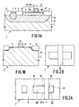
- FIG. 1A,B to 6A,B only a field effect transistor having an n -type channel and a vertical npn transistor are shown, the diagrammatic Figures being each time divided into two associated parts A and B, which show various parts of the same common semiconductor body 1.
- the part A relates to the bipolar transistor and the part B relates to the field effect transistor.
- Figures 1A,B show a semiconductor body 1, which comprises, for example, a p -type silicon substrate or substrate region 2 and is provided in a usual manner with one or more n -type surface regions 32 having a suitably chosen doping concentration profile.
- the surface regions 32 may be obtained, for example, by means of ion implantation, while, if desired, also first a part of the doping may be provided in a substrate, after which a p -type epitaxial layer may be grown and then additionally a further doping may be provided through the surface 5 of the semiconductor body 1 in the epitaxial layer not shown.
- the doping concentration profile in p -type surface regions 31 of the substrate 32 may be adapted, for example by implantation in a usual manner to the circuit elements to be formed and the desired electrical properties thereof.
- the semiconductor body 1 may further be provided in a usual manner with a deep contact zone 8, with a p-type channel stopper zone 33 and with a pattern of field insulation 6.
- the latter pattern may be obtained, for example, by local oxidation of the semiconductor body 1.
- the pattern then consists of silicon oxide.
- Other conventional forms of field insulation, such as filled grooves, may also be used.
- the field insulation 6 limits at the surface 5 active regions for the transistors to be formed.
- the semiconductor body 1 may also comprise one or more n -type surface regions 32 (not shown) which are intended to accomodate in a conventional manner one or more field effect transistors having an insulated gate electrode and a p -type channel. In surface regions 32 intended to accomodate field effect transistors, the deep contact zone 8 may be omitted.
- the surface 5 is provided with an insulating layer 34, which is suitable for use as a dielectric layer for the gate electrodes of the field effect transistors.
- the layer 34 is obtained by thermal oxidation of the semiconductor body 1.
- the thickness of the layer 34 may lie, for example, between about 25 and 50 nm.
- a suitable dose is, for example, about 1.1014 boron atoms/cm2.
- the implantation energy is, for example, about 30 keV.
- the base zone 9 occupies a first part 10 (5) of the surface 5.
- a conductive layer of, for example, polycrystalline or amorphous silicon or of titanium, tantalum, molybdenum or tungsten is provided. If a silicon layer is used as conductive layer, this layer can be doped in a usual manner during the deposition or thereafter, for example by means of PH3.
- the thickness of such a silicon layer is, for example, 500 nm.
- the gate electrode 35 From this layer there is formed besides the gate electrode 35 also a pattern 11 of conductive material which is located above the base zone 9 on the first insulating layer 34 already present.
- the pattern 11 defines at least a first part 36 of the edge 36,37 of an opening 12 ⁇ (cf. also Figures 2A,B).
- the remaining part 37 of the edge 36,37 of the opening 12 ⁇ may coincide practically, for example, with a part of the edge of the pattern of field insulation 6.
- the opening 12 ⁇ may also be defined as a whole by the pattern 11.
- the pattern 11 is, for example annular or it has at least a closed geometry, the edge 36 being located around and at a certain distance from the edge of the pattern of field insulation 6 above the base zone 9.
- the pattern 11 also defines the part 38 of the edge 38,39 of a further opening 40 ⁇ , which is located beside the opening 12 ⁇ also above the first surface part 10 (5).
- the remaining part 39 of this edge 38,39 practically coincides with a part of the edge of the pattern of field insulation 6.
- This insulating layer may comprise, for example, silicon nitride or silicon oxide.
- a doping for source and drain zones 41 and 42 of the field effect transistor is locally provided preferably in the surface region 31 (Fig. 3A,B).
- phosphorus may be implanted at a does of about 1.1013/cm2 and an implantation energy of about 60 keV.
- This doping treatment serves to provide comparatively weakly doped parts 53 of the source zone 41 and the drain zone 42.
- the part of the surface 5 intended for the source zone 41 may also be screened by means of a masking layer (not shown) so that only the drain zone 42 has a comparatively weakly doped part 53 (42).
- an insulating layer of, for example, silicon oxide having a thickness of about 300 nm is deposited on the whole surface of the semiconductor body 1.
- This insulating layer is removed again in a usual manner by anisotropic etching, edge portions 43 being left along the upright edges of the gate electrode 35 and the upright edges 36 and 38 of the pattern 11.
- edge portions of this insulating layer will be maintained also along these edges. Such edge portions are not shown in the Figures for the sake of simplicity.
- openings 12 and 40 of reduced size are obtained inter alia at the area of the openings 12 ⁇ and 40 ⁇ .
- a masking layer 44 is provided on the structure obtained and this masking layer may consist, for example, of photoresist and covers the opening 40.
- a dopant is locally implanted for the source and drain zones 41 and 42 or at least for highly doped surface parts of these zones 41 and 42.
- a dopant for the emitter zone 14 (the second electrode zone) of the bipolar transistor is implanted.
- a dopant for a shallow collector contact zone 15 may be provided.
- arsenic ions are implanted at a dose of about 5.1015/cm2 and an implantation energy of about 40 keV. After this treatment, the layer 44 is removed.
- a doping treatment can be carried out, in which a dopant is provided in the opening 40.
- a dopant for example, BF2 ion may be used to implant boron.
- the dose may be about 3.1015/cm2 and the implantation energy is, for example, about 65 keV.
- This dopant serves to provide a more highly doped base contact zone 46 (9).
- a dopant for source and drain zones of field effect transistors having a p -type channel may also be provided in the semiconductor body 1.
- the layer 45 is removed.
- the pattern 11 provided with edge portions 43 is used as a doping mask, the pattern 11 now defining the edge of the doping opening 40 facing the second electrode zone 14.
- a subsequent treatment consists in providing an insulating layer 16 ( Figures 5A,B).
- silicon oxide is deposited in a thickness of about 500 nm.
- the thickness of the layer 16 is not smaller than 100 to 150 nm.
- the insulating layer 16 constitutes the second insulating layer of the method according to the invention.
- an annealing treatment may be carried out during about one hour at about 925°C. Due to this treatment, where required, the dopants provided are activated.
- a masking layer 48 is provided on the insulating layer 16 and this masking layer may consist, for example, of photoresist, while second openings 49 and 50 are provided in this masking layer.
- this second opening 50 is positioned so that the edge of the first opening 12 derived from the edge 36 of the pattern 11, that is to say the part of the first opening 12 bounded by the edge portion 43, is located at least in part within the second opening 50.
- the semiconductor body 1 is subjected to anisotropic etching treatment, in which openings are obtained in the second insulating layer 16, while, where required, the parts of the first insulating layer 34 located within the openings 49 and 50 are also removed.
- the opening 49 located above the gate electrode 35 is indicated only diagrammatically. In practical embodiments, this opening 49 will mostly be located not above the channel region of the transistor, but outside the cross-section shown beside the transistor and above the field insulation 6.
- edge portions 17 (16) of the second insulating layer 16 are left along the edge of the first opening 12.
- the etching is already continued for such a long time that the parts of the first insulating layer 34 located in these openings 12 and 40 are also removed.
- the doping treatments subsequent to this etching treatment and described already hereinbefore in this case may be carried out with an adapted implantation energy.
- the masking layer 48 can be removed and a conductive layer of a suitable material, such as aluminium, can be provided ( Figures 6A,B).
- a conductive layer of a suitable material such as aluminium
- the conductive layer 22 for connection of the emitter zone 14 is located on a second surface part 23 (5) of the emitter zone 14, which second surface part 23 (5) extends at least at the area at which the edge of the first opening 12 derived from the edge 36 is located within the second opening 50, practically to that edge of the first opening.
- the surface part 23 (5) of the emitter zone 14 has at least at this area practically the same size as the doping opening 12.
- the contact opening for the emitter zone 14 is derived from the doping opening 12 without taking into account the usual alignment tolerance.
- the use of the method according to the invention renders it possible to utilize very small second electrode or emitter zones, which are separated from the first electrode or base zone 9 by a pn junction 24 located at a comparatively small depth.
- the edge portions 17 (16) provided prevent that this pn junction 24 located at a small depth is shortcircuited at the surface 5 by the conductive layer 22.
- This embodiment is a preferred embodiment, in which the second surface region 32 is of the second conductivity type, the first electrode zone 9 is of the first conductivity type and is situated in the second surface region 32 and the first doping treatment is carried out so that the second electrode zone 14 of the second conductivity type is separated by the first electrode zone 9 of the first conductivity type from the part of the second surface region 32 of the second conductivity type adjoining the first electrode zone 9.
- the resulting further circuit element 14,9,32 is a vertically constructed bipolar transistor.
- the second electrode zone 14 may also be one of the main electrode zones of a laterally constructed bipolar transistor, the first electrode zone constituting the control electrode zone (the base zone) of this transistor.
- the first electrode zone may be a part of an epitaxial layer which, if required, may be isolated from the adjoining part of the semiconductor body.
- the further circuit element may also be a diode having an anode zone and a cathode zone or a pn junction field effect transistor, the second electrode zone the constituting, for example, a gate electrode.
- the first insulating layer 34 located below the pattern 11 of conductive material has practically the same thickness as and is obtained simultaneously with the gate dielectric 34, which separates the gate electrode 35 of the field effect transistor 41,35,42 from the first surface region 31.
- the thickness of this insulating layer 34 lies, for example, between about 20 and 50 nm.
- a pattern of refractory conductive material is used as the conductive pattern 11.
- the pattern 11 is formed from one or more materials chosen from the group comprising titanium, tantalum, tungsten, molybdenum, semiconductor material and silicides of these materials.
- the pattern 11 of conductive material in the second opening 50 in the second insulating layer 16 is directly conductively connected to the conductive layer 22.
- an insulating layer of, for example, silicon nitride or silicon oxide is used on the conductive pattern 11, as suggested above in a modification, and if this nitride or oxide layer in the opening 50 is not removed, the pattern 11 and the conductive layer 22 are isolated from each other.
- the conductive pattern 11 can be provided with a conductive connection at a suitably chosen area (not shown) through a further opening in the insulating layer 16, in which the nitride or oxide layer is removed indeed.
- the conductive pattern 11 may be connected in this manner to the conductive layer 21.
- semiconductor materials other than silicon such as germanium and A III B V compounds, may be used.
- the conductivity types described may be inverted and other usual dopants may be employed.
- insulating material for example, oxynitride is also suitable. if for the gate electrode and the pattern use is made of semiconductor material, this may optionally be n - or p -doped, while, if required, it may moreover be converted entirely or in part into a suitable silicide.
- several semiconductor devices may be formed simultaneously in a semiconductor wafer, which is then subdivided into separate semiconductor bodies 1. The semiconductor devices may then be finished in a usual manner in a conventional envelope.
Landscapes
- Electrodes Of Semiconductors (AREA)
- Bipolar Transistors (AREA)
- Metal-Oxide And Bipolar Metal-Oxide Semiconductor Integrated Circuits (AREA)
Claims (5)
- Verfahren zur Herstellung einer integrierten Schaltung mit einem Halbleiterkörper (1) mit einer Oberfläche (5), an die ein erstes und ein zweites Oberflächengebiet (31, 32) grenzen, wobei das erste Oberflächengebiet (31) von einem ersten Leitungstyp ist und für mindestens einen Feldeffekttransistor mit isolierter Gate-Elektrode (35) und mit einer Source-Zone (41) sowie Drain-Zone (42) vom zweiten Leitungstyp bestimmt ist, und wobei das zweite Oberflächengebiet (32) für mindestens ein weiteres Schaltungselement bestimmt ist, das eine an die Oberfläche grenzende erste Elektrodenzone (9) aufweist, die einen ersten Oberflächenteil (10 (5)) der Oberfläche belegt, sowie eine in dem ersten Oberflächenteil (10 (5)) an die Oberfläche grenzende zweite Elektrodenzone (14), die einen zu dem der ersten Elektrodenzone (9) entgegengesetzten Leitungstyp hat, wobei gleichzeitig mit der Gate-Elektrode (35) des Feldeffekttransistors über wenigstens einem Teil der ersten Elektrodenzone (9) ein Muster aus leitendem Material (11) auf einer vorhandenen ersten isolierenden Schicht (34) angebracht wird, wobei dieses Muster mindestens einen ersten Teil (36) des Randes einer bei einer ersten Dotierungsbehandlung zu verwendenden ersten Öffnung (12') zum Anbringen von Dotierung für die zweite Elektrodenzone (14) bestimmt, wobei ein in der ersten Öffnung (12') liegender Teil der ersten Isolierschicht (34) entfernt wird, und wobei nach der ersten Dotierungsbehandlung, wobei gleichzeitig Dotierung für die zweite Elektrodenzone (14) und für die Source- (41) und die Drain-Zone (42) des Feldeffekttransistors angebracht wird, über das Muster (11) und in der ersten Öffnung (12) eine zweite Schicht aus isolierendem Material (16) angebracht wird, wobei die zweite Isolierschicht (16) unter Anwendung einer mit zweiten Öffnungen (49, 50) versehenen maskierenden Schicht (48) örtlich entfernt wird und eine leitende Schicht (22) zum elektrischen Anschluß der zweiten Elektrodenzone (14) angebracht wird, die auf einem zweiten Oberflächenteil (23 (5)) der zweiten Elektrodenzone (14) liegt, dadurch gekennzeichnet, daß beim Entfernen der zweiten Schicht (16) eine zweite Öffnung (50) derart über der zweiten Elektrodenzone (14) liegt, daß der erste Teil (36) des Randes der ersten Öffnung (12) wenigstens teilweise innerhalb der zweiten Öffnung (50) liegt, daß diese örtliche Entfernung der zweiten Schicht (16) in einem anisotropen Ätzverfahren derart durchgeführt wird, daß in der ersten Öffnung (12) ein längs des innerhalb der zweiten Öffnung (50) liegenden Teils des Randes (36) des Musters (11) liegender Randteil 17(16) der zweiten isolierenden Schicht (16) zurückbleibt, wonach die leitende Schicht (22) derart angebracht wird, daß der zweite Oberflächenteil (23 (5)) an der Stelle, wo der Rand der ersten Öffnung (12) innerhalb der zweiten Öffnung (50) liegt, sich nahezu bis an diesen Rand erstreckt.
- Verfahren nach Anspruch 1, dadurch gekennzeichnet, daß das zweite Oberflächengebiet (32) vom zweiten Leitungstyp ist und daß die erste Elektrodenzone (9) vom ersten Leitungstyp ist und in dem zweiten Oberflächengebiet (32) liegt, und wobei die erste Dotierungsbehandlung derart durchgeführt wird, daß die zweite Elektrodenzone (14) vom zweiten Leitungstyp durch die erste Elektrodenzone (9) vom ersten Leitungstyp von dem an die erste Elektrodenzone (9) grenzenden Teil des zweiten Oberflächengebietes (32) vom zweiten Leitungstyp getrennt ist.
- Verfahren nach Anspruch 1 oder 2, dadurch gekennzeichnet, daß gleichzeitig mit der ersten isolierenden Schicht (34) eine weitere isolierende Schicht (43) angebracht wird, die dazu bestimmt ist, die Gate-Elektrode (35) des Feldeffekttransistors vom ersten Oberflächengebiet (31) zu trennen.
- Verfahren nach Anspruch 1, 2 oder 3, dadurch gekennzeichnet, daß das leitende Muster ein Muster aus hochschmelzendem Material ist.
- Verfahren nach Anspruch 1, 2 oder 3, dadurch gekennzeichnet, daß als leitendes Muster (11) ein Muster aus einem oder mehreren Materialien aus der Gruppe Titan, Tantal, Molybdän, Wolfram, Halbleitermaterial und Siliciden dieser Materialien verwendet wird.
Applications Claiming Priority (2)
| Application Number | Priority Date | Filing Date | Title |
|---|---|---|---|
| NL8600770 | 1986-03-26 | ||
| NL8600770A NL8600770A (nl) | 1986-03-26 | 1986-03-26 | Werkwijze voor het vervaardigen van een halfgeleiderinrichting. |
Publications (2)
| Publication Number | Publication Date |
|---|---|
| EP0243988A1 EP0243988A1 (de) | 1987-11-04 |
| EP0243988B1 true EP0243988B1 (de) | 1992-06-17 |
Family
ID=19847772
Family Applications (1)
| Application Number | Title | Priority Date | Filing Date |
|---|---|---|---|
| EP87200372A Expired EP0243988B1 (de) | 1986-03-26 | 1987-03-02 | Verfahren zur Herstellung einer Halbleiteranordnung |
Country Status (6)
| Country | Link |
|---|---|
| US (1) | US4859630A (de) |
| EP (1) | EP0243988B1 (de) |
| JP (1) | JPS62242354A (de) |
| CA (1) | CA1298000C (de) |
| DE (1) | DE3779802T2 (de) |
| NL (1) | NL8600770A (de) |
Families Citing this family (15)
| Publication number | Priority date | Publication date | Assignee | Title |
|---|---|---|---|---|
| SE461428B (sv) * | 1988-06-16 | 1990-02-12 | Ericsson Telefon Ab L M | Foerfarande foer att paa ett underlag av halvledarmaterial framstaella en bipolaer transistor eller en bipolaer transistor och en faelteffekttransistor eller en bipolaer transistor och en faelteffekttransistor med en komplementaer faelteffekttransistor och anordningar framstaellda enligt foerfarandena |
| JPH02291150A (ja) * | 1989-04-28 | 1990-11-30 | Hitachi Ltd | 半導体装置 |
| US5171702A (en) * | 1989-07-21 | 1992-12-15 | Texas Instruments Incorporated | Method for forming a thick base oxide in a BiCMOS process |
| US5268314A (en) * | 1990-01-16 | 1993-12-07 | Philips Electronics North America Corp. | Method of forming a self-aligned bipolar transistor |
| KR940001402B1 (ko) * | 1991-04-10 | 1994-02-21 | 삼성전자 주식회사 | 골드구조를 가지는 반도체소자의 제조방법 |
| GB9219268D0 (en) * | 1992-09-11 | 1992-10-28 | Inmos Ltd | Semiconductor device incorporating a contact and manufacture thereof |
| US5416031A (en) * | 1992-09-30 | 1995-05-16 | Sony Corporation | Method of producing Bi-CMOS transistors |
| US5459083A (en) * | 1993-03-01 | 1995-10-17 | Motorola, Inc. | Method for making BIMOS device having a bipolar transistor and a MOS triggering transistor |
| US5619072A (en) * | 1995-02-09 | 1997-04-08 | Advanced Micro Devices, Inc. | High density multi-level metallization and interconnection structure |
| US6281562B1 (en) | 1995-07-27 | 2001-08-28 | Matsushita Electric Industrial Co., Ltd. | Semiconductor device which reduces the minimum distance requirements between active areas |
| US6124189A (en) * | 1997-03-14 | 2000-09-26 | Kabushiki Kaisha Toshiba | Metallization structure and method for a semiconductor device |
| KR100290903B1 (ko) * | 1998-02-25 | 2001-06-01 | 김영환 | 반도체소자 및 이의 제조방법 |
| KR100275962B1 (ko) | 1998-12-30 | 2001-02-01 | 김영환 | 반도체장치 및 그의 제조방법_ |
| US20010043449A1 (en) | 2000-05-15 | 2001-11-22 | Nec Corporation | ESD protection apparatus and method for fabricating the same |
| US7629210B2 (en) | 2000-05-15 | 2009-12-08 | Nec Corporation | Method for fabricating an ESD protection apparatus for discharging electric charge in a depth direction |
Family Cites Families (7)
| Publication number | Priority date | Publication date | Assignee | Title |
|---|---|---|---|---|
| AU499808B1 (en) * | 1978-05-18 | 1979-05-03 | Ypsilantis, John | Alphanumeric display |
| JPS567463A (en) * | 1979-06-29 | 1981-01-26 | Hitachi Ltd | Semiconductor device and its manufacture |
| US4346512A (en) * | 1980-05-05 | 1982-08-31 | Raytheon Company | Integrated circuit manufacturing method |
| US4356623A (en) * | 1980-09-15 | 1982-11-02 | Texas Instruments Incorporated | Fabrication of submicron semiconductor devices |
| JPS5775453A (en) * | 1980-10-29 | 1982-05-12 | Fujitsu Ltd | Semiconductor device and manufacture thereof |
| DE3205022A1 (de) * | 1981-02-14 | 1982-09-16 | Mitsubishi Denki K.K., Tokyo | Verfahren zum herstellen einer integrierten halbleiterschaltung |
| US4641420A (en) * | 1984-08-30 | 1987-02-10 | At&T Bell Laboratories | Metalization process for headless contact using deposited smoothing material |
-
1986
- 1986-03-26 NL NL8600770A patent/NL8600770A/nl not_active Application Discontinuation
-
1987
- 1987-03-02 DE DE8787200372T patent/DE3779802T2/de not_active Expired - Fee Related
- 1987-03-02 EP EP87200372A patent/EP0243988B1/de not_active Expired
- 1987-03-13 US US07/025,554 patent/US4859630A/en not_active Expired - Lifetime
- 1987-03-18 CA CA000532338A patent/CA1298000C/en not_active Expired - Lifetime
- 1987-03-26 JP JP62070515A patent/JPS62242354A/ja active Granted
Also Published As
| Publication number | Publication date |
|---|---|
| US4859630A (en) | 1989-08-22 |
| EP0243988A1 (de) | 1987-11-04 |
| JPS62242354A (ja) | 1987-10-22 |
| DE3779802D1 (de) | 1992-07-23 |
| CA1298000C (en) | 1992-03-24 |
| NL8600770A (nl) | 1987-10-16 |
| JPH0529147B2 (de) | 1993-04-28 |
| DE3779802T2 (de) | 1993-01-14 |
Similar Documents
| Publication | Publication Date | Title |
|---|---|---|
| US5006476A (en) | Transistor manufacturing process using three-step base doping | |
| EP0265489B1 (de) | Verfahren zur herstellung von halbleiterbauelementen | |
| KR0163402B1 (ko) | 전기적 활성 트렌치 사용 병합 바이폴라/cmos 기술을 사용하는 반도체 구조물 및 그 제조 방법 | |
| US4884117A (en) | Circuit containing integrated bipolar and complementary MOS transistors on a common substrate | |
| US4249968A (en) | Method of manufacturing a metal-insulator-semiconductor utilizing a multiple stage deposition of polycrystalline layers | |
| US6191457B1 (en) | Integrated circuit structure having a bipolar transistor with a thick base oxide and a field effect transistor with a thin gate oxide | |
| EP0243988B1 (de) | Verfahren zur Herstellung einer Halbleiteranordnung | |
| EP0083816B1 (de) | Halbleiteranordnung mit einem Verbindungsmuster | |
| US5198378A (en) | Process of fabricating elevated source/drain transistor | |
| US4745083A (en) | Method of making a fast IGFET | |
| US5882966A (en) | BiDMOS semiconductor device and method of fabricating the same | |
| EP0369336A2 (de) | Prozess zur Herstellung von Bipolar- und CMOS-Transistoren auf einem gemeinsamen Substrat | |
| EP1000439B1 (de) | Verfahren zur herstellung von seitlich dielektrisch isolierten halbleiterbauelementen | |
| JPH06104446A (ja) | 半導体装置 | |
| US5547903A (en) | Method of elimination of junction punchthrough leakage via buried sidewall isolation | |
| US5057455A (en) | Formation of integrated circuit electrodes | |
| EP0242893B1 (de) | Verfahren zur Herstellung einer Halbleiteranordnung | |
| US5571753A (en) | Method for forming a wiring conductor in semiconductor device | |
| US6774455B2 (en) | Semiconductor device with a collector contact in a depressed well-region | |
| US4762804A (en) | Method of manufacturing a bipolar transistor having emitter series resistors | |
| JP2718257B2 (ja) | 集積回路における埋込み層容量の減少 | |
| JP3247106B2 (ja) | 集積回路の製法と集積回路構造 | |
| JPH10289961A (ja) | 半導体装置の製造方法 | |
| JP2003297845A (ja) | 半導体装置およびその製造方法 | |
| KR960005048B1 (ko) | 마스크 롬의 제조방법 |
Legal Events
| Date | Code | Title | Description |
|---|---|---|---|
| PUAI | Public reference made under article 153(3) epc to a published international application that has entered the european phase |
Free format text: ORIGINAL CODE: 0009012 |
|
| AK | Designated contracting states |
Kind code of ref document: A1 Designated state(s): DE FR GB IT NL |
|
| 17P | Request for examination filed |
Effective date: 19880418 |
|
| 17Q | First examination report despatched |
Effective date: 19900730 |
|
| GRAA | (expected) grant |
Free format text: ORIGINAL CODE: 0009210 |
|
| AK | Designated contracting states |
Kind code of ref document: B1 Designated state(s): DE FR GB IT NL |
|
| PG25 | Lapsed in a contracting state [announced via postgrant information from national office to epo] |
Ref country code: NL Effective date: 19920617 |
|
| REF | Corresponds to: |
Ref document number: 3779802 Country of ref document: DE Date of ref document: 19920723 |
|
| ITF | It: translation for a ep patent filed | ||
| ET | Fr: translation filed | ||
| NLV1 | Nl: lapsed or annulled due to failure to fulfill the requirements of art. 29p and 29m of the patents act | ||
| PLBE | No opposition filed within time limit |
Free format text: ORIGINAL CODE: 0009261 |
|
| STAA | Information on the status of an ep patent application or granted ep patent |
Free format text: STATUS: NO OPPOSITION FILED WITHIN TIME LIMIT |
|
| 26N | No opposition filed | ||
| ITTA | It: last paid annual fee | ||
| ITPR | It: changes in ownership of a european patent |
Owner name: CAMBIO RAGIONE SOCIALE;PHILIPS ELECTRONICS N.V. |
|
| REG | Reference to a national code |
Ref country code: FR Ref legal event code: CD |
|
| PGFP | Annual fee paid to national office [announced via postgrant information from national office to epo] |
Ref country code: DE Payment date: 19970523 Year of fee payment: 11 |
|
| PGFP | Annual fee paid to national office [announced via postgrant information from national office to epo] |
Ref country code: GB Payment date: 19980302 Year of fee payment: 12 |
|
| PGFP | Annual fee paid to national office [announced via postgrant information from national office to epo] |
Ref country code: FR Payment date: 19980324 Year of fee payment: 12 |
|
| REG | Reference to a national code |
Ref country code: FR Ref legal event code: CD |
|
| PG25 | Lapsed in a contracting state [announced via postgrant information from national office to epo] |
Ref country code: DE Free format text: LAPSE BECAUSE OF NON-PAYMENT OF DUE FEES Effective date: 19981201 |
|
| PG25 | Lapsed in a contracting state [announced via postgrant information from national office to epo] |
Ref country code: GB Free format text: LAPSE BECAUSE OF NON-PAYMENT OF DUE FEES Effective date: 19990302 |
|
| GBPC | Gb: european patent ceased through non-payment of renewal fee |
Effective date: 19990302 |
|
| PG25 | Lapsed in a contracting state [announced via postgrant information from national office to epo] |
Ref country code: FR Free format text: LAPSE BECAUSE OF NON-PAYMENT OF DUE FEES Effective date: 19991130 |
|
| REG | Reference to a national code |
Ref country code: FR Ref legal event code: ST |
|
| PG25 | Lapsed in a contracting state [announced via postgrant information from national office to epo] |
Ref country code: IT Free format text: LAPSE BECAUSE OF NON-PAYMENT OF DUE FEES;WARNING: LAPSES OF ITALIAN PATENTS WITH EFFECTIVE DATE BEFORE 2007 MAY HAVE OCCURRED AT ANY TIME BEFORE 2007. THE CORRECT EFFECTIVE DATE MAY BE DIFFERENT FROM THE ONE RECORDED. Effective date: 20050302 |