EP0243112A2 - Elektrophotographisches lichtempfindliches Element - Google Patents
Elektrophotographisches lichtempfindliches Element Download PDFInfo
- Publication number
- EP0243112A2 EP0243112A2 EP87303395A EP87303395A EP0243112A2 EP 0243112 A2 EP0243112 A2 EP 0243112A2 EP 87303395 A EP87303395 A EP 87303395A EP 87303395 A EP87303395 A EP 87303395A EP 0243112 A2 EP0243112 A2 EP 0243112A2
- Authority
- EP
- European Patent Office
- Prior art keywords
- layer
- photosensitive member
- electrophotographic photosensitive
- amorphous silicon
- member according
- Prior art date
- Legal status (The legal status is an assumption and is not a legal conclusion. Google has not performed a legal analysis and makes no representation as to the accuracy of the status listed.)
- Withdrawn
Links
Images


Classifications
-
- G—PHYSICS
- G03—PHOTOGRAPHY; CINEMATOGRAPHY; ANALOGOUS TECHNIQUES USING WAVES OTHER THAN OPTICAL WAVES; ELECTROGRAPHY; HOLOGRAPHY
- G03G—ELECTROGRAPHY; ELECTROPHOTOGRAPHY; MAGNETOGRAPHY
- G03G5/00—Recording-members for original recording by exposure, e.g. to light, to heat or to electrons; Manufacture thereof; Selection of materials therefor
- G03G5/02—Charge-receiving layers
- G03G5/04—Photoconductive layers; Charge-generation layers or charge-transporting layers; Additives therefor; Binders therefor
- G03G5/08—Photoconductive layers; Charge-generation layers or charge-transporting layers; Additives therefor; Binders therefor characterised by the photoconductive material being inorganic
- G03G5/082—Photoconductive layers; Charge-generation layers or charge-transporting layers; Additives therefor; Binders therefor characterised by the photoconductive material being inorganic and not being incorporated in a bonding material, e.g. vacuum deposited
- G03G5/08214—Silicon-based
- G03G5/0825—Silicon-based comprising five or six silicon-based layers
Definitions
- the present invention relates to an improvement in the structure of an electrophotographic photosensitive member, and more particularly to an electrophotographic photosensitive member for a laser beam printer using a diode laser.
- the present invention relates to an electrophotographic photosensitive member comprising a photoconductive layer made of amorphous silicon containing germanium incorporated thereinto, particularly to an electrophotographic photosensitive member comprising a conductive support and provided thereon in the following order, a barrier layer, a photoconductive layer, and a surface layer.
- Amorphous selenium, a composite of cadmium sulfide (CdS) and an organic binder, an organic photoconductive member etc. has heretofore been used as an electrophotographic photosensitive member.
- a hydrogenated or halogenated amorphous silicon has recently attracted attention as a photoconductive materials for electrophotographic photosensitive member because of developing the preparation technique of high resistive film with high photoconductivity.
- This photoconductive material is believed to be a substantially ideal electrophotographic photosensitive member since it has not only a higher electrophotographic sensitivity than those of the conventional photoconductive materials but also a high hardness and a low toxicity.
- the electrophotographic photosensitive member comprising a photoconductive layer made of amorphous silicon containing germanium, tin, or the like incorporated thereinto has a high sensitivity even at 750 to 820 nm which are oscillation wavelengths of the GaAlAs diode laser.
- some examples of such photosensitive materials are known as electrophotographic photosensitive members for a diode laser beam printer.
- the conventional electrophotographic photosensitive member comprises a conductive support 101 and provided thereon in the following order, a high resistive film layer 102 (barrier layer or charge transport layer), a photoconductive layer 103 (charge generation layer), and a surface layer 104.
- the high resistive film layer 102 (barrier layer or charge transport layer) is made of amorphous silicon containing carbon incorporated thereinto and has a dark resistivity of 10 12 Q.cm or more.
- the photoconductive layer 103 (charge generation layer) is made of amorphous silicon containing germanium incorporated thereinto and has the sensitivity in the long wavelength range.
- the surface layer 104 is made of amorphous silicon containing carbon incorporated thereinto and has an optical gap of 2.3 eV or more. The surface layer 104 is transparent to visible light and infrared light.
- the photoconductive layer 103 disadvantageously has a lowered resistance because of incorporation of germanium thereinto and hence is poor in the charge acceptance.
- the charge acceptance is supplemented by additional provision of the high resistive film layer 102 and the high resistive surface layer 104, each made of amorphous silicon containing carbon incorporated thereinto, above and under the photoconductive layer 103, thereby improving electrophotographic characteristics such as dark decay and residual potential etc..
- an electrophotographic photosensitive member having the high sensitivity for the long wavelength light is provided.
- the above conventional electrophotographic photosensitive member is thought to be one of those satisfying requirements of a photosensitive member having a high sensitivity for a long wavelength light, but is yet insufficient in many aspects.
- the sensitivity peak of the electrophotographic photosensitive member is located at 700 nm, which is largely deviated from the oscillation wavelengths of the GaAlAs diode laser.
- the sensitivity peak position is adjusted to approach to the oscillation wavelengths of the GaAlAs diode laser by increasing the amount of germanium, the maximum value of the sensitivity is disadvantageously decreased.
- a model band diagram as shown in Fig. 9 is prepared on the assumption that optical gap of respective amorphous silicon layers are pseudo-band gaps (numerals in Fig. 9 correspond to those in Fig. 8).
- the optical gap of the photoconductive layer 103 sensitive to a GaAlAs diode laser of 750 to 820 nm is thought to be 1.5 eV, while that of the surface layer 104 is 2.3 eV or more, thus providing a large energy difference.
- the interface between the photoconductive layer 103 and the surface layer 104 is a place where the layer of combination of silicon and germanium having substantially the same covalent bond radii is in contact with the layer of combination of silicon and carbon having largely different bond radii. In such a place, the localized state (interfacial state) density is high.
- the photoconductive layer 103 made of amorphous silicon containing germanium incorporated thereinto has such an additional problem that it can take charge of only a weak electric fields among the electric fields which have been applied to the whole electrophotographic photosensitive member because of its resistance lower than those of the other layers, which leads to an increase in recombination efficiency of hole and electron through the above-mentioned process, thereby causing lowering in the sensitivity.
- an electrophotographic photosensitive member comprising a conductive support and provided thereon in the following order, a barrier layer, a charge transport layer, and a charge generation layer.
- the charge transport layer is made of amorphous silicon or amorphous silicon containing boron incorporated thereinto.
- the charge generation layer is made of amorphous silicon containing germanium incorporated thereinto.
- the surface protection layer is made of amorphous silicon layer or amorphous silicon layer containing boron incorporated thereinto and provided thereon amorphous silicon carbide layer containing carbon incorporated thereinto.
- the latter electrophotographic photosensitive member has in the electrophotographic sensitivity characteristics for a long wavelength light, however such an electrophotographic sensitivity characteristic is yet insufficient for a longer wavelength light in various aspects.
- the object of the present invention is to overcome at least partly the defects mentioned above and in particular to provide an electrophotographic photosensitive member which has an improved electrophotographic sensitivity for longer wavelength light.
- the invention is set out in claim 1.
- an electrophotographic photosensitive member comprising a surface layer made of amorphous silicon having a wide gap energy (more specifically amorphous silicon containing carbon incorporated thereinto), a photoconductive layer provided thereunder and having a sensitivity for a longer wavelength light, and a barrier layer provided thereunder.
- the present invention can also provide an electrophotographic photosensitive member wherein the energy difference between the surface layer and the photoconductive layer can be reduced, and wherein the interfacial state density between the surface layer and the photoconductive layer can be reduced. Likewise, the energy difference between the photoconductive layer and barrier layer can be reduced, and the interfacial state density between the photoconductive layer and barrier layer can be reduced.
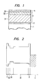
- the electrophotographic photosensitive member comprises a conductive support or a substrate 1 and provided thereon in the following order, a barrier layer 2, a photoconductive layer 3 and a surface layer 4.
- the photoconductive layer 3 has a triple-layer composite structure comprised of an upper layer 33 made of amorphous silicon containing germanium and carbon (for example a-SiGeC:H) incorporated therein on the side of the surface layer 4, a middle layer 32 (charge generation layer) made of amorphous silicon containing germanium (for example a-SiGe:H) incorporated therein, and a lower layer 31 (charge transport layer) made of amorphous silicon (for example a-SiC:H).
- a triple-layer composite structure comprised of an upper layer 33 made of amorphous silicon containing germanium and carbon (for example a-SiGeC:H) incorporated therein on the side of the surface layer 4, a middle layer 32 (charge generation layer) made of amorphous silicon containing germanium (for example a-SiGe:H) incorporated therein, and a lower layer 31 (charge transport layer) made of amorphous silicon (for example a-SiC:H).
- the first proposed feature of the present invention consists in the provision a first intermediate layer being formed between the surface layer and the photoconductive layer and being made of amorphous silicon containing germanium and carbon incorporated thereinto, for example, in the provision of the upper layer 33 containing germanium and carbon incorporated thereinto between the surface layer 4 and the middle layer 32 functioned as a change generation layer.
- the provision of the upper layer 33 containing germanium and carbon incorporated thereinto between the surface layer 4 and the middle layer 32 as shown in Fig. 1 contributes to reduction in the large energy difference as well as reduction in the interfacial state as shown in Fig. 2.
- the second proposed feature of the invention consists in the provision of a second intermediate layer being formed between the photoconductive layer and the barrier layer and being made of amorphous silicon, for example, in the provision of the lower layer 31 made of amorphous silicon as a charge transport layer between the middle layer 32 functioned as a charge generation layer and the barrier layer 2.
- the lower layer 31 is provided between the middle layer 32 and the barrier layer 2.
- a longer wavelength light, particularly a GaAlAs diode laser beam, impinging on the photosensitive member is substantially completely absorbed in a region of a thickness of about 1 ⁇ m of the middle layer 32 (charge generation layer).
- the middle layer 32 charge generation layer
- Such a region of the middle layer 32 is formed at the upper portion of the side of the surface layer 4.
- the charge carriers are generated only in this region of the middle layer 32. Therefore, a region of the middle layer 32 and the lower layer 31, which exists at the side of the barrier layer 2 from the above-mentioned region, can serve to transport the carriers and do not require specially the presence of germanium incorporated thereinto.
- an amorphous silicon having a balanced characteristics in respect of carrier mobility and charge acceptance, particularly an amorphous silicon which has been made intrinsic is used as the lower layer 31.
- h is the Planck constant
- v is a frequency of incident light.
- the absorption spectrum is plotted in the coordinate system, with the hv, of the equation as the abscissa, and the , of the equation as the ordinate. Then the straight line portion of the graph appears therein. The straight line portion is shown with the relationship as formula ⁇ (h ⁇ -E g ).
- the intercept value on the abscissa which is Eg of the above formula, is defined as the optical gap.
- the sensitivity of the electrophotographic photosensitive member in the present invention is obtained as follows.
- the electrophotographic photosensitive member is charged by corona discharge so as to attain the surface potential of about 400-500 V.
- the surface potential of the electrophotographic photosensitive member is lowered rapidly as photoelectric current flows thereon.
- the electrophotographic photosensitive member is reduced the surface potential to half after a lapse of time (t; half value period) from the light irradiation starting time.
- the sensivity (S) of the electrophotographic photosensitive member is obtained by following formula.
- I (mW/m z ) is an irradiation light intensity
- t is a half value period of the surface potential
- the barrier layer 2, the photoconductive layer 3, and the surface layer 4 made of respective amorphous silicon compounds are successively laminated on such a conductive support 1 according to plasma CVD, reactive sputtering, reactive vacuum evaporation, ion plating, or the like methods.
- the films for the barrier layer 2, the photoconductive layer 3, and the surface layer 4 may be formed by the plasma CVD method using a mixture of gases selected from among monosilane (SiH 4 ), hydrocarbon, germane (GeH 4 ), diborane (B 2 H 6 ), phosphine (PH 5 ), and hydrogen (H 2 ).
- the films may be formed by the reactive sputtering method using some of the above-mentioned gases and a silicon and/or germanium target. Further, if desired, film forming methods such as reactive vacuum evaporation and ion plating may also be used.
- Examples of the material of the conductive support 1 to be used in the present invention include metallic materials such as aluminum alloys, stainless steel, iron, steel, copper, copper alloys, nickel, nickel alloys, titanium, and titanium alloys; organic or inorganic materials having a thin metal film of aluminum, chromium, or the like provided thereon or having a thin conductive oxide film of indium tin oxide, tin oxide, indium oxide, or the like provided thereon, among which aluminum alloys are preferable and age-hardening type aluminum alloys are particularly preferable.
- metallic materials such as aluminum alloys, stainless steel, iron, steel, copper, copper alloys, nickel, nickel alloys, titanium, and titanium alloys
- organic or inorganic materials having a thin metal film of aluminum, chromium, or the like provided thereon or having a thin conductive oxide film of indium tin oxide, tin oxide, indium oxide, or the like provided thereon, among which aluminum alloys are preferable and age-hardening type aluminum alloys are particularly preferable.
- the conductive support or the substrate 1 is used in the form of a plate or a drum having a thickness of 1 to 20 mm, or a thin belt having a thickness of 0.1 to 1 mm.
- every layer (the barrier layer 2, the photoconductive layer 3 and the surface layer 4) of the photoconductive layer 3 contains 5 to 40 atomic %, preferably 10 to 20 atomic %, of hydrogen and/or a halogen.
- the halogen is preferably fluorine.
- the barrier layer 2 be made of hydrogenated or halogenated amorphous silicon or hydrogenated or halogenated amorphous silicon containing at least one element selected from among carbon, oxygen, and nitrogen. Further, 1 to 1,000 ppm of an element of group III of the periodic table, such as boron, aluminum, or gallium, is preferably added to such amorphous silicon to control valence electrons for obtaining a p-type semiconductor. A p-type semiconductor prepared by incorporating carbon and boron into such amorphous silicon is particularly preferable.
- the barrier layer 2 have an optical gap of 1.8 to 2.5 eV.
- amorphous silicon of the lower layer 31 of the photoconductive layer 3 be made of an element of group III of the periodic table, such as boron, aluminum, or gallium, particularly boron, be preferably added to such amorphous silicon to make the same intrinsic.
- the lower layer 31 have an intermediate optical gap value between those of the barrier layer 2 and the middle layer 32.
- amorphous silicon containing germanium incorporated therein of the middle layer 32 have the optical gap of 1.4 to 1.6 eV so as to adapt to the oscillation wavelengths of 750-800 nm of the diode laser, which is narrower than than that of the common amorphous silicon. From the composition aspect, the above optical gap of the middle layer 32 is obtained from 20-60 atomic % of germanium against the total amount of silicon and germanium.
- amorphous silicon containing germanium and carbon incorporated therein of the upper layer 33 have the optical gap of 1.2 to 3.0 eV through the various combination of the amount of germanium and silicon.
- the upper layer 32 have an intermediate optical gap value between those of the middle layer 32 and the surface layer 4.
- the optical gap of the upper layer 33 be made to lengthen gradually (continuously or in steps) in passing from the side of the middle layer 32 to the side of the surface layer 4.
- the amount of germanium is made to reduce gradually or the amount of carbon is made to increase gradually.
- the thickness of the upper layer 33 be in a range of 0.005 to 1 pm preferably in a range of 0.01 to 0.5 ⁇ m.
- the surface layer 4 has an optical gap of 1.8 eV or more, which is a broader value than that of the common amorphous silicon.
- amorphous silicon containing carbon incorporated thereinto is suitable so as obtain the range of the optical gap of 2.3 to 3.0 eV from the aspects of charge acceptance, resistance to environment, mechanical strength, resistance to printing, and thermal resistance.
- amorphous silicon containing carbon incorporated thereinto having the range of the optical gap of 2.3 to 3.0 eV of the surface layer 4 is obtained from carbon of 40-90 atomic % against the total amount of silicon and carbon.
- the surface layer 4 has an optical gap of 2.3 to 3.0 eV
- the middle layer 32 has an optical gap energy of 1.4 to 1.6 eV
- the upper layer 33 has an optical gap between those of the surface layer 4 and the middle layer 32.
- the barrier layer 2 has an optical gap of 1.8 to 2.5 eV
- the lower layer 31 has an optical gap between those of the barrier layer 2 and the middle layer 32.
- a model band diagram as shown in Fig. 2 is prepared on the assumption that optical gap of respective amorphous silicon layers are pseudo-band gaps (numerals in Fig. 2 correspond to those in Fig. 1).
- the electrophotographic photosensitive member according to the present invention leads to realization of a high electrophotographic sensitivity for a long wavelength light, thus enabling excellent printing results to be obtained.
- the provision of an intermediate layer between the surface layer and the photoconductive layer serves to reduce the energy difference and the interfacial state between two layers, thereby effectively improving the sensitivity in the oscillation wavelength of the diode laser.
- the provision of an intermediate layer between the the photoconductive layer and the barrier layer serves to reduce the energy difference and the interfacial state between two layers, thereby effectively improving the sensitivity in the oscillation wavelength of the diode laser.
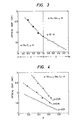
- Fig. 3 shows a relationship between the film composition and the optical gap with respect to an amorphous silicon containing carbon incorporated thereinto (hereinafter represented by "a-Si l - x C x :H”) and to be used as the barrier layer 2 and the surface layer 4, and an amorphous silicon containing germanium incorporated thereinto (hereinafter represented by "a-Si l - x Ge x :H”) and to be used as the middle layer 32.
- a-Si l - x C x :H an amorphous silicon containing carbon incorporated thereinto
- a-Si l - x Ge x :H an amorphous silicon containing germanium incorporated thereinto
- Fig. 4 shows a relationship between the film composition and the optical gap with respect to an amorphous silicon containing germanium and carbon incorporated thereinto (hereinafter represented by "a-Si l - x -yGe x Cy:H”) and to be used as the an upper layer 33.
- the optical gap varies in the range of about 1.2 to 3 eV depending on the amounts of carbon and germanium.
- An electrophotographic photosensitive member having no upper layer was prepared in substantially the same manner as in Example 1 except that the step (4) was dispensed with.
- An electrophotographic photosensitive member was prepared in substantially the same manner as in Example 1 except that the steps (3) and (4) were dispensed with.
- This electrophotographic photosensitive member corresponds to a conventional electrophotographic photosensitive member having no layer made of amorphous silicon containing germanium.
- the spectral sensitivity characteristics of the electrophotographic photosensitive member are shown by the curve B 2 in Fig. 5.
- the photosensitive member of Example 1 of the present invention has a peak sensitivity around 750 nm as compare with those of Comparative Examples 1 and 2.
- the electrophotographic photosensitive member of Example 1 of the present invention has an excellent sensitivity for a longer wavelength light.
- the spectral sensitivity characteristics of the electrophotographic photosensitive member thus obtained are shown by the curve A 2 in Fig. 6.
- the electrophotographic photosensitive member had a superior sensitivity for a longer wavelength light to that of
- Example 2 Substantially the same procedure as in Example 1 except that the composition of-an upper layer was continuously changed from a-Si 0.7 Ge 0.2 C 0.1 :H to a-Si 0.3 C 0.7 :H in substantially the same manner as in Example 2 was repeated to prepared an electrophotographic photosensitive member.
- Example 1 The result of Example 1 is shown by the curve A l in Fig. 6.
- Example 3 The following conclusion can be obtained by the comparison of Example 2 with Example 3 as shown in Fig 6.
- a difference between the electrophotographic photosensitive members of Example 2 and Example 3 is that the former has a region of narrow optical gap (for example, 1.8 to 1.5 eV) while the latter has no such a region. Since charge carrier is generated in a region of narrow optical gap by the irradiation with a long wavelength light, the improvement in the sensitivity for a longer wavelength light is attained principally by reduction in the energy difference and the interfacial state.
- Example 2 Substantially the same procedure as in Example 2 except that CH 4 was used as the carbon source instead of C 2 H 4 in the step (4a) of forming an upper layer was repeated. Also in this method, the composition a-Si l - x -yGe x Cy:H could be continuously changed while the amount of carbon was gradually increased. The other steps were the same as in Example 1.
- An upper layer was formed in substantially the same manner as in Example 4 except that CH 4 was initially introduced as the carbon source gas and gradually replaced with C 2 H 4 , and only C 2 H 4 was finally introduced.
- the other steps were the same as in Example 1.
- Example 2 The result of Example 2 is shown in the curve A 2 in Fig. 7.
- CH 4 is used as the carbon source gas
- Combined use of CH 4 with C 2 H 4 can change the composition in a wider range and, therefore, is more effective.
Landscapes
- Chemical & Material Sciences (AREA)
- Inorganic Chemistry (AREA)
- Physics & Mathematics (AREA)
- General Physics & Mathematics (AREA)
- Photoreceptors In Electrophotography (AREA)
Applications Claiming Priority (2)
| Application Number | Priority Date | Filing Date | Title |
|---|---|---|---|
| JP89517/86 | 1986-04-18 | ||
| JP8951786 | 1986-04-18 |
Publications (2)
| Publication Number | Publication Date |
|---|---|
| EP0243112A2 true EP0243112A2 (de) | 1987-10-28 |
| EP0243112A3 EP0243112A3 (de) | 1989-08-30 |
Family
ID=13972989
Family Applications (1)
| Application Number | Title | Priority Date | Filing Date |
|---|---|---|---|
| EP87303395A Withdrawn EP0243112A3 (de) | 1986-04-18 | 1987-04-16 | Elektrophotographisches lichtempfindliches Element |
Country Status (3)
| Country | Link |
|---|---|
| US (1) | US4791040A (de) |
| EP (1) | EP0243112A3 (de) |
| JP (1) | JPH0670717B2 (de) |
Families Citing this family (1)
| Publication number | Priority date | Publication date | Assignee | Title |
|---|---|---|---|---|
| JPH02181154A (ja) * | 1989-01-04 | 1990-07-13 | Fuji Xerox Co Ltd | 電子写真感光体 |
Family Cites Families (12)
| Publication number | Priority date | Publication date | Assignee | Title |
|---|---|---|---|---|
| US4491626A (en) * | 1982-03-31 | 1985-01-01 | Minolta Camera Kabushiki Kaisha | Photosensitive member |
| JPS58189643A (ja) * | 1982-03-31 | 1983-11-05 | Minolta Camera Co Ltd | 感光体 |
| JPS58192044A (ja) * | 1982-05-06 | 1983-11-09 | Konishiroku Photo Ind Co Ltd | 感光体 |
| JPS5984254A (ja) * | 1982-11-08 | 1984-05-15 | Konishiroku Photo Ind Co Ltd | 感光体 |
| JPS59149371A (ja) * | 1983-02-16 | 1984-08-27 | Hitachi Ltd | 受光面 |
| JPS59190955A (ja) * | 1983-04-11 | 1984-10-29 | ユ−オ−ピ−・インコ−ポレイテツド | アミノ酸ラセミ体の分割 |
| US4513073A (en) * | 1983-08-18 | 1985-04-23 | Minnesota Mining And Manufacturing Company | Layered photoconductive element |
| JPS60104954A (ja) * | 1983-11-11 | 1985-06-10 | Hitachi Koki Co Ltd | 電子写真像形成部材 |
| JPH067270B2 (ja) * | 1983-12-16 | 1994-01-26 | 株式会社日立製作所 | 電子写真用感光体 |
| JPS6126053A (ja) * | 1984-07-16 | 1986-02-05 | Minolta Camera Co Ltd | 電子写真感光体 |
| JPS6129847A (ja) * | 1984-07-20 | 1986-02-10 | Minolta Camera Co Ltd | 電子写真感光体 |
| JPS61221752A (ja) * | 1985-03-12 | 1986-10-02 | Sharp Corp | 電子写真感光体 |
-
1987
- 1987-04-15 JP JP62090773A patent/JPH0670717B2/ja not_active Expired - Lifetime
- 1987-04-16 EP EP87303395A patent/EP0243112A3/de not_active Withdrawn
- 1987-04-20 US US07/041,246 patent/US4791040A/en not_active Expired - Fee Related
Also Published As
| Publication number | Publication date |
|---|---|
| JPS6355557A (ja) | 1988-03-10 |
| JPH0670717B2 (ja) | 1994-09-07 |
| EP0243112A3 (de) | 1989-08-30 |
| US4791040A (en) | 1988-12-13 |
Similar Documents
| Publication | Publication Date | Title |
|---|---|---|
| US4329699A (en) | Semiconductor device and method of manufacturing the same | |
| EP0309000B1 (de) | Amorpher Halbleiter und photovoltaische Vorrichtung aus amorphem Silizium | |
| US4495262A (en) | Photosensitive member for electrophotography comprises inorganic layers | |
| US4109271A (en) | Amorphous silicon-amorphous silicon carbide photovoltaic device | |
| EP0523919B1 (de) | Photovoltische Vorrichtung mit mehreren Übergängen und Herstellungsverfahren | |
| JPH09512665A (ja) | 高水素希釈低温プラズマ沈着によって製造される非晶質珪素ベースの器具の向上せしめられた安定化特性 | |
| EP0317350B1 (de) | Photovoltaisches PIN-Bauelement, Tandem-und Triple-Zellen | |
| Gau et al. | Preparation of amorphous silicon films by chemical vapor deposition from higher silanes SinH2n+ 2 (n≳ 1) | |
| JPS6055347A (ja) | 光導電性要素 | |
| EP0241274B1 (de) | Lichtempfindliches Element | |
| US5741615A (en) | Light receiving member with non-single-crystal silicon layer containing Cr, Fe, Na, Ni and Mg | |
| US4672015A (en) | Electrophotographic member having multilayered amorphous silicon photosensitive member | |
| EP0243112A2 (de) | Elektrophotographisches lichtempfindliches Element | |
| EP0139961B1 (de) | Photorezeptor für die Elektrophotographie | |
| EP0300807A2 (de) | Elektrophotographisches lichtempfindliches Element | |
| US5190838A (en) | Electrophotographic image-forming member with photoconductive layer comprising non-single-crystal silicon carbide | |
| JP3559655B2 (ja) | 電子写真用光受容部材 | |
| US4965164A (en) | Method for producing electrophotographic photoreceptor | |
| JPH0652428B2 (ja) | 光導電体 | |
| US4762761A (en) | Electrophotographic photosensitive member and the method of manufacturing the same comprises micro-crystalline silicon | |
| US4704343A (en) | Electrophotographic photosensitive member containing amorphous silicon and doped microcrystalline silicon layers | |
| JPS62151857A (ja) | 光導電部材 | |
| JP2668407B2 (ja) | 電子写真用像形成部材 | |
| JPH0997919A (ja) | 光導電膜及びその製造方法並びにその膜を用いた光起電力素子 | |
| JP3210935B2 (ja) | 光受容部材 |
Legal Events
| Date | Code | Title | Description |
|---|---|---|---|
| PUAI | Public reference made under article 153(3) epc to a published international application that has entered the european phase |
Free format text: ORIGINAL CODE: 0009012 |
|
| 17P | Request for examination filed |
Effective date: 19870601 |
|
| AK | Designated contracting states |
Kind code of ref document: A2 Designated state(s): DE FR GB IT NL |
|
| PUAL | Search report despatched |
Free format text: ORIGINAL CODE: 0009013 |
|
| AK | Designated contracting states |
Kind code of ref document: A3 Designated state(s): DE FR GB IT NL |
|
| 17Q | First examination report despatched |
Effective date: 19920319 |
|
| STAA | Information on the status of an ep patent application or granted ep patent |
Free format text: STATUS: THE APPLICATION IS DEEMED TO BE WITHDRAWN |
|
| 18D | Application deemed to be withdrawn |
Effective date: 19940426 |
|
| RIN1 | Information on inventor provided before grant (corrected) |
Inventor name: ONUMA, SHIGEHARU Inventor name: TAMAHASHI, KUNIHIRO Inventor name: SHIMAMURA, YASUO Inventor name: CHIGASAKI, MITSUO Inventor name: OHNO, TOSHIYUJI Inventor name: FUJIKURA, MAKOTO |