EP0241692A2 - Dispositif pour éviter la dégradation indésirable pendant le fonctionnement à vide de modules solaires comprenant en particulier des cellules au silicium amorphe - Google Patents
Dispositif pour éviter la dégradation indésirable pendant le fonctionnement à vide de modules solaires comprenant en particulier des cellules au silicium amorphe Download PDFInfo
- Publication number
- EP0241692A2 EP0241692A2 EP87103089A EP87103089A EP0241692A2 EP 0241692 A2 EP0241692 A2 EP 0241692A2 EP 87103089 A EP87103089 A EP 87103089A EP 87103089 A EP87103089 A EP 87103089A EP 0241692 A2 EP0241692 A2 EP 0241692A2
- Authority
- EP
- European Patent Office
- Prior art keywords
- module
- amorphous silicon
- consumer
- solar cells
- degradation during
- Prior art date
- Legal status (The legal status is an assumption and is not a legal conclusion. Google has not performed a legal analysis and makes no representation as to the accuracy of the status listed.)
- Ceased
Links
Images
Classifications
-
- H—ELECTRICITY
- H10—SEMICONDUCTOR DEVICES; ELECTRIC SOLID-STATE DEVICES NOT OTHERWISE PROVIDED FOR
- H10F—INORGANIC SEMICONDUCTOR DEVICES SENSITIVE TO INFRARED RADIATION, LIGHT, ELECTROMAGNETIC RADIATION OF SHORTER WAVELENGTH OR CORPUSCULAR RADIATION
- H10F77/00—Constructional details of devices covered by this subclass
- H10F77/95—Circuit arrangements
- H10F77/953—Circuit arrangements for devices having potential barriers
- H10F77/955—Circuit arrangements for devices having potential barriers for photovoltaic devices
-
- H—ELECTRICITY
- H10—SEMICONDUCTOR DEVICES; ELECTRIC SOLID-STATE DEVICES NOT OTHERWISE PROVIDED FOR
- H10F—INORGANIC SEMICONDUCTOR DEVICES SENSITIVE TO INFRARED RADIATION, LIGHT, ELECTROMAGNETIC RADIATION OF SHORTER WAVELENGTH OR CORPUSCULAR RADIATION
- H10F10/00—Individual photovoltaic cells, e.g. solar cells
- H10F10/10—Individual photovoltaic cells, e.g. solar cells having potential barriers
- H10F10/17—Photovoltaic cells having only PIN junction potential barriers
-
- H—ELECTRICITY
- H10—SEMICONDUCTOR DEVICES; ELECTRIC SOLID-STATE DEVICES NOT OTHERWISE PROVIDED FOR
- H10F—INORGANIC SEMICONDUCTOR DEVICES SENSITIVE TO INFRARED RADIATION, LIGHT, ELECTROMAGNETIC RADIATION OF SHORTER WAVELENGTH OR CORPUSCULAR RADIATION
- H10F19/00—Integrated devices, or assemblies of multiple devices, comprising at least one photovoltaic cell covered by group H10F10/00, e.g. photovoltaic modules
-
- H—ELECTRICITY
- H10—SEMICONDUCTOR DEVICES; ELECTRIC SOLID-STATE DEVICES NOT OTHERWISE PROVIDED FOR
- H10F—INORGANIC SEMICONDUCTOR DEVICES SENSITIVE TO INFRARED RADIATION, LIGHT, ELECTROMAGNETIC RADIATION OF SHORTER WAVELENGTH OR CORPUSCULAR RADIATION
- H10F77/00—Constructional details of devices covered by this subclass
- H10F77/10—Semiconductor bodies
- H10F77/16—Material structures, e.g. crystalline structures, film structures or crystal plane orientations
- H10F77/162—Non-monocrystalline materials, e.g. semiconductor particles embedded in insulating materials
- H10F77/166—Amorphous semiconductors
- H10F77/1662—Amorphous semiconductors including only Group IV materials
-
- Y—GENERAL TAGGING OF NEW TECHNOLOGICAL DEVELOPMENTS; GENERAL TAGGING OF CROSS-SECTIONAL TECHNOLOGIES SPANNING OVER SEVERAL SECTIONS OF THE IPC; TECHNICAL SUBJECTS COVERED BY FORMER USPC CROSS-REFERENCE ART COLLECTIONS [XRACs] AND DIGESTS
- Y02—TECHNOLOGIES OR APPLICATIONS FOR MITIGATION OR ADAPTATION AGAINST CLIMATE CHANGE
- Y02B—CLIMATE CHANGE MITIGATION TECHNOLOGIES RELATED TO BUILDINGS, e.g. HOUSING, HOUSE APPLIANCES OR RELATED END-USER APPLICATIONS
- Y02B10/00—Integration of renewable energy sources in buildings
- Y02B10/10—Photovoltaic [PV]
-
- Y—GENERAL TAGGING OF NEW TECHNOLOGICAL DEVELOPMENTS; GENERAL TAGGING OF CROSS-SECTIONAL TECHNOLOGIES SPANNING OVER SEVERAL SECTIONS OF THE IPC; TECHNICAL SUBJECTS COVERED BY FORMER USPC CROSS-REFERENCE ART COLLECTIONS [XRACs] AND DIGESTS
- Y02—TECHNOLOGIES OR APPLICATIONS FOR MITIGATION OR ADAPTATION AGAINST CLIMATE CHANGE
- Y02E—REDUCTION OF GREENHOUSE GAS [GHG] EMISSIONS, RELATED TO ENERGY GENERATION, TRANSMISSION OR DISTRIBUTION
- Y02E10/00—Energy generation through renewable energy sources
- Y02E10/50—Photovoltaic [PV] energy
- Y02E10/548—Amorphous silicon PV cells
-
- Y—GENERAL TAGGING OF NEW TECHNOLOGICAL DEVELOPMENTS; GENERAL TAGGING OF CROSS-SECTIONAL TECHNOLOGIES SPANNING OVER SEVERAL SECTIONS OF THE IPC; TECHNICAL SUBJECTS COVERED BY FORMER USPC CROSS-REFERENCE ART COLLECTIONS [XRACs] AND DIGESTS
- Y10—TECHNICAL SUBJECTS COVERED BY FORMER USPC
- Y10S—TECHNICAL SUBJECTS COVERED BY FORMER USPC CROSS-REFERENCE ART COLLECTIONS [XRACs] AND DIGESTS
- Y10S136/00—Batteries: thermoelectric and photoelectric
- Y10S136/291—Applications
- Y10S136/293—Circuits
Definitions
- the invention relates to an arrangement for avoiding unwanted degradation during idle operation of solar cells consisting in particular of amorphous silicon, which are interconnected in modules.
- Solar cells can be used particularly advantageously where low maintenance for plants or devices is possible or where other electrical energy sources are not available. The latter applies particularly to the use of small devices for caravans, sailing boats, mountain huts or the like.
- Amorphous silicon solar cells have recently become increasingly important. Compared to crystalline silicon solar cells, they have the advantage of cheaper production because of their thin-film construction. However, the stability of solar cells made of amorphous silicon poses problems, the elimination of which has been the subject of many studies. For example, from a report by M. Moeller et. al. from the conference proceedings of the Materials Research Society Symposium 1985, Vol.
- the measures discussed here also lead to solar cells or modules in which aging occurs significantly less under load, i.e. when the consumer is connected, than when the module is idling. This is particularly the case in modules with efficiencies greater than 5%, which are produced with the cell type glass substrate / tin oxide as the base electrode / p-SiC-i-n as the thin film / metal as the back electrode.
- the degradation of these modules can be very low with a suitable production after an initial aging of a few percent, for example less than 10% after 10 years of operation in sunlight if they are operated continuously under load. Operation under idle conditions, on the other hand, can double the degradation. These idle conditions occur if the module is accidentally not connected to the consumer, or if the consumer is deliberately or unintentionally disconnected from the module despite cable termination, for example in the event of a cable defect. In any case, the effect is a premature, unnoticed decrease in module performance due to the degradation.
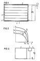
- FIG. 1 shows a module 1, consisting of a plurality of solar cells 2, which are electrically conductively interconnected, are provided with two contact strips 3.
- Contacts 5 and 6 are attached to the frame 4 of the module 1, through which the solar cells 2 generating the electrical current are connected to the consumer.
- a switch 7 with a load resistor R L is now installed, which is opened when the module is separated from the consumer, that is to say is operated in idle mode, and is closed when the consumer is connected , that is, when the module is in operation.
- voltage and current in a suitable form, can be used in such a way that the internal load resistance R L is only switched off when the signal I m / U m (see FIG. 2) exceeds a certain value.
- a simple, inexpensive circuit can be used, which does not significantly affect the cost of the module and has a low power requirement. .
Landscapes
- Photovoltaic Devices (AREA)
- Control Of Electrical Variables (AREA)
Applications Claiming Priority (2)
| Application Number | Priority Date | Filing Date | Title |
|---|---|---|---|
| DE3610083 | 1986-03-25 | ||
| DE3610083 | 1986-03-25 |
Publications (2)
| Publication Number | Publication Date |
|---|---|
| EP0241692A2 true EP0241692A2 (fr) | 1987-10-21 |
| EP0241692A3 EP0241692A3 (fr) | 1989-05-10 |
Family
ID=6297244
Family Applications (1)
| Application Number | Title | Priority Date | Filing Date |
|---|---|---|---|
| EP87103089A Ceased EP0241692A3 (fr) | 1986-03-25 | 1987-03-04 | Dispositif pour éviter la dégradation indésirable pendant le fonctionnement à vide de modules solaires comprenant en particulier des cellules au silicium amorphe |
Country Status (3)
| Country | Link |
|---|---|
| US (1) | US4744835A (fr) |
| EP (1) | EP0241692A3 (fr) |
| JP (1) | JPS62231321A (fr) |
Families Citing this family (2)
| Publication number | Priority date | Publication date | Assignee | Title |
|---|---|---|---|---|
| WO2009145678A1 (fr) * | 2008-05-26 | 2009-12-03 | Volvo Technology Corporation | Module interrupteur pour un réseau d'alimentation électrique et réseau d'alimentation électrique comprenant au moins un module interrupteur |
| WO2010106799A1 (fr) * | 2009-03-18 | 2010-09-23 | 富士電機システムズ株式会社 | Module de cellule solaire |
Family Cites Families (4)
| Publication number | Priority date | Publication date | Assignee | Title |
|---|---|---|---|---|
| US4341607A (en) * | 1980-12-08 | 1982-07-27 | E:F Technology, Inc. | Solar power system requiring no active control device |
| JPS58216476A (ja) * | 1982-06-11 | 1983-12-16 | Hitachi Ltd | 光発電蓄電装置 |
| DE3415828A1 (de) * | 1983-04-30 | 1984-11-29 | Kyocera Corp., Kyoto | Solarzellenanordnung |
| JPS61141184A (ja) * | 1984-12-14 | 1986-06-28 | Hitachi Maxell Ltd | 太陽電池付装置 |
-
1987
- 1987-01-02 US US07/000,160 patent/US4744835A/en not_active Expired - Fee Related
- 1987-03-04 EP EP87103089A patent/EP0241692A3/fr not_active Ceased
- 1987-03-20 JP JP62067699A patent/JPS62231321A/ja active Pending
Also Published As
| Publication number | Publication date |
|---|---|
| JPS62231321A (ja) | 1987-10-09 |
| EP0241692A3 (fr) | 1989-05-10 |
| US4744835A (en) | 1988-05-17 |
Similar Documents
| Publication | Publication Date | Title |
|---|---|---|
| EP1006593B1 (fr) | Module solaire photovoltaique en form de plaque | |
| DE3031907A1 (de) | Solarzelle und solarzellenverbund sowie verfahren zu ihrer herstellung. | |
| EP2139046A1 (fr) | Module photovoltaïque | |
| DE102010060463B4 (de) | Schaltungsanordnung zur Potentialeinstellung eines Photovoltaikgenerators und Photovoltaikanlage | |
| DE1210479B (de) | UEberladungs-Schutzeinrichtung fuer eine wiederaufladbare elektrische Sammler-Batterie | |
| WO2014037382A1 (fr) | Dispositif de connexion électrique non permanente de cellules solaires afin de mesurer des propriétés électriques | |
| DE2646715B2 (de) | Am Handgelenk zu tragendes Instrument | |
| WO2013097964A1 (fr) | Agencement de cellules photovoltaïques à configuration en tandem | |
| EP0198196A2 (fr) | Cellule solaire avec un corps semi-conducteur au silicium amorphe du type p-SiC/i/n | |
| DE3313792A1 (de) | Verfahren zur spannungsanpassung von zellen mit hoher spannung sowie zellenanordnung hierfuer | |
| DE8608204U1 (de) | Aus amorphem Silizium bestehendes Solarzellenmodul | |
| DE19910532B4 (de) | Photovoltaisches Solarmodul in Plattenform | |
| DE3005560A1 (de) | Reihenschaltung von solarzellen | |
| EP4160908B1 (fr) | Module photovoltaïque et ensemble de connexion pour un module photovoltaïque | |
| EP0528326A1 (fr) | Lampe solaire d'avertissement | |
| DE202020003408U1 (de) | Batteriesystem, insbesondere Bipolarbatteriesystem | |
| EP3573110A1 (fr) | Module solaire à surface d'ouverture agrandie | |
| DE102011079505A1 (de) | Solarzellenbaustein und Solarzellenanordnung | |
| EP3858637A1 (fr) | Chemise pour une carte de menu et/ou de boisson doté d'un module de lumière plat, dispositif de maintien pour la chemise, procédé de fabrication de module de lumière | |
| DE10347647A1 (de) | Solarzellenanordnung | |
| DE2924631A1 (de) | Vorrichtung zum betreiben eines elektrischen geraetes, beispielsweise eines elektro-weidezaungeraetes, aus einem solarzellengenerator | |
| DE102012007443A1 (de) | Minuspolerdung | |
| DE1924826A1 (de) | Steuerschaltung | |
| DE102018108104A1 (de) | Photovoltaik-Stromversorgungsvorrichtung, insbesondere vom öffentlichen Stromnetz unabhängige Photovoltaik-Stromversorgungsvorrichtung, und hierfür geeignete Ladeschaltungsanordnung | |
| WO2011029791A1 (fr) | Système d'accumulateurs au lithium destiné en particulier à être utilisé dans un réseau de bord standard à 14 v |
Legal Events
| Date | Code | Title | Description |
|---|---|---|---|
| PUAI | Public reference made under article 153(3) epc to a published international application that has entered the european phase |
Free format text: ORIGINAL CODE: 0009012 |
|
| AK | Designated contracting states |
Kind code of ref document: A2 Designated state(s): DE FR GB |
|
| PUAL | Search report despatched |
Free format text: ORIGINAL CODE: 0009013 |
|
| AK | Designated contracting states |
Kind code of ref document: A3 Designated state(s): DE FR GB |
|
| 17P | Request for examination filed |
Effective date: 19891026 |
|
| 17Q | First examination report despatched |
Effective date: 19910507 |
|
| STAA | Information on the status of an ep patent application or granted ep patent |
Free format text: STATUS: THE APPLICATION HAS BEEN REFUSED |
|
| 18R | Application refused |
Effective date: 19911101 |
|
| RIN1 | Information on inventor provided before grant (corrected) |
Inventor name: WINSTEL, GUENTER, DR.RER.NAT. Inventor name: PLAETTNER, ROLF, DR.PHIL.NAT. |