EP0241077B1 - Kodierungsvorrichtung - Google Patents
Kodierungsvorrichtung Download PDFInfo
- Publication number
- EP0241077B1 EP0241077B1 EP87200562A EP87200562A EP0241077B1 EP 0241077 B1 EP0241077 B1 EP 0241077B1 EP 87200562 A EP87200562 A EP 87200562A EP 87200562 A EP87200562 A EP 87200562A EP 0241077 B1 EP0241077 B1 EP 0241077B1
- Authority
- EP
- European Patent Office
- Prior art keywords
- input
- signal
- output
- filter
- summing circuit
- Prior art date
- Legal status (The legal status is an assumption and is not a legal conclusion. Google has not performed a legal analysis and makes no representation as to the accuracy of the status listed.)
- Expired - Lifetime
Links
Images


Classifications
-
- H—ELECTRICITY
- H03—ELECTRONIC CIRCUITRY
- H03M—CODING; DECODING; CODE CONVERSION IN GENERAL
- H03M1/00—Analogue/digital conversion; Digital/analogue conversion
-
- H—ELECTRICITY
- H03—ELECTRONIC CIRCUITRY
- H03M—CODING; DECODING; CODE CONVERSION IN GENERAL
- H03M3/00—Conversion of analogue values to or from differential modulation
- H03M3/30—Delta-sigma modulation
- H03M3/39—Structural details of delta-sigma modulators, e.g. incremental delta-sigma modulators
- H03M3/436—Structural details of delta-sigma modulators, e.g. incremental delta-sigma modulators characterised by the order of the loop filter, e.g. error feedback type
- H03M3/438—Structural details of delta-sigma modulators, e.g. incremental delta-sigma modulators characterised by the order of the loop filter, e.g. error feedback type the modulator having a higher order loop filter in the feedforward path
- H03M3/44—Structural details of delta-sigma modulators, e.g. incremental delta-sigma modulators characterised by the order of the loop filter, e.g. error feedback type the modulator having a higher order loop filter in the feedforward path with provisions for rendering the modulator inherently stable
- H03M3/442—Structural details of delta-sigma modulators, e.g. incremental delta-sigma modulators characterised by the order of the loop filter, e.g. error feedback type the modulator having a higher order loop filter in the feedforward path with provisions for rendering the modulator inherently stable by restricting the swing within the loop, e.g. gain scaling
- H03M3/444—Structural details of delta-sigma modulators, e.g. incremental delta-sigma modulators characterised by the order of the loop filter, e.g. error feedback type the modulator having a higher order loop filter in the feedforward path with provisions for rendering the modulator inherently stable by restricting the swing within the loop, e.g. gain scaling using non-linear elements, e.g. limiters
-
- H—ELECTRICITY
- H03—ELECTRONIC CIRCUITRY
- H03M—CODING; DECODING; CODE CONVERSION IN GENERAL
- H03M3/00—Conversion of analogue values to or from differential modulation
- H03M3/30—Delta-sigma modulation
- H03M3/39—Structural details of delta-sigma modulators, e.g. incremental delta-sigma modulators
- H03M3/412—Structural details of delta-sigma modulators, e.g. incremental delta-sigma modulators characterised by the number of quantisers and their type and resolution
- H03M3/422—Structural details of delta-sigma modulators, e.g. incremental delta-sigma modulators characterised by the number of quantisers and their type and resolution having one quantiser only
- H03M3/43—Structural details of delta-sigma modulators, e.g. incremental delta-sigma modulators characterised by the number of quantisers and their type and resolution having one quantiser only the quantiser being a single bit one
-
- H—ELECTRICITY
- H03—ELECTRONIC CIRCUITRY
- H03M—CODING; DECODING; CODE CONVERSION IN GENERAL
- H03M3/00—Conversion of analogue values to or from differential modulation
- H03M3/30—Delta-sigma modulation
- H03M3/39—Structural details of delta-sigma modulators, e.g. incremental delta-sigma modulators
- H03M3/436—Structural details of delta-sigma modulators, e.g. incremental delta-sigma modulators characterised by the order of the loop filter, e.g. error feedback type
- H03M3/456—Structural details of delta-sigma modulators, e.g. incremental delta-sigma modulators characterised by the order of the loop filter, e.g. error feedback type the modulator having a first order loop filter in the feedforward path
Definitions
- the invention relates to an encoding device comprising a quantizer for converting an input signal into a one-bit encoded signal, which quantizer comprises an input for receiving the input signal and an output for supplying the one-bit encoded signal, and further comprising error-feedback means for feeding back to the quantizer input a quantization-error signal caused by the quantizer, which error-feedback means comprise an at least third-order filter having an input and an output.
- Such a device is suitable for use in analog-to-digital and digital-to-analog converters.
- analog-to-digital conversion the bandwidth of the analog signal is usually limited to substantially half the sampling frequency by means of an analog low-pass filter, after which sampling and quantization is effected.
- an analog audio signal for example with a frequency of 44.1 kHz, can be sampled and can subsequently be converted into a 16-bit pulse-code modulated signal.
- Such an analog-to-digital conversion imposes very stringent requirements on the analog input filter in view of the required frequency roll-off above the signal band and on the quantizer in view of the accuracy required for 16-bit quantization.
- this 1-bit signal can subsequently by converted into, for example, a 16-bit pulse-code-modulated signal having a lower sampling frequency.
- the decimating filter comprises a digital low-pass filter followed by a down-sampler.
- the low-pass filter is then required to have a steep roll-off above the signal band, which is easier to realize for a digital filter than for an analog filter.
- the 1-bit encoding device may then be a device in which the quantization error produced by the quantizer is substracted from the input signal via a loop filter before this signal is applied to the quantizer. If the transfer function of this loop filter is substantially unity within the signal band and rolls off steeply above this band, this ensures that the quantization noise, corresponding to the quantization errors, in the 1-bit encoded signal within the signal band is attenuated at the expense of an increase in quantization noise outside the signal band.
- a similar encoding device may also be employed in a digital-to-analog converter in which, for example, a 16-bit pulse-code-modulated signal with a sampling frequency of 44.1 kHz is first converted into a 28-bit encoded signal with a sampling frequency of 176.4 kHz by means of an interpolating filter and is subsequently re-converted into a 1-bit signal by means of encoding device, the quantization error being substrated from the input signal via a loop filter. Again this results in a reduction of the quantization noise in the 1-bit signal within the signal band at the expense of an increase of this noise above the signal band. Subsequently, the 1-bit output signal is applied to the actual 1-bit digital-to-analog converter, which can be realized in a comparatively simple manner.
- An encoding device of the type defined in the opening paragraph is known from German Patent Specification 3,021,012, in which the device is employed in order to reduce the quantization noise in a digital-to-analog converter in a way similar to that described above.
- Said Patent Specification also states that the reduction of quantization-noise within the signal band increases as the order of the loop filter is higher.
- Such loop filters provide a satisfactory reduction of quantization noise within the signal band, but this known encoding device has the disadvantage that it exhibits instabilities for loop filters of orders higher than the second order.
- the value of the constant a depends on the filter order.
- the input signal of the encoding device may be both a discrete-time amplitude-continuous signal and a digital signal.
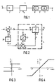
- Fig. 1 shows the basic diagram of an analog-to-digital converter 1 in which an encoding device in accordance with the invention may be used.
- the converter 1 comprises an analog input filter 2 having an input 3 for receiving an analog input signal.
- This input signal is, for example, an audio signal.
- the output signal of the filter 2 is applied to a 1-bit encoding device 4 which converts this signal into a 1-bit encoded signal having a sampling frequency f s which is comparatively high relative to the maximum signal frequency.
- this sampling frequency is, for example, 5.6 MHz.
- the input filter 2 may exhibit a comparatively low-order roll-off above the signal band, so that the filter 2 is comparatively simple to realize.
- the 1-bit encoded signal can be converted into a multi-bit encoded signal with a low sampling frequency by means of a decimating filter 5.
- a decimating filter 5 For audio signals it may be converted into, for example, a 16-bit pulse-code-modulated signal having a sampling frequency of 44.1 kHz.
- the decimating filter then comprises a digital filter 6 with a steep roll-off above the signal band and a down-sampler 7 for reducing the sampling frequency, the filter having an output 8 for supplying the output signal.
- Fig. 2 shows the diagram of a 1-bit encoding device in accordance with the invention, suitable for use in the analog-to-digital converter shown in Fig. 1.
- the device comprises a summation circuit 10 having a first input 11 to which a discrete-time amplitude continuous input signal i is applied, a second input 12 to which a feedback signal Hv is applied, and an output 13 to which the sum x of these signals is supplied.
- This signal x is applied to the input 15 of a quantizer 14, which converts this signal into a 1-bit encoded signal available on the output 16.
- the quantizer 14 may comprise a logic comparator circuit which is clocked with a clock frequency f s and which in every clock period compares the input signal x with a reference signal of, for example, zero volts to supply a first output signal corresponding to for example a logic "0" for positive input signals and a second output signal corresponding to a logic "1" for a negative input signals. This results in a bit stream of 1-bit words having a bit frequency f s on the output 16.
- the quantizer 14 further has a second output 17 on which the 1-bit encoded signal appears in the form of a discrete-time signal of a very low distortion.
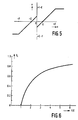
- Fig. 3 shows the output signal y on the output 17 as a function of the input signal x.
- the signal x is applied to the input 24 of a limiter circuit 23 having an output 25.
- Fig. 4 shows the output signal L as a function of the input signal x.
- the limiter circuit has a transfer function equal to unity.
- the output signal y of the quantizer 14 is applied to a first input 20 and the output signal L of the limiter 23 is applied to a second input 19 of a substractor 18, which produces the difference v between these signals on its output 21 and applies this difference to the input 27 of an at least 3rd-order loop filter 28, whose output 29 supplies the feedback signal Hv to the second input 12 of the summing circuit 10.
- the input signal i is converted into a 1-bit encoded signal with the aid of the quantizer 14, the quantization errors which are caused by the quantizer 14 and which are equal to the differences between the input signal and the output signal of the quantizer 14 being fed back to the input 15 of the quantizer 14 via the loop filter 28.
- the quantization errors may be regarded as white noise which is added to the input signal.
- the loop filter 28 has such a transfer characteristic that this noise within the signal band is reduced at the expense of an increase in noise outside this signal band, which last-mentioned noise can be removed by filtering the output signal of the encoding device.
- the limiter circuit 23 in combination with the special transfer function of the loop filter 28 then ensures that the encoding device does not exhibit any instabilities.
- the loop filter 28 has a transfer function given by: where n ⁇ 3 and 0 ⁇ a ⁇ b ⁇ 1.
- the constant b is approximately equal to unity and is suitably selected to equal unity.
- the stability of the encoding device in accordance with the invention will be considered in more detail, which device comprises a loop filter 28 having a transfer function given by equation (7).
- the stability is examined by means of the root-locus method.
- the encoding device is divided into a linear section comprising the quantizer 14, the limiter 23 and the summing circuit 18 with a transfer function G (see Fig. 2).
- Fig. 5 illustrates the relationship between the output signal v and the input signal x of the non-linear section, which can be derived simply from Figures 3 and 4. From these Figures it is evident that the transfer function G of the non-linear section depends on the magnitude of the input signal x and that the transfer function G ⁇ 1.
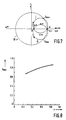
- the maximum value G L of the transfer function depends on the ratio between the value F to which the input signal x is limited by the limiter 23 and the quantization value E of the quantizer 14 and on the waveform of the signal x .
- Fig. 6 illustrates this dependence for a squarewave input signal.
- the arrows near the circles indicate the direction in which G increases from 0 to 1 along the circle.
- the value of the factor a also follows from the requirement that the quantization noise within the signal band should be small.
- the overall noise power added to the output signal of the encoding device by the quantizer is, as is known, equal to E2/3 for a quantization step 2E.
- Equation (11) For a given order n of the loop filter and a given sampling frequency fs i.e. a given ⁇ b, the noise power N i within the signal band is minimal if the factor C2(1-a)2 n is maximal.
- Fig. 13 illustrates the dependence of G max on the value of a .
- the value of a is again dictated by the requirement that the noise power within the signal band must be substantially minimal.
- the factor C2(1-a)8 must be substantially maximal.
- Fig. 14 illustrates the relationship between this factor and the value of the factor a . From this Figure a suitable value for a may be selected. The value of F to which the limiter 23 should limit the input signal of the loop filter 28 for this value of a can then be derived by means of Fig. 13 and Fig. 6.
- Fig. 14 also gives the relevant data for a 5th-order loop filter.
- Fig. 15 shows two modifications of the circuit shown in Fig. 2, in which identical parts bear the same reference numerals.
- the limiter 23 is arranged between the input 15 of the quantizer 14 and the input 27 of the loop filter 28.
- the limiter 23 limits the maximum value of the input signal v of the loop filter 8.
- Fig. 16 shows a modification of the diagram of Fig. 15a, the limiter 23 not being shown for a reason to be explained hereinafter.
- both the signal y applied to the input 19 of the subtractor 18 and the signal x applied to the input 19 of this subtractor are delayed by a factor Z ⁇ 1 by the delay means 30 and 31, respectively.
- the transfer function H of the loop filter 28 is multiplied by a factor Z.
- the signal x delayed by the delay means 31 is added directly to the input signal by applying this signal to an input 32 of the summing circuit 10 and the signal delayed by the delay means 30 is substracted directly from the input signal by applying this signal to an input 33 of the summing circuit.
- This modification has the advantage that the loop comprising the summing circuit 10 and the delay means 31 constitutes an integrator which is simple to realise in switched-capacitor technology. This integrator then also enables the limiting function of the limiter 23 (see Fig. 12a) to be realised simply.
- Fig. 17 the diagram of Fig. 16 has been converted into a diagram which is suitable for the use of switched capacitors.
- the delay means 30 and 31 with a delay Z ⁇ 1 are each split into two delay means 34, 36 and 35, 36 respectively each having a delay Z ⁇ 1/2, the delay means 36 being common to the delay means for the X signal and for the Y signal.
- the X signal delayed by Z ⁇ 1/2 by the delay means 36 is fed back to the input 32 of the summing circuit 10 via a delay means 37 with a delay Z ⁇ 1/2 in order to obtain an overall delay Z ⁇ 1 for this signal.
- Fig. 18 shows a switched-capacitor version of the encoding device which comprises a 3rd-order loop filter and is based on the diagram shown in Fig. 17.
- the section bearing the reference numeral 40 in Fig. 17 constitutes a switched-capacitor integrator.
- This integrator 40 comprises a capacitor C2 having one terminal which can be connected to earth or to the input for the input signal I via a switch S2, a capacitor C3 having one terminal which can be connected to earth or to the output 17 of the quantizer 14 via a switch S3, and a capacitor C4 having one terminal which can be connected to earth or to the output of the filter 28 via a switch S4.
- the other terminals of the capacitors C2, C3 and C4 can be connected to earth or to the inverting input of an amplifier 41 via a switch S1, the non-inverting input of this amplifier being connected to earth and the output of this amplifier being connected to its inverting input via a capacitor C1.
- the filter 28 comprises an amplifier 51 having a non-inverting input which is connected to earth and an inverting input which is connected to one terminal of a capacitor C5 whose other terminals can be connected to the output of the integrator 40 via a switch S5, the inverting input being also connected to one terminal of a capacitor C6 whose other terminal can be connected to the output of the quantizer 14 via a switch S6.
- By controlling the switches S5 and S6 in a specific manner in the present circuit these switches constitute the delay means 35 and 34 of Fig. 17.
- the output of the amplifier 51 is connected to the inverting input via a capacitor C7.
- the filter further comprises a capacitor C8 of which one terminal can be connected to earth or to the output of the amplifier 51 via a switch S7 and of which the other terminal can be connected to earth or to the inverting input of an amplifier 52 via a switch S8, the non-inverting input of said amplifier 52 being connected to earth and the output being connected to the inverting input via a capacitor C10.Further, said one terminal of the capacitor C8 is connected to one terminal of a capacitor C9 whose other terminal can be connected to earth or to the inverting input of the amplifier 51 via a switched S9.
- the other terminal of the capacitor C8 is further connected to one terminal of a capacitor C11 whose other terminal can be connected to earth or to the output of the amplifier 51 via a switch S11.
- the filter further comprises a capacitor C12 having one terminal which can be connected to earth or to the output of the amplifier 52 via a switch S10 and having another terminal which is connected to one terminal of the capacitor C15 whose other terminal is connected to one terminal of the capacitor C8, said other terminal of the capacitor C12 being also connected to one terminal of a capacitor C16 whose other terminal is connected to the other terminal of the capacitor C11.
- the other terminal of the capacitor C12 can be connected to earth or to the inverting input of an amplifier 53 via a switch S12, the non-inverting input of said amplifier 53 being connected to earth and the output being connected to the inverting input of the amplifier 53 via a capacitor C17 and to the inverting input of the amplifier 52 via a capacitor C18.
- the other terminal of the capacitor C8 and the capacitor C12 is connected to one terminal of a capacitor C14 and a capacitor C13 respectively, whose common other terminal can be connected to earth or to the input of the amplifier 53 via a switch S13.
- the switches S1-S14 are shown in the positions which they occupy during the clock phase ⁇ 1 of the clock signal by means of which the circuit is operated. During the clock phase ⁇ 2 of this clock signal the switches are in the other positions.
- the circuit operates as follows.
- the capacitors C2, C3 and C4 are charged to the input voltage i , the inverted output voltage y of the quantizer 14, and the output voltage of the filter 28 respectively.
- these capacitors C2, C3 and C4 are discharged via the capacitor C1, the voltage appearing on the output of the amplifier 41 being determined by said voltages and by the capacitance ratios between the capacitor C1 and the capacitors C2, C3 and C4.
- the voltage x on the output of the integrator is then delayed by half a clock period relative to the input voltage, which corresponds to a delay of Z ⁇ 1/2.
- the quantizer 14 is clocked out, so that the output signal -y is also delayed by half a clock period relative to the input voltage. It is to be noted that the voltage on the output 17 has already been inverted relative to that on the output 16, so that the voltage -y appears on the output 17.
- the switches S5 and S6 are closed, so that the voltages x and -y are delayed by a full clock period relative to the input signal, corresponding to a delay Z ⁇ 1, and applied to the filter 28.
- the capacitors C6 and C5 are both connected to the inverting input of amplifier 51, the sum of the voltage x and -y is then formed.
- the transfer function of the 3rd-order loop filter 28 is given by:
- the transfer function T(Z) is written as a product of a first-order transfer function and a second-order transfer function.
- the first-order transfer function is realized by the section 60 of the filter 28, which section basically comprises the combination of a differentiator and an integrator.
- the second-order transfer function is realized by the section 70 of the filter 28, which section basically comprises two integrators arranged in series.
- the coefficients in the transfer function are determined by the capacitance ratios of the capacitors. In integrated-circuit technology capacitance ratios can be realized with a high accuracy despite comparatively large tolerances in the capacitances of the individual capacitors.
- the output voltage of the integrator 40 also depends on the capacitance ratio between the capacitor C1 and the capacitors C2, C3 and C4. This capacitance ratio may now be selected in such a way that for a specific input voltage the output voltage of the amplifier 41 is limited by the power-supply voltage, so that the integrator itself acts as a limiter for the input signal.
- a further advantage of an at least third-order loop filter in a 1-bit encoding device for analog-to-digital conversion is that the annoying effects occurring in the first-order loop filter as a result of the d.c. offset on the input of the encoding device do not occur.
- Fig. 19 shows the basic diagram of a digital-to-analog converter in which an encoding device in accordance with the invention may be used.
- a 16-bit pulse-code-modulated signal with a sampling frequency F s is applied to the input 80 and is converted into, for example, a 24-bit signal with a sampling frequency 128.
- F s by means of an interpolating filter 81 comprising a up-sampler 82 and a low-pass filter 83.
- this signal is converted into, for example, a 1-bit encoded signal having a sampling frequency of 128.F s by means of an encoding device 84.
- this signal is converted into an analog signal, which appears on the output 86.
- the basic diagram of an encoding device in accordance with the invention for use in the device shown in Fig. 19 is identical to that shown in Fig. 2.
- the encoding device does not convert a discrete-time analog signal into a 1-bit signal but it converts a multi-bit digital-signal into an 1-bit signal.
- the quantizer 14, the loop filter 28, the limiter 23 and the summing circuits 10 and 8 are now of the digital type. However, for the operation of the encoding device it is irrelevant whether an analog or a digital signal is converted, so that the stability requirements for the encoding device remain the same.
- Fig. 20 shows a practical embodiment of such a device.
- the n-bit, for example 24-bit, input signal is applied to the digital summing circuit 10, in which it is added to the m-bit, for example 25-bit, output signal of the loop filter 28.
- the most significant bit of the k +1-bit, for example 25-bit, output signal of the summing circuit 10, i.e. the 25th or sign bit is applied to the quantizer 14 which comprises a digital comparator. For a positive value of this sign bit the output signal of the quantizer 14 is +E and for a negative value it is -E, corresponding to for example a logic "1" and a logic "0" respectively.
- the signal level +E expressed in the number of bits of the 25-bit input signal corresponds to the binary number 000100....0, of which only the most significant bit but 4 is 1. Expressed as this number of bits the signal level -E corresponds to the binary number 1110000....0. Therefore, for calculating the quantization error caused by the quantizer 14, only the four most significant bits 22 to 25 are required. These bits are applied to a device 90 which supplies the signal representing the difference between these four bits and the output signal level ⁇ E of the quantizer 14 expressed in the 4 most significant bits to the inputs 22-25 of the loop filter 28.
- the 21 least significant bits of the quantization error signal are applied directly from the output of the summing circuit 10 to the relevant inputs 1-21 of the loop filter 28.
- the total input signal of the loop filter 28 then represents the quantization error, i.e. the difference between the input signal and the output signal of the quantizer 14 expressed in the number of bits of the input signal.
- the device 90 also limits the maximum value of the input signal of the loop filter in order to maintain the encoding device stable.
- the signals a o , b o , c o and d o appearing on the outputs 22-25 of the device 90 then comply with, for example, the following relationships: where a, b, c and d are the output signals on the outputs 22-25 of the summing circuit 24.
- the device 90 produces a reset signal R on an output 91 for resetting the least significant bits 1-21 on the input of the loop filter 28 if the device 90 limits the output signal d o c o b o a o .
- This reset signal R complies with the following relationship: (17)
- R b.c.d. + b ⁇ . c ⁇ . d ⁇ + a ⁇ . c ⁇ . d ⁇
- the above logic expressions can be realised simply by means of standard logic elements.
- the input signal of the loop filter 28 is limited to a value 00100....0 for positive input signals and to a value 11100....0 for negative input signals.
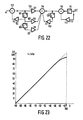
- Fig. 22 shows the circuit diagram of an example of a 3rd-order filter 28 whose transfer function is given by which may be written as:
- the filter comprises summing circuits, multipliers and delay means Z ⁇ 1.
- the input signal V is applied to a first input of a first summing circuit 100, a loop comprising a delay means 101 and a multiplier 102 with a coefficient 1/2 being arranged between the output and the second input, to form the first factor (1-1/2Z ⁇ 1) in the denominator of the transfer function.
- the output signal of the summing circuit 100 is further applied to a first input of a second summing circuit 104 via a multiplier 103 with a coefficient 3/2, to a second input via a delay means 101 followed by a multiplier 105 with a coefficient -9/4, and to a third input of the summing circuit 104 via delay means 101 and 106 followed by a multiplier 107 with a coefficient 7/8.
- the elements 101, 103-107 produce the factor 7/8Z ⁇ 2-9/4Z ⁇ 1+3/2.
- a second feedback loop comprising a delay means 108 and multiplier 109 with a coefficient 1/2 is arranged between the output and a fourth input of this summing circuit 104 to generate the second factor 1-1/2Z ⁇ 1.
- the output signal of the summing circuit 104 is applied to a first input of a third summing circuit 110, a third feedback loop comprising a delay means 111 followed by a multiplier 112 with a coefficient 1/2 being arranged between the output and a second input to generate the third factor 1-1/2Z ⁇ 1.
- the output signal of the summing circuit 110 is applied to the output of the filter via a delay means 111, which adds a factor Z ⁇ 1 to the transfer function, on which output the output signal H(Z)V appears, H(Z) being given by equation (19).
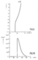
- the measured signal-to-noise ratio of the encoding device of Fig. 20 comprising a third-order loop filter 28 is plotted as a function of the power of a digitally generated sinewave input signal having a normalized frequency of 5.315.10 ⁇ 4.
- the 0-dB level corresponds to the maximum attainable output power E2/2 of the encoding device.
- Sm -7 dB.
- the invention is not limited to the embodiments shown. Within the scope of the invention as defined by the claims many modifications are conveivable to those skilled in the art.
- the input signal may also be added to the input signal of the filter instead of to the output signal of the filter.
Claims (14)
- Coder mit einem Quantisierer zum Umsetzen eines Eingangssignals in ein codiertes Einbitsignal, wobei der Quantisierer einen Eingang zum Empfangen des Eingangssignais und einen Ausgang zum Ausgeben des codierten Einbitsignals, und weiter einen Fehlerrückkoppler zum Rückkoppeln eines im Quantisierer verursachten Quantisierfehlersignals zum Quantisierereingang enthält, und der Fehlerrückkoppler ein Filter wenigstens dritter Ordnung mit einem Eingang und einem Ausgang besitzt, dadurch gekennzeichnet, daß die Übertragungsfunktion des Filters durch folgende Gleichung gegeben ist:

worin n ≧ 3 die Ordnung des Filters darstellt,
b eine Konstante im wesentlichen gleich eins is, und a eine Konstante ist, wobei 0 < a < b ist,
und daß der Coder einen Begrenzer zum Begrenzen des dem Filtereingang zugeführten Quantisierfehlersignals enthält. - Coder nach Anspruch 1,
dadurch gekennzeichnet, daß für ein Filter dritter Ordnung (n=3) die Konstante a einen Wert innerhalb des Intervalls 0,35 < a < b besitzt. - Coder nach Anspruch 2,
dadurch gekennzeichnet, daß der Wert der Konstante a im wesentlichen gleich a = 0,5 ist. - Coder nach Anspruch 1,
dadurch gekennzeichnet, daß für ein Filter vierter Ordnung (n=4) die Konstante a einen Wert innerhalb des Intervalls 0,6 < a < b besitzt. - Coder nach Anspruch 4,
dadurch gekennzeichnet, daß der Wert der Konstante a im wesentlichen gleich a = 0,66 ist. - Coder nach einem oder mehreren der vorangehenden Ansprüche, dadurch gekennzeichnet, daß das Eingangssignal ein Diskretzeit-Daueramplitudensignal ist.
- Coder nach einem oder mehreren der vorangehenden Ansprüche 1 bis 5, dadurch gekennzeichnet, daß das Eingangssignal ein Mehrbit-Digitalsignal ist.
- Coder nach Anspruch 6 oder 7,
dadurch gekennzeichnet, daß er noch folgende Elemente enthält:- einen ersten Summierer mit einem ersten Eingang zum Empfangen des Eingangssignals, mit einem zweiten Eingang zum Empfangen des Filterausgangssignals, und mit einem Ausgang zum Ausgeben des Summensignals der beiden Signale zum Eingang des Quantisierers,- eine zweiten Summierer mit einem ersten Eingang zum Empfangen des Ausgangssignals des Quantisierers, einem zweiten Eingang zum Empfangen des Ausgangs signals des ersten Summierers, und einem Ausgang zum Ausgeben des Unterschieds zwischen diesen beiden Signalen zum Filtereingang, und- daß der Begrenzer zwischen dem Ausgang des ersten Summierers und dem Filtereingang in einer ersten Schleife mit dem ersten Summierer, dem zweiten Summierer und dem Filter angeordnet ist. - Coder nach Anspruch 8, wenn abhängig vom Anspruch 6,
dadurch gekennzeichnet, daß- in der ersten Schleife mit dem ersten Summierer, dem zweiten Summierer und dem Filter ein erster Verzögerer zwischen dem Ausgang des ersten Summierers und dem ersten Eingang des zweiten Summierers zum Verzögern des Ausgangssignals des ersten Summierers um eine Taktperiode des Quantisierers angeordnet ist,- in der zweiten Schleife mit dem ersten Summierer, dem Quantisierer und dem Filter ein zweiter Verzögerer zwischen dem Ausgang des ersten Summierers und dem zweiten Eingang des zweiten Summierers angeordnet ist, und der zweite Summierer und der erste Summierer die gleiche Verzögerung besitzen,- der erste Summierer einen dritten Eingang zum Empfangen des um eine Taktperiode verzögerten Ausgangssignals des ersten Summierers besitzt,- der erste Summierer einen vierten Eingang zum Empfangen des um eine Taktperiode verzögerten Ausgangssignals des Quantisierers besitzt, und- die Übertragungsfunktion des Filters durch ZH(Z)⁻¹ gegeben ist. - Coder nach Anspruch 9,
dadurch gekennzeichnet, daß- in der ersten Schleife der erste Verzögerer einen dritten Verzögerer zum Verzögeren des Ausgangssignals des ersten Summierers um eine halbe Taktperiode zwischen dem Ausgang des ersten Summierers und dem Eingang des Quantisierers sowie einen vierten Verzögerer zum Verzögern des Ausgangssignals des Summierers um eine halbe Taktperiode zwischen dem Eingang des Quantisierers und dem ersten Eingang des zweiten Summierers enthält,- in der zweiten Schleife der zweite Verzögerer den ersten Verzögerer und einen fünften Verzögerer zum Verzögeren des Ausgangssignals des Quantisierers um eine halbe Taktperiode zwischen dem Ausgang des Quantisierers und dem zweiten Eingang des zweiten Summierers enthält, und- zwischen dem Ausgang des dritten Verzögerers und dem dritten Eingang des ersten Summierers ein sechster Verzögerer zum Verzögeren des Ausgangssignals des dritten Verzögerers um eine halbe Taktperiode angeordnet ist. - Coder nach Anspruch 10,
dadurch gekennzeichnet, daß die Anordnung mittels geschalteter Kondensatoren aufgebaut ist und in dieser Anordnung- die Schleife den ersten Summierer enthält, der dritte Verzögerer und der sechste Verzögerer einen Schaltkondensatorintegrator bilden, wobei die Signale am ersten Eingang, am zweiten Eingang und am vierten Eingang des ersten Summierers in der ersten Hälfte einer Taktperiode abgetastet werden und das Ausgangssignal des Integrators in der zweiten Hälfte einer Taktperiode an einen Ausgang des Integrators angelegt wird,- das Ausgangssignal des Quantisierers an den Ausgang des Quantisierers in der zweiten Hälfte einer Taktperiode gelangt,- der vierte Verzögerer einen ersten Schalter zum Anschließen des Integratorausgangs an einen ersten Eingang einer ersten in einer ersten Taktperiode enthält,- der fünfte Verzögerer einen zweiten Schalter zum Anschließen des Ausgangs des Quantisierers an einen zweiten Eingang des Filters in einer ersten Taktperiode enthält, und- das Filter ein Schaltkondensatorfilter mit einer Eingangsstufe ist, die die Summe der Signale am ersten Eingang und am zweiten Eingang des Filters bearbeitet. - Coder nach Anspruch 7,
dadurch gekennzeichnet, daß die Anordnung folgende Elemente enthält:- einen ersten Summierer mit einem ersten n-Bit-Eingang zum Empfangen eines n-Bit-Eingangssignals, einem zweiten m-Bit-Eingang zum Empfangen de m-Bit-Ausgangssignals des Filters und einem k+1-Bit-Ausgang zum Ausgeben des k+1-Bit-Summensignals dieser Signale,- ein Mittel zum Ausgeben des Bits des Summensignals mit höchster Wertigkeit zum Eingang des Quantisierers,- ein Mittel zum Ausgeben der k Bits mit niedrigster Wertigkeit zum k+1-Bit-Eingang des Filters, und- ein Mittel zum Ausgeben der 1 Bits des Summensignals mit höchster Wertigkeit an einen 1-Bit-Eingang einer logischen Schaltungsanordnung mit einem 1-Bit-Ausgang zum Ausgeben des 1-Bit-Unterschiedssignals des 1-Bit-Eingangssignals und des in 1 Bits des k+1-Eingangs des Filters ausgedrückten Quantisiererausgangssignals. - Analog/Digital-Wandler,
dadurch gekennzeichnet, daß er einen Coder nach einem oder mehreren der Ansprüche 1 bis 8 und 8 bis 11 enthält. - Digital/Analog-Wandler,
dadurch gekennzeichnet, daß er einen Coder nach einem der Ansprüche 1 bis 5, 7 und 12 enthält.
Applications Claiming Priority (2)
| Application Number | Priority Date | Filing Date | Title |
|---|---|---|---|
| NL8600862 | 1986-04-04 | ||
| NL8600862A NL8600862A (nl) | 1986-04-04 | 1986-04-04 | Kodeerinrichting. |
Publications (2)
| Publication Number | Publication Date |
|---|---|
| EP0241077A1 EP0241077A1 (de) | 1987-10-14 |
| EP0241077B1 true EP0241077B1 (de) | 1991-09-18 |
Family
ID=19847830
Family Applications (1)
| Application Number | Title | Priority Date | Filing Date |
|---|---|---|---|
| EP87200562A Expired - Lifetime EP0241077B1 (de) | 1986-04-04 | 1987-03-24 | Kodierungsvorrichtung |
Country Status (7)
| Country | Link |
|---|---|
| US (1) | US4692737A (de) |
| EP (1) | EP0241077B1 (de) |
| JP (1) | JPS62239618A (de) |
| KR (1) | KR950007465B1 (de) |
| CN (1) | CN1006672B (de) |
| DE (1) | DE3773033D1 (de) |
| NL (1) | NL8600862A (de) |
Families Citing this family (33)
| Publication number | Priority date | Publication date | Assignee | Title |
|---|---|---|---|---|
| DE3642168A1 (de) * | 1986-12-10 | 1988-06-16 | Philips Patentverwaltung | Digitale schaltungsanordnung zur verringerung des quantisierungsrauschens |
| JP2753126B2 (ja) * | 1990-09-20 | 1998-05-18 | 株式会社東芝 | ディジタル・シグマデルタ変調器 |
| NL9100379A (nl) * | 1991-03-01 | 1992-10-01 | Philips Nv | Sigma-deltamodulator. |
| US5140325A (en) * | 1991-05-14 | 1992-08-18 | Industrial Technology Research Institute | Sigma-delta analog-to-digital converters based on switched-capacitor differentiators and delays |
| US5345233A (en) * | 1992-03-30 | 1994-09-06 | Kabushiki Kaisha Toshiba | Digital Σ-Δ modulator |
| DE69431223T2 (de) * | 1993-06-29 | 2006-03-02 | Sony Corp. | Gerät und Verfahren zur Tonsignalübertragung |
| US5602874A (en) * | 1994-12-29 | 1997-02-11 | Motorola, Inc. | Method and apparatus for reducing quantization noise |
| US6993314B2 (en) | 1998-05-29 | 2006-01-31 | Silicon Laboratories Inc. | Apparatus for generating multiple radio frequencies in communication circuitry and associated methods |
| US6804497B2 (en) * | 2001-01-12 | 2004-10-12 | Silicon Laboratories, Inc. | Partitioned radio-frequency apparatus and associated methods |
| US7092675B2 (en) * | 1998-05-29 | 2006-08-15 | Silicon Laboratories | Apparatus and methods for generating radio frequencies in communication circuitry using multiple control signals |
| US7221921B2 (en) | 1998-05-29 | 2007-05-22 | Silicon Laboratories | Partitioning of radio-frequency apparatus |
| US7228109B2 (en) * | 2001-01-12 | 2007-06-05 | Silicon Laboratories Inc. | DC offset reduction in radio-frequency apparatus and associated methods |
| US7035607B2 (en) * | 1998-05-29 | 2006-04-25 | Silicon Laboratories Inc. | Systems and methods for providing an adjustable reference signal to RF circuitry |
| US6970717B2 (en) | 2001-01-12 | 2005-11-29 | Silicon Laboratories Inc. | Digital architecture for radio-frequency apparatus and associated methods |
| US7024221B2 (en) * | 2001-01-12 | 2006-04-04 | Silicon Laboratories Inc. | Notch filter for DC offset reduction in radio-frequency apparatus and associated methods |
| US7242912B2 (en) | 1998-05-29 | 2007-07-10 | Silicon Laboratories Inc. | Partitioning of radio-frequency apparatus |
| DE19854124C1 (de) * | 1998-11-24 | 2000-08-24 | Bosch Gmbh Robert | Sigma-Delta D/A-Wandler |
| US6903617B2 (en) | 2000-05-25 | 2005-06-07 | Silicon Laboratories Inc. | Method and apparatus for synthesizing high-frequency signals for wireless communications |
| US7138858B2 (en) | 2001-01-12 | 2006-11-21 | Silicon Laboratories, Inc. | Apparatus and methods for output buffer circuitry with constant output power in radio-frequency circuitry |
| US7031683B2 (en) * | 2001-01-12 | 2006-04-18 | Silicon Laboratories Inc. | Apparatus and methods for calibrating signal-processing circuitry |
| US7177610B2 (en) * | 2001-01-12 | 2007-02-13 | Silicon Laboratories Inc. | Calibrated low-noise current and voltage references and associated methods |
| US7158574B2 (en) * | 2001-01-12 | 2007-01-02 | Silicon Laboratories Inc. | Digital interface in radio-frequency apparatus and associated methods |
| US7035611B2 (en) * | 2001-01-12 | 2006-04-25 | Silicon Laboratories Inc. | Apparatus and method for front-end circuitry in radio-frequency apparatus |
| US20030232613A1 (en) * | 2001-01-12 | 2003-12-18 | Kerth Donald A. | Quadrature signal generation in radio-frequency apparatus and associated methods |
| AU2003220281A1 (en) * | 2002-03-15 | 2003-09-29 | Silicon Laboratories Inc. | Radio-frequency apparatus and associated methods |
| GB2408858B (en) * | 2003-12-05 | 2006-11-29 | Wolfson Ltd | Word length reduction circuit |
| US6956513B1 (en) * | 2004-10-22 | 2005-10-18 | Broadcom Corporation | Error feedback structure for delta-sigma modulators with improved stability |
| US7714675B2 (en) * | 2006-12-05 | 2010-05-11 | Broadcom Corporation | All digital Class-D modulator and its saturation protection techniques |
| US8816663B2 (en) * | 2010-02-26 | 2014-08-26 | Telefonaktiebolaget L M Ericsson (Publ) | Feedforward digital control unit for switched mode power supply and method thereof |
| WO2013120534A1 (en) | 2012-02-17 | 2013-08-22 | Telefonaktiebolaget L M Ericsson (Publ) | Voltage feed-forward compensation and voltage feedback compensation for switched mode power supplies |
| US9419562B1 (en) * | 2013-04-09 | 2016-08-16 | Cirrus Logic, Inc. | Systems and methods for minimizing noise in an amplifier |
| CN104601142A (zh) * | 2013-10-31 | 2015-05-06 | 横河电机株式会社 | 滤波方法、滤波器和闪变测试系统 |
| US10116323B2 (en) * | 2016-12-16 | 2018-10-30 | Mediatek Inc. | Analog-to-digital converter |
Family Cites Families (4)
| Publication number | Priority date | Publication date | Assignee | Title |
|---|---|---|---|---|
| US3624558A (en) * | 1970-01-16 | 1971-11-30 | Bell Telephone Labor Inc | Delta modulation encoder having double integration |
| JPS5120148B1 (de) * | 1971-05-19 | 1976-06-23 | ||
| US4035724A (en) * | 1974-05-08 | 1977-07-12 | Universite De Sherbrooke | Digital converter from continuous variable slope delta modulation to pulse code modulation |
| US4017849A (en) * | 1975-08-28 | 1977-04-12 | Bell Telephone Laboratories, Incorporated | Apparatus for analog to digital conversion |
-
1986
- 1986-04-04 NL NL8600862A patent/NL8600862A/nl not_active Application Discontinuation
- 1986-10-17 US US06/920,490 patent/US4692737A/en not_active Expired - Fee Related
-
1987
- 1987-03-24 DE DE8787200562T patent/DE3773033D1/de not_active Expired - Lifetime
- 1987-03-24 EP EP87200562A patent/EP0241077B1/de not_active Expired - Lifetime
- 1987-04-01 KR KR1019870003092A patent/KR950007465B1/ko active IP Right Grant
- 1987-04-01 CN CN87102565A patent/CN1006672B/zh not_active Expired
- 1987-04-04 JP JP62082234A patent/JPS62239618A/ja active Pending
Also Published As
| Publication number | Publication date |
|---|---|
| CN87102565A (zh) | 1987-10-14 |
| NL8600862A (nl) | 1987-11-02 |
| KR950007465B1 (ko) | 1995-07-11 |
| EP0241077A1 (de) | 1987-10-14 |
| US4692737A (en) | 1987-09-08 |
| JPS62239618A (ja) | 1987-10-20 |
| DE3773033D1 (de) | 1991-10-24 |
| CN1006672B (zh) | 1990-01-31 |
| KR870010696A (ko) | 1987-11-30 |
Similar Documents
| Publication | Publication Date | Title |
|---|---|---|
| EP0241077B1 (de) | Kodierungsvorrichtung | |
| US5103229A (en) | Plural-order sigma-delta analog-to-digital converters using both single-bit and multiple-bit quantization | |
| EP0368610B1 (de) | Verfahren zur Kaskadierung von mehreren Sigma-Delta-Modulatoren und ein Sigma-Delta-Modulatorsystem | |
| US5148166A (en) | Third order sigma delta oversampled analog-to-digital converter network with low component sensitivity | |
| US5084702A (en) | Plural-order sigma-delta analog-to-digital converter using both single-bit and multiple-bit quantizers | |
| US6535153B1 (en) | Adaptive sigma-delta modulation with one-bit quantization | |
| US5416481A (en) | Analog-to-digital converter with multi-level dither current input | |
| US5870048A (en) | Oversampling sigma-delta modulator | |
| EP0450947A2 (de) | Analog/Digital-Wandler | |
| EP0381764B1 (de) | Schaltung für analog-betätigung | |
| US5896101A (en) | Wide dynamic range delta sigma A/D converter | |
| JPH01204528A (ja) | A/d変換器 | |
| US5162799A (en) | A/d (analog-to-digital) converter | |
| US7453382B2 (en) | Method and apparatus for A/D conversion | |
| JP3371681B2 (ja) | 信号処理装置 | |
| WO1998056115A1 (en) | Analogue-to-digital conversion using frequency-modulated input or intermediate values | |
| US4999625A (en) | Generation of a digital correction signal to compensate for gain mismatches in a sigma delta modulator | |
| US5028924A (en) | Digital correction of gain mismatch in a sigma delta modulator | |
| JP3362718B2 (ja) | マルチビット−デルタシグマad変換器 | |
| JP3040546B2 (ja) | ノイズシェーピングa−d変換器 | |
| KR100214272B1 (ko) | 16-비트 오디오 아날로그-디지탈 변환기용 4차 ∑△변조기 | |
| Adams et al. | A novel architecture for reducing the sensitivity of multibit sigma-delta ADCs to DAC nonlinearity |
Legal Events
| Date | Code | Title | Description |
|---|---|---|---|
| PUAI | Public reference made under article 153(3) epc to a published international application that has entered the european phase |
Free format text: ORIGINAL CODE: 0009012 |
|
| AK | Designated contracting states |
Kind code of ref document: A1 Designated state(s): BE DE FR GB IT NL |
|
| 17P | Request for examination filed |
Effective date: 19880402 |
|
| 17Q | First examination report despatched |
Effective date: 19901109 |
|
| GRAA | (expected) grant |
Free format text: ORIGINAL CODE: 0009210 |
|
| AK | Designated contracting states |
Kind code of ref document: B1 Designated state(s): BE DE FR GB IT NL |
|
| PG25 | Lapsed in a contracting state [announced via postgrant information from national office to epo] |
Ref country code: NL Effective date: 19910918 Ref country code: BE Effective date: 19910918 |
|
| REF | Corresponds to: |
Ref document number: 3773033 Country of ref document: DE Date of ref document: 19911024 |
|
| ITF | It: translation for a ep patent filed |
Owner name: ING. C. GREGORJ S.P.A. |
|
| ET | Fr: translation filed | ||
| NLV1 | Nl: lapsed or annulled due to failure to fulfill the requirements of art. 29p and 29m of the patents act | ||
| PLBE | No opposition filed within time limit |
Free format text: ORIGINAL CODE: 0009261 |
|
| STAA | Information on the status of an ep patent application or granted ep patent |
Free format text: STATUS: NO OPPOSITION FILED WITHIN TIME LIMIT |
|
| 26N | No opposition filed | ||
| PGFP | Annual fee paid to national office [announced via postgrant information from national office to epo] |
Ref country code: GB Payment date: 19950228 Year of fee payment: 9 |
|
| PGFP | Annual fee paid to national office [announced via postgrant information from national office to epo] |
Ref country code: FR Payment date: 19950329 Year of fee payment: 9 |
|
| ITPR | It: changes in ownership of a european patent |
Owner name: CAMBIO RAGIONE SOCIALE;PHILIPS ELECTRONICS N.V. |
|
| PGFP | Annual fee paid to national office [announced via postgrant information from national office to epo] |
Ref country code: DE Payment date: 19950529 Year of fee payment: 9 |
|
| REG | Reference to a national code |
Ref country code: FR Ref legal event code: CD |
|
| PG25 | Lapsed in a contracting state [announced via postgrant information from national office to epo] |
Ref country code: GB Effective date: 19960324 |
|
| GBPC | Gb: european patent ceased through non-payment of renewal fee |
Effective date: 19960324 |
|
| PG25 | Lapsed in a contracting state [announced via postgrant information from national office to epo] |
Ref country code: FR Effective date: 19961129 |
|
| PG25 | Lapsed in a contracting state [announced via postgrant information from national office to epo] |
Ref country code: DE Effective date: 19961203 |
|
| REG | Reference to a national code |
Ref country code: FR Ref legal event code: ST |
|
| PG25 | Lapsed in a contracting state [announced via postgrant information from national office to epo] |
Ref country code: IT Free format text: LAPSE BECAUSE OF NON-PAYMENT OF DUE FEES;WARNING: LAPSES OF ITALIAN PATENTS WITH EFFECTIVE DATE BEFORE 2007 MAY HAVE OCCURRED AT ANY TIME BEFORE 2007. THE CORRECT EFFECTIVE DATE MAY BE DIFFERENT FROM THE ONE RECORDED. Effective date: 20050324 |