EP0233138A1 - Verfahren zur Herstellung einer bespielten plattenförmigen Matrize - Google Patents
Verfahren zur Herstellung einer bespielten plattenförmigen Matrize Download PDFInfo
- Publication number
- EP0233138A1 EP0233138A1 EP87730010A EP87730010A EP0233138A1 EP 0233138 A1 EP0233138 A1 EP 0233138A1 EP 87730010 A EP87730010 A EP 87730010A EP 87730010 A EP87730010 A EP 87730010A EP 0233138 A1 EP0233138 A1 EP 0233138A1
- Authority
- EP
- European Patent Office
- Prior art keywords
- layer
- information
- carrier layer
- recorded
- information carrier
- Prior art date
- Legal status (The legal status is an assumption and is not a legal conclusion. Google has not performed a legal analysis and makes no representation as to the accuracy of the status listed.)
- Withdrawn
Links
- 238000004519 manufacturing process Methods 0.000 title claims abstract description 13
- 239000011159 matrix material Substances 0.000 title abstract description 7
- 239000011521 glass Substances 0.000 claims abstract description 28
- 238000000034 method Methods 0.000 claims abstract description 28
- PXHVJJICTQNCMI-UHFFFAOYSA-N Nickel Chemical compound [Ni] PXHVJJICTQNCMI-UHFFFAOYSA-N 0.000 claims abstract description 20
- 229910000510 noble metal Inorganic materials 0.000 claims abstract description 11
- 229910052759 nickel Inorganic materials 0.000 claims abstract description 10
- 238000005520 cutting process Methods 0.000 claims abstract description 8
- 238000004049 embossing Methods 0.000 claims abstract description 4
- 239000000126 substance Substances 0.000 claims abstract 5
- RYGMFSIKBFXOCR-UHFFFAOYSA-N Copper Chemical compound [Cu] RYGMFSIKBFXOCR-UHFFFAOYSA-N 0.000 claims description 13
- 229910052802 copper Inorganic materials 0.000 claims description 13
- 239000010949 copper Substances 0.000 claims description 13
- PCHJSUWPFVWCPO-UHFFFAOYSA-N gold Chemical compound [Au] PCHJSUWPFVWCPO-UHFFFAOYSA-N 0.000 claims description 10
- 229910052737 gold Inorganic materials 0.000 claims description 10
- 239000010931 gold Substances 0.000 claims description 10
- BASFCYQUMIYNBI-UHFFFAOYSA-N platinum Chemical compound [Pt] BASFCYQUMIYNBI-UHFFFAOYSA-N 0.000 claims description 8
- 229910000906 Bronze Inorganic materials 0.000 claims description 7
- ATJFFYVFTNAWJD-UHFFFAOYSA-N Tin Chemical compound [Sn] ATJFFYVFTNAWJD-UHFFFAOYSA-N 0.000 claims description 7
- 239000010974 bronze Substances 0.000 claims description 7
- KUNSUQLRTQLHQQ-UHFFFAOYSA-N copper tin Chemical compound [Cu].[Sn] KUNSUQLRTQLHQQ-UHFFFAOYSA-N 0.000 claims description 7
- 229910052751 metal Inorganic materials 0.000 claims description 7
- 239000002184 metal Substances 0.000 claims description 7
- RBTARNINKXHZNM-UHFFFAOYSA-K iron trichloride Chemical compound Cl[Fe](Cl)Cl RBTARNINKXHZNM-UHFFFAOYSA-K 0.000 claims description 6
- VEXZGXHMUGYJMC-UHFFFAOYSA-N Hydrochloric acid Chemical compound Cl VEXZGXHMUGYJMC-UHFFFAOYSA-N 0.000 claims description 4
- 229910052697 platinum Inorganic materials 0.000 claims description 4
- 229910021578 Iron(III) chloride Inorganic materials 0.000 claims description 3
- 238000000926 separation method Methods 0.000 claims description 3
- 239000000203 mixture Substances 0.000 claims 2
- 229910000881 Cu alloy Inorganic materials 0.000 claims 1
- 229910045601 alloy Inorganic materials 0.000 claims 1
- 239000000956 alloy Substances 0.000 claims 1
- 238000001704 evaporation Methods 0.000 claims 1
- 230000008020 evaporation Effects 0.000 claims 1
- 239000010953 base metal Substances 0.000 abstract description 3
- 239000010410 layer Substances 0.000 description 71
- 229920002120 photoresistant polymer Polymers 0.000 description 16
- BQCADISMDOOEFD-UHFFFAOYSA-N Silver Chemical compound [Ag] BQCADISMDOOEFD-UHFFFAOYSA-N 0.000 description 6
- 239000012790 adhesive layer Substances 0.000 description 6
- 229910052709 silver Inorganic materials 0.000 description 6
- 239000004332 silver Substances 0.000 description 6
- 238000005516 engineering process Methods 0.000 description 5
- 238000011161 development Methods 0.000 description 4
- 230000018109 developmental process Effects 0.000 description 4
- 238000009713 electroplating Methods 0.000 description 4
- 239000000969 carrier Substances 0.000 description 3
- 239000012876 carrier material Substances 0.000 description 3
- VEXZGXHMUGYJMC-UHFFFAOYSA-M Chloride anion Chemical compound [Cl-] VEXZGXHMUGYJMC-UHFFFAOYSA-M 0.000 description 2
- XEEYBQQBJWHFJM-UHFFFAOYSA-N Iron Chemical compound [Fe] XEEYBQQBJWHFJM-UHFFFAOYSA-N 0.000 description 2
- 239000000428 dust Substances 0.000 description 2
- 238000005530 etching Methods 0.000 description 2
- 230000003287 optical effect Effects 0.000 description 2
- 239000002245 particle Substances 0.000 description 2
- 238000003860 storage Methods 0.000 description 2
- 239000000853 adhesive Substances 0.000 description 1
- 230000001070 adhesive effect Effects 0.000 description 1
- 239000012298 atmosphere Substances 0.000 description 1
- 238000001311 chemical methods and process Methods 0.000 description 1
- 230000003749 cleanliness Effects 0.000 description 1
- 229910003460 diamond Inorganic materials 0.000 description 1
- 239000010432 diamond Substances 0.000 description 1
- 229910052742 iron Inorganic materials 0.000 description 1
- 239000004922 lacquer Substances 0.000 description 1
- 239000000463 material Substances 0.000 description 1
- 239000010970 precious metal Substances 0.000 description 1
- 238000003825 pressing Methods 0.000 description 1
- 239000002904 solvent Substances 0.000 description 1
- 239000000758 substrate Substances 0.000 description 1
- 238000011179 visual inspection Methods 0.000 description 1
- 238000005406 washing Methods 0.000 description 1
Images
Classifications
-
- G—PHYSICS
- G11—INFORMATION STORAGE
- G11B—INFORMATION STORAGE BASED ON RELATIVE MOVEMENT BETWEEN RECORD CARRIER AND TRANSDUCER
- G11B23/00—Record carriers not specific to the method of recording or reproducing; Accessories, e.g. containers, specially adapted for co-operation with the recording or reproducing apparatus ; Intermediate mediums; Apparatus or processes specially adapted for their manufacture
- G11B23/0057—Intermediate mediums, i.e. mediums provided with an information structure not specific to the method of reproducing or duplication such as matrixes for mechanical pressing of an information structure ; record carriers having a relief information structure provided with or included in layers not specific for a single reproducing method; apparatus or processes specially adapted for their manufacture
-
- G—PHYSICS
- G11—INFORMATION STORAGE
- G11B—INFORMATION STORAGE BASED ON RELATIVE MOVEMENT BETWEEN RECORD CARRIER AND TRANSDUCER
- G11B3/00—Recording by mechanical cutting, deforming or pressing, e.g. of grooves or pits; Reproducing by mechanical sensing; Record carriers therefor
- G11B3/68—Record carriers
- G11B3/685—Intermediate mediums
Definitions
- the invention relates to a method for producing a recorded plate-shaped die according to the preamble of claim 1.
- the invention further relates to a pre-recorded plate-shaped die and an unrecorded information carrier according to the preambles of claims 10 and 11.
- the detached sandwich cannot be used directly for duplication yet, but forms an intermediate stage.
- this intermediate stage is particularly suitable for storage and transport, since it offers no access to the information signal of the information carrier layer, since the area containing the information is embedded on both sides in metal layers.
- the glass carrier can then be detached from the photoresist layer, so that the residues of the photoresist layer can be removed from the glass carrier together with the adhesive layer or from the silver layer 4 by suitable solvents.
- the signal marking is now in a raised form as a negative and can be reproduced in subsequent electroplating stages.
- the task of the adhesive layer 2 is essentially to give the photoresist layer on the one hand a better adhesive base to the glass, so as not to apply one later Nickel layer and the stresses caused thereby to cause detachment of the photoresist layer, on the other hand to prevent striking on the glass surface when the silver layer 4 is applied, since otherwise the silver layer would adhere to the glass surface.
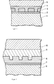
- FIG. 2 shows a cross section through a die according to the invention in a cross-sectional representation that is not to scale.
- a thin tin bronze layer with a thickness of approximately 20 nm is first evaporated on a glass support 6 with a thickness of 6-8 mm in a high vacuum.
- a pure copper layer is deposited thereon in a high vacuum with a thickness of approximately 100-300 nm. The copper applied in this way is sufficiently ductile to enable an information signal to be cut or impressed.
- the copper layer used to cut or stamp the information can be etched off in a simple iron (III) chloride bath.
- a little hydrochloric acid is preferably added to this bath.
- a suitable batch of such a bath contains 50 g FeCla x 6 H 2 0, 25 ml HC1 (25%), 1 1 H 2 0.
- the iron-III chloride bath cannot attack the intermediate layer 9 made of noble metal, namely gold or platinum or another noble metal, only the copper layer is etched away. The recorded information signal therefore emerges in the gold layer without any mechanical damage or shape change. The copper layer is completely removed by the iron III chloride bath.
Landscapes
- Manufacturing Optical Record Carriers (AREA)
Applications Claiming Priority (2)
| Application Number | Priority Date | Filing Date | Title |
|---|---|---|---|
| DE19863604237 DE3604237A1 (de) | 1986-02-11 | 1986-02-11 | Verfahren zur herstellung einer bespielten plattenfoermigen matrize, eine bespielte plattenfoermige matrize sowie deren unbespielte vorstufe |
| DE3604237 | 1986-02-11 |
Publications (1)
| Publication Number | Publication Date |
|---|---|
| EP0233138A1 true EP0233138A1 (de) | 1987-08-19 |
Family
ID=6293849
Family Applications (1)
| Application Number | Title | Priority Date | Filing Date |
|---|---|---|---|
| EP87730010A Withdrawn EP0233138A1 (de) | 1986-02-11 | 1987-01-31 | Verfahren zur Herstellung einer bespielten plattenförmigen Matrize |
Country Status (7)
| Country | Link |
|---|---|
| US (1) | US4814047A (show.php) |
| EP (1) | EP0233138A1 (show.php) |
| JP (1) | JPS63502703A (show.php) |
| AU (1) | AU6937487A (show.php) |
| DE (1) | DE3604237A1 (show.php) |
| DK (1) | DK522287A (show.php) |
| WO (1) | WO1987004837A1 (show.php) |
Families Citing this family (2)
| Publication number | Priority date | Publication date | Assignee | Title |
|---|---|---|---|---|
| DE3737483A1 (de) * | 1987-11-05 | 1989-05-18 | Philips & Du Pont Optical | Verfahren zur wiederverwendung von glas-substraten fuer optisch auslesbare dichtspeichermaster |
| US6007652A (en) * | 1990-11-05 | 1999-12-28 | Murata Manufacturing Co., Ltd. | Method of preparing metal thin film having excellent transferability |
Citations (2)
| Publication number | Priority date | Publication date | Assignee | Title |
|---|---|---|---|---|
| DE2137888A1 (de) * | 1970-08-13 | 1973-02-08 | Licentia Gmbh | Folie zur herstellung von plattenfoermigen informationstraegern, z.b. von schall- oder bildplatten |
| DE2721608A1 (de) * | 1977-05-13 | 1978-11-16 | Bosch Gmbh Robert | Verfahren zur herstellung einer nachbildungsmatrize |
Family Cites Families (3)
| Publication number | Priority date | Publication date | Assignee | Title |
|---|---|---|---|---|
| US4402798A (en) * | 1982-02-16 | 1983-09-06 | Rca Corporation | Method for the manufacture of a metallic recording substrate for a capacitance electronic disc and the recording substrate obtained thereby |
| NL8303315A (nl) * | 1982-10-14 | 1984-05-01 | Philips Nv | Methode voor de vervaardiging van een moedermatrijs. |
| US4469563A (en) * | 1983-08-22 | 1984-09-04 | Rca Corporation | Process for treating high-density information disc recording substrates |
-
1986
- 1986-02-11 DE DE19863604237 patent/DE3604237A1/de active Granted
-
1987
- 1987-01-31 WO PCT/DE1987/000038 patent/WO1987004837A1/de not_active Ceased
- 1987-01-31 EP EP87730010A patent/EP0233138A1/de not_active Withdrawn
- 1987-01-31 JP JP62500974A patent/JPS63502703A/ja active Pending
- 1987-01-31 AU AU69374/87A patent/AU6937487A/en not_active Abandoned
- 1987-02-10 US US07/012,899 patent/US4814047A/en not_active Expired - Fee Related
- 1987-10-06 DK DK522287A patent/DK522287A/da not_active Application Discontinuation
Patent Citations (2)
| Publication number | Priority date | Publication date | Assignee | Title |
|---|---|---|---|---|
| DE2137888A1 (de) * | 1970-08-13 | 1973-02-08 | Licentia Gmbh | Folie zur herstellung von plattenfoermigen informationstraegern, z.b. von schall- oder bildplatten |
| DE2721608A1 (de) * | 1977-05-13 | 1978-11-16 | Bosch Gmbh Robert | Verfahren zur herstellung einer nachbildungsmatrize |
Non-Patent Citations (6)
| Title |
|---|
| PATENT ABSTRACTS OF JAPAN, Band 2, Nr. 82, 30. Juni 1978, Seite 3413 (E-78); & JP-A-53 046 004 (FUJI SHASHIN FILM K.K.) 25-04-1978 * |
| PATENT ABSTRACTS OF JAPAN, Band 7, Nr. 270 (P-240)[1415], 2. Dezember 1983; & JP-A-58 150 148 (TOKYO SHIBAURA DENKI K.K.) 06-09-1983 * |
| PATENT ABSTRACTS OF JAPAN, Band 8, Nr. 165 (P-291)[1602], 31. Juli 1984; & JP-A-59 060 702 (TOSHIBA K.K.) 06-04-1984 * |
| PATENT ABSTRACTS OF JAPAN, Band 8, Nr. 97 (P-272)[1534], 8. Mai 1984; & JP-A-59 008 149 (MATSUSHITA DENKI SANGYO K.K.) 17-01-1984 * |
| PROCEEDINGS OF SPIE, Band 421, Arlington, Virginia, 8.-9. Juni 1983, Seiten 85-90, SPIE, US; R. IMANAKA et al.: "Optical disc memory system" * |
| WIRELESS WORLD, Band 89, Nr. 1566, März 1983, Seite 60, Olchester, GB; "Mastering metals for mothers" * |
Also Published As
| Publication number | Publication date |
|---|---|
| WO1987004837A1 (fr) | 1987-08-13 |
| DK522287D0 (da) | 1987-10-06 |
| AU6937487A (en) | 1987-08-25 |
| US4814047A (en) | 1989-03-21 |
| JPS63502703A (ja) | 1988-10-06 |
| DK522287A (da) | 1987-10-06 |
| DE3604237C2 (show.php) | 1988-01-14 |
| DE3604237A1 (de) | 1987-08-13 |
Similar Documents
| Publication | Publication Date | Title |
|---|---|---|
| DE3486405T2 (de) | Optisches Speicherelement. | |
| DE3511712C2 (de) | Plattenförmiger Informationsträger und Verfahren zu seiner Herstellung | |
| DE69215532T2 (de) | Optische datenaufzeichnungensscheibe | |
| DE69612929T2 (de) | Doppelseitige optisch lesbare Informationsaufzeichnungsplattenstapel und Verfahren zu deren Herstellung | |
| DE69127058T2 (de) | Herstellungsverfahren einer Matrize | |
| DE2642342C2 (de) | Verfahren zum Einschreiben von Informationen mittels eines Einschreibstrahlenbündels auf eine um eine Achse rotierende, optische Speicherplatte und optische Speicherplatte zur Durchführung dieses Verfahrens | |
| DE3125717C2 (de) | Reflektierendes Datenspeicher- und Aufzeichungsmedium | |
| DE3844011A1 (de) | Wiederaufbereitbares formwerkzeug und dieses verwendendes formverfahren | |
| DE19830293A1 (de) | Stempel für optische Disks und Verfahren/Systeme zur Herstellung der Stempel | |
| DE3882345T2 (de) | Verfahren und Photomaske zur Herstellung eines optischen Speicherelementes. | |
| DE69230595T2 (de) | Optische Platte mit metallischer Reflektionsschicht | |
| DE69124477T2 (de) | Prägemetallform und Verfahren zu ihrer Herstellung | |
| DE3306538A1 (de) | Platte zum aufzeichnen von optischen daten | |
| DE3604237C2 (show.php) | ||
| DE69016603T2 (de) | Verfahren zur Herstellung einer optischen Speicherplatte. | |
| DE69527221T2 (de) | Herstellung einer Originalplatte oder einer optischen Platte | |
| DE69418503T2 (de) | Urplatten zur Herstellung von Matrizen, insbesondere für optische Platten, und Verfahren zu deren Herstellung | |
| EP0738573A2 (de) | Matrize zum Abformen von Schallaufzeichnungen und Verfahren zu ihrer Herstellung | |
| EP0058894A1 (de) | Kratzfeste, antistatische Ton- und Bildträger und Verfahren zu ihrer Herstellung | |
| JP3105977B2 (ja) | 微細凹凸パターン成形用成形型 | |
| DE69315096T2 (de) | Verfahren zur Herstellung von Matrizen, insbesondere zur Herstellung von optichen Platten | |
| DE3842227C2 (de) | Verfahren zur Herstellung von Vervielfältigungsstücken einer mit digitalen Tonsignalen bespielten Masterplatte | |
| DE2342285C3 (de) | Verfahren zur Herstellung eines scheibenförmigen Datenträgers | |
| DE2342285B2 (de) | Verfahren zur herstellung eines scheibenfoermigen datentraegers | |
| DE3825590A1 (de) | Master fuer optische speichermedien |
Legal Events
| Date | Code | Title | Description |
|---|---|---|---|
| PUAI | Public reference made under article 153(3) epc to a published international application that has entered the european phase |
Free format text: ORIGINAL CODE: 0009012 |
|
| AK | Designated contracting states |
Kind code of ref document: A1 Designated state(s): AT BE CH DE ES FR GB GR IT LI NL SE |
|
| 17P | Request for examination filed |
Effective date: 19871014 |
|
| 17Q | First examination report despatched |
Effective date: 19890518 |
|
| STAA | Information on the status of an ep patent application or granted ep patent |
Free format text: STATUS: THE APPLICATION IS DEEMED TO BE WITHDRAWN |
|
| 18D | Application deemed to be withdrawn |
Effective date: 19890929 |
|
| RIN1 | Information on inventor provided before grant (corrected) |
Inventor name: JOSCHKO, GUENTER, DIPL.-PHYS. Inventor name: REDLICH, HORST, ING. |