EP0232702A2 - Einrichtung und Verfahren zum Steuern eines Leistungskonverters - Google Patents
Einrichtung und Verfahren zum Steuern eines Leistungskonverters Download PDFInfo
- Publication number
- EP0232702A2 EP0232702A2 EP87100048A EP87100048A EP0232702A2 EP 0232702 A2 EP0232702 A2 EP 0232702A2 EP 87100048 A EP87100048 A EP 87100048A EP 87100048 A EP87100048 A EP 87100048A EP 0232702 A2 EP0232702 A2 EP 0232702A2
- Authority
- EP
- European Patent Office
- Prior art keywords
- pulse patterns
- power converter
- control signals
- timings
- controlling
- Prior art date
- Legal status (The legal status is an assumption and is not a legal conclusion. Google has not performed a legal analysis and makes no representation as to the accuracy of the status listed.)
- Granted
Links
Images


Classifications
-
- H—ELECTRICITY
- H02—GENERATION; CONVERSION OR DISTRIBUTION OF ELECTRIC POWER
- H02M—APPARATUS FOR CONVERSION BETWEEN AC AND AC, BETWEEN AC AND DC, OR BETWEEN DC AND DC, AND FOR USE WITH MAINS OR SIMILAR POWER SUPPLY SYSTEMS; CONVERSION OF DC OR AC INPUT POWER INTO SURGE OUTPUT POWER; CONTROL OR REGULATION THEREOF
- H02M5/00—Conversion of AC power input into AC power output, e.g. for change of voltage, for change of frequency, for change of number of phases
- H02M5/40—Conversion of AC power input into AC power output, e.g. for change of voltage, for change of frequency, for change of number of phases with intermediate conversion into DC
- H02M5/42—Conversion of AC power input into AC power output, e.g. for change of voltage, for change of frequency, for change of number of phases with intermediate conversion into DC by static converters
- H02M5/44—Conversion of AC power input into AC power output, e.g. for change of voltage, for change of frequency, for change of number of phases with intermediate conversion into DC by static converters using discharge tubes or semiconductor devices to convert the intermediate DC into AC
- H02M5/443—Conversion of AC power input into AC power output, e.g. for change of voltage, for change of frequency, for change of number of phases with intermediate conversion into DC by static converters using discharge tubes or semiconductor devices to convert the intermediate DC into AC using devices of a thyratron or thyristor type requiring extinguishing means
- H02M5/45—Conversion of AC power input into AC power output, e.g. for change of voltage, for change of frequency, for change of number of phases with intermediate conversion into DC by static converters using discharge tubes or semiconductor devices to convert the intermediate DC into AC using devices of a thyratron or thyristor type requiring extinguishing means using semiconductor devices only
-
- H—ELECTRICITY
- H02—GENERATION; CONVERSION OR DISTRIBUTION OF ELECTRIC POWER
- H02M—APPARATUS FOR CONVERSION BETWEEN AC AND AC, BETWEEN AC AND DC, OR BETWEEN DC AND DC, AND FOR USE WITH MAINS OR SIMILAR POWER SUPPLY SYSTEMS; CONVERSION OF DC OR AC INPUT POWER INTO SURGE OUTPUT POWER; CONTROL OR REGULATION THEREOF
- H02M5/00—Conversion of AC power input into AC power output, e.g. for change of voltage, for change of frequency, for change of number of phases
- H02M5/40—Conversion of AC power input into AC power output, e.g. for change of voltage, for change of frequency, for change of number of phases with intermediate conversion into DC
- H02M5/42—Conversion of AC power input into AC power output, e.g. for change of voltage, for change of frequency, for change of number of phases with intermediate conversion into DC by static converters
- H02M5/44—Conversion of AC power input into AC power output, e.g. for change of voltage, for change of frequency, for change of number of phases with intermediate conversion into DC by static converters using discharge tubes or semiconductor devices to convert the intermediate DC into AC
- H02M5/453—Conversion of AC power input into AC power output, e.g. for change of voltage, for change of frequency, for change of number of phases with intermediate conversion into DC by static converters using discharge tubes or semiconductor devices to convert the intermediate DC into AC using devices of a triode or transistor type requiring continuous application of a control signal
- H02M5/458—Conversion of AC power input into AC power output, e.g. for change of voltage, for change of frequency, for change of number of phases with intermediate conversion into DC by static converters using discharge tubes or semiconductor devices to convert the intermediate DC into AC using devices of a triode or transistor type requiring continuous application of a control signal using semiconductor devices only
- H02M5/4585—Conversion of AC power input into AC power output, e.g. for change of voltage, for change of frequency, for change of number of phases with intermediate conversion into DC by static converters using discharge tubes or semiconductor devices to convert the intermediate DC into AC using devices of a triode or transistor type requiring continuous application of a control signal using semiconductor devices only having a rectifier with controlled elements
-
- H—ELECTRICITY
- H02—GENERATION; CONVERSION OR DISTRIBUTION OF ELECTRIC POWER
- H02M—APPARATUS FOR CONVERSION BETWEEN AC AND AC, BETWEEN AC AND DC, OR BETWEEN DC AND DC, AND FOR USE WITH MAINS OR SIMILAR POWER SUPPLY SYSTEMS; CONVERSION OF DC OR AC INPUT POWER INTO SURGE OUTPUT POWER; CONTROL OR REGULATION THEREOF
- H02M7/00—Conversion of AC power input into DC power output; Conversion of DC power input into AC power output
- H02M7/02—Conversion of AC power input into DC power output without possibility of reversal
- H02M7/04—Conversion of AC power input into DC power output without possibility of reversal by static converters
- H02M7/12—Conversion of AC power input into DC power output without possibility of reversal by static converters using discharge tubes with control electrode or semiconductor devices with control electrode
- H02M7/21—Conversion of AC power input into DC power output without possibility of reversal by static converters using discharge tubes with control electrode or semiconductor devices with control electrode using devices of a triode or transistor type requiring continuous application of a control signal
-
- H—ELECTRICITY
- H02—GENERATION; CONVERSION OR DISTRIBUTION OF ELECTRIC POWER
- H02M—APPARATUS FOR CONVERSION BETWEEN AC AND AC, BETWEEN AC AND DC, OR BETWEEN DC AND DC, AND FOR USE WITH MAINS OR SIMILAR POWER SUPPLY SYSTEMS; CONVERSION OF DC OR AC INPUT POWER INTO SURGE OUTPUT POWER; CONTROL OR REGULATION THEREOF
- H02M7/00—Conversion of AC power input into DC power output; Conversion of DC power input into AC power output
- H02M7/42—Conversion of DC power input into AC power output without possibility of reversal
- H02M7/44—Conversion of DC power input into AC power output without possibility of reversal by static converters
- H02M7/48—Conversion of DC power input into AC power output without possibility of reversal by static converters using discharge tubes with control electrode or semiconductor devices with control electrode
- H02M7/53—Conversion of DC power input into AC power output without possibility of reversal by static converters using discharge tubes with control electrode or semiconductor devices with control electrode using devices of a triode or transistor type requiring continuous application of a control signal
- H02M7/537—Conversion of DC power input into AC power output without possibility of reversal by static converters using discharge tubes with control electrode or semiconductor devices with control electrode using devices of a triode or transistor type requiring continuous application of a control signal using semiconductor devices only, e.g. single switched pulse inverters
- H02M7/5387—Conversion of DC power input into AC power output without possibility of reversal by static converters using discharge tubes with control electrode or semiconductor devices with control electrode using devices of a triode or transistor type requiring continuous application of a control signal using semiconductor devices only, e.g. single switched pulse inverters in a bridge configuration
- H02M7/53871—Conversion of DC power input into AC power output without possibility of reversal by static converters using discharge tubes with control electrode or semiconductor devices with control electrode using devices of a triode or transistor type requiring continuous application of a control signal using semiconductor devices only, e.g. single switched pulse inverters in a bridge configuration with automatic control of output voltage or current
- H02M7/53873—Conversion of DC power input into AC power output without possibility of reversal by static converters using discharge tubes with control electrode or semiconductor devices with control electrode using devices of a triode or transistor type requiring continuous application of a control signal using semiconductor devices only, e.g. single switched pulse inverters in a bridge configuration with automatic control of output voltage or current with digital control
Definitions
- This invention relates to a power converter such as an inverter and more particularly to a method and apparatus for controlling a power converter which is preferably used for a winding machine for an elevator.
- Inverters have been widely used for controlling elevators using induction motors for driving winding machines. Power converters including such inverters have been mainly controlled by analog control systems. Such analog control systems, however, provide several problems including their output fluctuation and limited setting accuracy; the output fluctuation will be caused by the secular changes of several components used in the systems.
- pulse width data are previously stored, during the absence of the processing by a microcomputer, in a timer externally attatched in the bus of the microcomputer, and the microcomputer, when interrupted by the timer, only supplies an actuation instruction to the timer, thereafter performing a scheduled processing, so that the microcomputer doesn't need to perform the output processing.
- This system permits the microcomputer to concentrate on the processings of the reference to a data table for acquisition of the pulse width data and the data working so that the performance thereof may be improved.
- the former system involves the following problems since a timer, distribution circuit, etc. must be externally provided.
- the latter system involves the problem that because of the increased amount of processing in the microcomputer, the minimum pulse width of the control signals to be supplied to the switching elements of the power converter cannot be reduced less than the interruption processing time in the microcomputer.
- An object of this invention is to provide a method and apparatus for controlling a power converter which is capable of solving the aforesaid problems of the prior art and generating pulse outputs with their pulse width being sufficiently narrow, in a simplified circuit construction using a microcomputer.
- pulse patterns for creating control signals to be supplied to the switching elements of a power converter are previously and successively created, a schedule processing of successively setting, as pairs, the pulse patterns and times when they are to be supplied is executed and the control signals are successively output at the times when they are to be actually supplied to the switching elements have come.
- the control signals can be previously created prior to the times when they are actually required, regardless of the times, so that the microcomputer bears a light burden and pulse outputs with their minimum pulse width being sufficiently narrow can be generated in a simplified system arrangement.
- Fig. l shows a whole arrangement of one embodiment of this invention.
- l is a three-phase A.C. power supply
- 2 is a capacitor for excess voltage suppression
- 3 is a current converter section for performing A.C.-D.C. conversion
- 3l to 36 are transistors which constitute the main switching elements of the converter section 3
- 4 is a D.C. reactor
- 5 is a current converter section for performing D.C.-A.C. conversion
- 5l to 56 are transistors which constitute the main switching elements of the converter section 5
- 6 is a capacitor for excess voltage suppression
- 7 is an induction motor shown as one example of a load
- 8 is a D.C.
- l0 and ll are one-chip microcomputers for supplying pulse patterns (control signals) to the transistors 3l to 36 and 5l to 56.
- the one-chip microcomputers l0 and ll have the same hardware construction, their detailed explanation will be mainly given for the microcomputer l0.
- transistors are used as the main switching elements but the other elements having a switching function, e.g. GTO (Gate Turn-Off Thyristor) may also be used.
- l2 is a terminal to which a primary current instruction i1* to be applied to a converter control system is supplied;
- l3 and l4 are terminals to which a frequency instruction ⁇ 1* and a phase instruction ⁇ *, which are to be supplied to an inverter control system, are supplied, respectively;
- l5 is a signal line for inputting signals for power supply synchronization.
- the one-chip microcomputer l0 is constructed by an input port l0l, an internal bus l02, a ROM (read-only memory, l03 for storing programs, a pulse width data table, etc., a RAM (random access memory) l04 which is used as a temporary memory or register, an ALU (arithmetic logic unit) l05 for performing arithmetic, etc., an event setting register l07 for setting an event necessary for outputting control signals consisting of predetermined pulse patterns to an output port, a timing setting register l08 for setting the timings when the event is to be enabled, a holding register l09 for concatenating the contents of both registers l07 and l08 and holding them, an associative memory ll0 for successively and cyclically storing some sets of data set in the holding register l09, a timer lll for outputting actual timings, a comparator section ll2 for comparing the timings given by the timer lll with
- Fig. 2 is a schematic flowchart of an event acquisition processing program Fl000 for acquiring an event or pulse pattern to be generated to the output port l06.
- a frequency instruction ⁇ 1* and a phase instruction ⁇ * which are sent from an external instruction device, are read from the input port l0l (Fll00); if ⁇ 1* and ⁇ * are calculated within the one-chip microcomputer l0, this port reading is not required.
- the frequency instruction ⁇ * is integrated for each fixed time (interruption interval) ⁇ t1 and added to the phase instruction ⁇ * so as to obtain a total phase ⁇ T (Fl200).
- the mode of a pulse pattern to be output in accordance with the total phase ⁇ T now acquired is decided, that is, the output event decided in accordance with the total phase ⁇ T is acquired; that mode is selected from six modes provided by dividing an electric angle of 360° for each 60°, and the relation between the total phase ⁇ T and the six modes will be described in detail later (Fig. 5).
- the time t EN elapsed until when the pulse pattern is changed during the interruption interval ⁇ t1 is acquired with reference to a data table using the total phase ⁇ T (Fl400).
- the two items thus obtained are set in the associative memory ll0 provided for an output port control in the flowchart as shown in Fig. 3. More specifically, first, a checking is made on if the event and timing have been set for all six transistors (F2l00). If the answer is NO, the associated event is set (F2200) and thereafter the associated event change timing is set (F2300). Thus, the processing of F2000 is ended.
- the two processings of Fl000 and F2000 mentioned above will be actuated at the timings as shown in Fig. 4.
- the event setting processing F2000 is actuated in synchronism with first timer interruptions occurred for each ⁇ t1.
- the event acquisition processing Fl000 is actuated in synchronism with second timer interruptions, which also occur for each ⁇ t1, prior to the first timer interruptions.
- the event acquisition processing is completed immediately before the actuation of F2000.
- F2000 can be followed by Fl000. In this case, the time required for the checking of an interruption is reduced so that the interruption interval ⁇ t1 can be set to a short time, thereby permitting a high frequency converter to be realized.
- the associative memory ll0 undertakes the output port control so that the main processor section (ALU l05) is released from the output processing.
- the pulse pattern is changed for each electric angle of 60° six modes making a tour of 360° are repeated. Therefore, the six modes Ml to M6 each having an interval of 60° are adapted to be selected for the total phase ⁇ T .
- the flowchart for this selection is shown in Fig. 5. If the total phase ⁇ T goes out from the range of 0° to 360°, an area checking is made at the top of Fl300 shown in Fig. 2; this area checking adds/subtracts 360° to/from the total phase ⁇ T to bring back it in the above range.
- Fig. 6 shows, for each of the modes Ml to M6, a combination of a transistor which is being always turned on during the interval ⁇ t1, a transistor which is being turned on until the generation of the event and thereafter, being turned off, and a transistor which is being turned off until the generation of the event and thereafter being turned on. From the figure, therefore, if the phase ⁇ T is provided, the associated mode is also provided so that the transistors to be turned on or off can be specified. The matter which is not clear at this time when the processing of Fl300 has been completed is only the timings of turn-on or off.
- the turn-on/off of the transistors means that their outputs are specified, for example, in such a manner that when the event is set, the turn-on thereof sets a register to "l" while the turn-off thereof set the register to "0".
- the inverter in this embodiment only desires to provide a waveform analogous to a sine wave output
- adopted is a system in which the interruption interval is distributed to the ratio of rin ⁇ T to sin (60°- ⁇ T ) phase-displaced by l20° therefrom in accordance with the phase ⁇ T .
- the times t E elapsed until when the event is generated (or the pulse pattern is changed) which are calculated as a function of the phase ⁇ T from the following equation, are previously tablated, and seached using the phase ⁇ T .
- this embodiment which relates to a current source inverter, has a merit that the working of the data table is not required since that inverter has only to act as a switch for converting an original waveform into a sine wave.
- this invention is applied to a voltage source inverter, after the seaching of the table, the working of the data must be performed considering the amplitude, pulse width, etc.
- Fig. 8 shows one example of the port output signals S5l to S56 supplied to the transistors 5l to 56 in accordance with the operation mode.
- the operation modes Ml to M6 have different electric angles. This is because the timer interruption interval ⁇ t1 is asynchronous with the frequency instruction ⁇ 1*, and so can be obviated by controlling ⁇ t1 so that it varies in accordance with ⁇ 1*.
- FIG. 9 is a flowchart in which the starting portion at the mode M1 in Fig. 8 is embodied. Although in Fig. 3, the event setting processing has been explained in a loop arrangement for its general explanation, it actually flows in series as shown in Fig. 9.
- the flowchart of Fig. 9 shows the event setting processing during one times interruption interval from a time t o to a time t o + ⁇ t1 in Fig. 8.
- the event setting is performed so that a "l" signal is generated at the ports 5 and 3 corresponding to the transistors 55 and 53 and the timing setting is made by setting the present time t o plus a prescribed time t d in a predetermined register. Then, since those transistors are to be immediately turned on, the prescribed time t d must be set to an allowable minimum value. In this way, the events and timings are set in the associative memory ll0, and thereafter when t d elapses, the "l" signal will be output to the transistors 55 and 53 along the prescribed schedule.
- the reason why the prescribed time t d is added to the time t o is as follows. Some time necessarily elapses until when the event is read out after it has been set in the associative memory ll0. Therefore, if the present time t o is set without adding the time t d , the coincidence in the comparator ll2 cannot be obtained so that the event cannot be supplied to the output port l06.
- the processing of recoginizing the turn-off of the transistors to be in a turn-off state during the mode Ml is carried out on the assumption that the operation mode has been changed because of the abrupt change of the phase instruction ⁇ *, etc.
- This processing is also performed by the associative memory ll0 like F24l0. Since the event to be set is "turn-off", the event setting is made so that a "0" signal is generated at the port l, 2, 4 and 6.
- a scheduled processing of F2430 is performed so that the transistor 53 is turned off at the timing of t o + t EN .
- the event to be set is an "0" output at the port 3 and the timing to be set is t o + t EN .
- the scheduled setting is performed so that the transistor 5l is turned on in place of the turn-off of the transistor 53.
- the turn-off of the transistor 53 and the turn-on of the transistor 5l have been scheduled at the same timing (t o + t EN )
- the associative memory ll0 After the processings of F24l0 to F2440 have been performed, the associative memory ll0 performs the timing comparison and output control for each predetermined time so that the main processor section (ALU l05) is released from the output processing.
- a coincidence output has been provided by the comparator ll2. This checking is made by the existence of the signal generated by the comparator ll2 when the value (real time) of the timer lll coincides with the contents (set timing), written in the timing setting register, of the scheduled contents. If the coincidence output is not present, any processing doesn't follow but the operation of the execution controller ll3 is returned to its beginning. On the other hand, if the coincidence output is present, the event to be executed is read out in a processing ll32. Namely, when the time elapses to reach the scheduled timing, the event making a pair with the timing is read out.
- a processing ll33 the voltage level to be sent to the output port l06.
- the output levels corresponding to the turn-on/off of the transistors 5l to 56 are checked.
- checking is made on if any one of the transistors 5l to 56 that is, any one port of the output port l06 is to be supplied with the voltage.
- the scheduled signal is actually output to the associated port of the output port l06.
- the execution controller serves to control the execution of the event in such a way that when the scheduled time has come, the associated signal is received and the event making a pair therewith is implemented.
- Fig. ll (a) and Fig. ll (b) show two sine waves, sine ⁇ T and sine (60°- ⁇ T ) and a pulse pattern S53 to be supplied to the transistor 53 during the period of t o ⁇ t o + ⁇ t1.
- this pulse pattern as seen from Fig. l2 (b), two settings of a turn-on setting at t o and a turn-off setting at t o + t EN-1 are made for the port 3 during the timer interruption interval ⁇ t1.
- Fig. l2 four turn-on/off settings are made during ⁇ t1.
- the timer interruption interval ⁇ t1 is divided into two half sections, and during the former half section, ⁇ t 1/2 is distributed with a ratio between the sine wave peak values of ⁇ T at the timing t o while during the latter half section the remaining ⁇ t 1/2 is distributed with a ratio between the sine wave peak values of an estimation value ⁇ TE of ⁇ T at the timing t o + ⁇ t 1/2 , which is obtained from ⁇ n-1 and ⁇ n-2 .
- the event to be supplied to the associative memory is a software timer interruption event in which the microcomputer itself is interrupted (in the case of inverter control, that event was a pulse turn-on/off instructions, 0* and l*), and the timing to set is a time corresponding to a phase data.
- a series of schedule relative to pulse switching must be initiated.
- Fig. l3 shows a flowchart of a phase, conduction ratio instruction creation processing F3000.
- a current difference ⁇ i i is taken in the microcomputer ll from the comparator 9 (Fig. l) through an A/D (analog-to-digital) converter (not shown) (F3l00).
- a phase instruction Ph* and conduction ratio instruction ⁇ * for this current difference, with their characteristics as shown in Fig. l4, are aquired (F3200 and F3300).
- These instructions Ph* and ⁇ * may created in an external analog circuit and taken in the micrcocomputer ll after the A/D conversion.
- Fig. l5 is a flowchart of a power supply interruption processing F4000. It should be noted that if the microcomputer ll is externally interrupted, for example, by detecting a rising zero-crossing point of the U-phase of a three-phase power supply through the signal line l5 (Fig. l5), this interruption is generated for each electric angle of 360°. When this interruption occurs, in a processing F4l00, the event which generates a variable software-interruption in the microcomputer itself is set. In a processing F4200, the time corresponding to the phase instruction Ph* acquired in F3200 is set as a timing when the event is to be generated.
- the pulse switching processing was actuated by the timer interruption occuring for each substantially constant time, while in the case of the converter control, it will be actuated after the power interruption processing and the succeeding phase time.
- Fig. l6 shows a flowchart of a phase completion interruption processing of F5000. This processing is actuated when the phase time set in the power interruption processing of F4000 has come.
- F5l00 the event of "l” and the timing of the present time t o plus a short dummy time t d are set in the associative memory for the transistors 33 and 35 to be instantaneously turned on.
- F5200 the events of "0" and "l” are set for the transistors 33 and 35 to be subsequently turned off and on; and the timing T W , which is acquired by referring to the table of conduction rate instructions ⁇ * and pulse width data, is also set for them.
- F5300 an event of self-interruption is set at the above pulse switching timing T W for the preparation of the subsequent pulse switching.
- F5400 the jumping destination, on a program, of the subsequent switching processing is previously acquired.
- Fig. l7 shows the beginning portion of a pulse switching processing F6000. This beginning portion follows the phase completion interruption processing F5000.
- F60l0 the events of "0" and “l” are set for the transistors 3l and 32, respectively and the timing T W is also set for them.
- F6020 the event which generates the variable software interruption in the microcomputer itself at the timing T W set in F60l0 and its timing T W are set.
- F6030 the jumping destination of the subsequent pulse switching processing F6000.
- the jumping destination is set so that the subsequent pulse switching processing F6000 jumps to the next line of F6030 when it is actuated.
- the power supply processing F4000 is actuated by a power interruption signals which occurs for each electric angle of 360°; the phase completion interruption processing F5000 which has been scheduled in F4000 is actuated after the time corresponding to the phase data Ph*; and the pulse switching processing F6000 is actuated at the turn-on/off timings T W which have been scheduled in F5000.
- Fig. l9 shows a concrete example of the actuation of the pulse switching processing F6000.
- Fig. l9 only the interval of an electric angle of 60° is shown, and the other intervals are omitted since the destination of distributing pulses is only different as in the case of the inverter control.
- Four kinds of ⁇ * vs. pulse width data table (Tables l to 4), which are indicated by a solid line, a dotted line, a broken line and a one-dot chain line, respectively, are folded back at an electric angle of 30°.
- F5l00, F5200 and F5300 included in the phase completion interruption processing F5000 shown in Fig. l6, which are first actuated, correspond to a mode l-l in Fig. l9. In this mode, the transistors 33 and 35 are scheduled to be instantaneously turned on.
- the transistors 33 and 32 are scheduled to be turned off and turned on, respectively.
- the turn-off/on time T1 relative to the value of ⁇ * can be decited only by referring to the Table l, but in the mode l-2, the turn-off/on time T2 must be decided by referring to both tables of Tables l and 2. Further, if the value of ⁇ * is comparatively large as in the present example, an inconvenience occurs in modes l-3, l-l0, etc. More specifically, in the modes l-3 and l-l0, in some cases, the pulse switching time (i.e.
- this embodiment provides in the pulse switching processing F6000 a processing of setting plural turn-off/on schedules in the associative memory, referring to the value of ⁇ *, during the same timer interruption interval.
- a processing of setting plural turn-off/on schedules in the associative memory referring to the value of ⁇ *, during the same timer interruption interval.
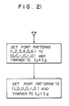
- Fig. 20 One example thereof is shown in Fig. 20.
- checking is made on if or not the value of ⁇ * is small in F6050. If it is small, a judgement that the time of the succeeding mode, i.e. the mode l-3 is short is made, and the turn-off/on processing to be performed during the succeeding mode l-3 is completed within the mode l-2. Therefore, the mode to be executed subsequently to the mode l-2 is the mode l-4 so that the jumping destination is set to the mode l-4 in F6090.
- the self-interruption is set not after T2 but after (T2 + T3) in F6l00, and a next interruption is awaited.
- the mode l-3 is executable since the ⁇ * is sufficiently large, the processing is performed in the sequence of F6060 and F6070, and the mode jumping is not made.
- the aforesaid processing of setting plural turn-off/on schedules in the same timer interruption interval permits the generation of a pulse having so short a pulse width that cannot be generated in the normal interruption processing, thereby extending the possibility of a harmonics reducing control.
- the aforesaid processing have been adapted to the flow from the mode l-2 to the modes l-3 and l-4 but may be also adapted to the other flows relative to the mode having a narrow width.
- This embodiment provides the following meritorious effects.
- the pulse generation in a power converter can be scheduled by a one-chip microcomputer.
- This permits a low harmonic, high reliability power coverter system to be constructed with low cost, and so permits an elevator to be controlled so that it can be operated with sufficiently low noise and low torque ripple.
Landscapes
- Engineering & Computer Science (AREA)
- Power Engineering (AREA)
- Inverter Devices (AREA)
- Rectifiers (AREA)
- Control Of Ac Motors In General (AREA)
- Ac-Ac Conversion (AREA)
- Power Conversion In General (AREA)
Applications Claiming Priority (2)
| Application Number | Priority Date | Filing Date | Title |
|---|---|---|---|
| JP2875/86 | 1986-01-11 | ||
| JP61002875A JPH0697854B2 (ja) | 1986-01-11 | 1986-01-11 | 電力変換装置の制御装置 |
Publications (3)
| Publication Number | Publication Date |
|---|---|
| EP0232702A2 true EP0232702A2 (de) | 1987-08-19 |
| EP0232702A3 EP0232702A3 (en) | 1989-03-08 |
| EP0232702B1 EP0232702B1 (de) | 1993-10-27 |
Family
ID=11541525
Family Applications (1)
| Application Number | Title | Priority Date | Filing Date |
|---|---|---|---|
| EP87100048A Expired - Lifetime EP0232702B1 (de) | 1986-01-11 | 1987-01-02 | Einrichtung und Verfahren zum Steuern eines Leistungskonverters |
Country Status (9)
| Country | Link |
|---|---|
| US (1) | US4870556A (de) |
| EP (1) | EP0232702B1 (de) |
| JP (1) | JPH0697854B2 (de) |
| KR (1) | KR950013238B1 (de) |
| CN (1) | CN1008866B (de) |
| CA (1) | CA1273115A (de) |
| DE (1) | DE3787899T2 (de) |
| HK (1) | HK59895A (de) |
| SG (1) | SG28374G (de) |
Cited By (3)
| Publication number | Priority date | Publication date | Assignee | Title |
|---|---|---|---|---|
| GB2229870A (en) * | 1989-03-13 | 1990-10-03 | Hitachi Ltd | A power converter with current-type inverter |
| EP0338798B1 (de) * | 1988-04-18 | 1994-07-13 | Daikin Industries, Limited | Pulsbreitenmodulierungssteuereinheit für Wechselrichter |
| RU2606401C2 (ru) * | 2011-03-21 | 2017-01-10 | Лабиналь Пауэр Системз | Упрощенный способ управления преобразователем трехфазного переменного напряжения в постоянное напряжение |
Families Citing this family (24)
| Publication number | Priority date | Publication date | Assignee | Title |
|---|---|---|---|---|
| JP2751170B2 (ja) * | 1987-12-26 | 1998-05-18 | 三菱電機株式会社 | インバータ装置の運転制御装置 |
| JPH0793823B2 (ja) * | 1988-02-01 | 1995-10-09 | 株式会社日立製作所 | 電圧形インバータのpwm制御装置 |
| US5256949A (en) * | 1989-05-23 | 1993-10-26 | Thor Technology Corporation | AC power line current regeneration |
| US4994950A (en) * | 1990-07-31 | 1991-02-19 | Eaton Corporation | Waveform generator for inverter control |
| US5168439A (en) * | 1990-11-27 | 1992-12-01 | General Electric Company | Inverter control method and apparatus |
| US5414615A (en) * | 1990-11-27 | 1995-05-09 | General Electric Company | Pattern generation control for inverter drives |
| IT1254734B (it) * | 1992-03-24 | 1995-10-10 | Faac Spa | Metodo e dispositivo per il controllo della velocita' di motori asincroni |
| US5400237A (en) * | 1992-05-11 | 1995-03-21 | Simmonds Precision Products, Inc. | PWM inverter controller with waveform memory |
| US5309349A (en) * | 1992-09-22 | 1994-05-03 | Industrial Technology Research Institute | Current detection method for DC to three-phase converters using a single DC sensor |
| US5687049A (en) * | 1996-01-26 | 1997-11-11 | International Rectifier Corporation | Method and circuit for protecting power circuits against short circuit and over current faults |
| FR2752111B1 (fr) * | 1996-07-30 | 1998-10-30 | Texas Instruments France | Procede et dispositif de commande d'onduleurs |
| JP3294236B2 (ja) * | 2000-06-16 | 2002-06-24 | 三菱重工業株式会社 | インバータ装置 |
| ES2255837B1 (es) * | 2004-10-05 | 2007-07-16 | Universidad De Alcala | Controlador electronico para convertidor de potencia, bidireccional, basado en dos inversores multinivel. |
| DE112004003035B4 (de) * | 2004-12-27 | 2018-02-08 | Danfoss Drives A/S | Verfahren zur Feststellung von Zuständen mit Erdschluss bei einer Motorsteuerung |
| JP4442593B2 (ja) * | 2006-07-20 | 2010-03-31 | 株式会社日立製作所 | 電力変換装置 |
| US7642666B2 (en) * | 2006-11-02 | 2010-01-05 | Hitachi, Ltd. | Wind power generation apparatus, wind power generation system and power system control apparatus |
| WO2008116467A2 (en) * | 2007-03-27 | 2008-10-02 | Danfoss Drives A/S | Method for driving a pulse width modulated controller |
| US8903577B2 (en) | 2009-10-30 | 2014-12-02 | Lsi Industries, Inc. | Traction system for electrically powered vehicles |
| US7598683B1 (en) | 2007-07-31 | 2009-10-06 | Lsi Industries, Inc. | Control of light intensity using pulses of a fixed duration and frequency |
| US8604709B2 (en) | 2007-07-31 | 2013-12-10 | Lsi Industries, Inc. | Methods and systems for controlling electrical power to DC loads |
| JP5214380B2 (ja) * | 2008-09-22 | 2013-06-19 | 株式会社日立プラントテクノロジー | クレーンのマトリックスコンバータの制御方法 |
| US20140169055A1 (en) * | 2012-12-18 | 2014-06-19 | Enphase Energy, Inc. | Non-isolated dc/ac inverter |
| US9385620B1 (en) * | 2013-01-10 | 2016-07-05 | Lockheed Martin Corporation | AC link converter switch engine |
| KR102088231B1 (ko) * | 2015-04-13 | 2020-03-13 | 엘에스산전 주식회사 | 인버터의 제어 장치 |
Family Cites Families (10)
| Publication number | Priority date | Publication date | Assignee | Title |
|---|---|---|---|---|
| US3905023A (en) * | 1973-08-15 | 1975-09-09 | Burroughs Corp | Large scale multi-level information processing system employing improved failsaft techniques |
| SU665379A1 (ru) * | 1975-06-05 | 1979-05-30 | Уральский ордена Трудового Красного Знамени политехнический институт им. С.М.Кирова | Статический преобразователь переменного тока в переменный |
| DE2829793A1 (de) * | 1978-07-06 | 1980-01-17 | Siemens Ag | Steuersatz fuer einen stromrichter |
| US4331994A (en) * | 1979-09-28 | 1982-05-25 | Borg-Warner Corporation | Shootthrough fault protection system for a voltage source transistor inverter |
| JPS5725171A (en) * | 1980-07-22 | 1982-02-09 | Meidensha Electric Mfg Co Ltd | Pulse width modulation type inverter |
| JPS6043757B2 (ja) * | 1981-05-06 | 1985-09-30 | 株式会社日立製作所 | 電動機の制御方法およびその制御装置 |
| US4475150A (en) * | 1982-04-28 | 1984-10-02 | General Electric Company | Coordinated load commutated inverter protection system |
| ZA837849B (en) * | 1982-11-03 | 1984-06-27 | Bbc Brown Boveri & Cie | Static power converter |
| JPS61102172A (ja) * | 1984-10-23 | 1986-05-20 | Hitachi Ltd | 自己消弧素子利用電流形コンバ−タ装置 |
| JPS61248881A (ja) * | 1985-04-22 | 1986-11-06 | 三菱電機株式会社 | エレベ−タの制御装置 |
-
1986
- 1986-01-11 JP JP61002875A patent/JPH0697854B2/ja not_active Expired - Fee Related
-
1987
- 1987-01-02 EP EP87100048A patent/EP0232702B1/de not_active Expired - Lifetime
- 1987-01-02 SG SG1995905774A patent/SG28374G/en unknown
- 1987-01-02 DE DE87100048T patent/DE3787899T2/de not_active Expired - Fee Related
- 1987-01-07 CA CA000526843A patent/CA1273115A/en not_active Expired - Lifetime
- 1987-01-08 KR KR1019870000085A patent/KR950013238B1/ko not_active Expired - Fee Related
- 1987-01-10 CN CN87100103A patent/CN1008866B/zh not_active Expired
- 1987-01-12 US US07/002,283 patent/US4870556A/en not_active Expired - Fee Related
-
1995
- 1995-04-20 HK HK59895A patent/HK59895A/en not_active IP Right Cessation
Cited By (4)
| Publication number | Priority date | Publication date | Assignee | Title |
|---|---|---|---|---|
| EP0338798B1 (de) * | 1988-04-18 | 1994-07-13 | Daikin Industries, Limited | Pulsbreitenmodulierungssteuereinheit für Wechselrichter |
| GB2229870A (en) * | 1989-03-13 | 1990-10-03 | Hitachi Ltd | A power converter with current-type inverter |
| GB2229870B (en) * | 1989-03-13 | 1993-10-20 | Hitachi Ltd | A power converter with current-type inverter |
| RU2606401C2 (ru) * | 2011-03-21 | 2017-01-10 | Лабиналь Пауэр Системз | Упрощенный способ управления преобразователем трехфазного переменного напряжения в постоянное напряжение |
Also Published As
| Publication number | Publication date |
|---|---|
| SG28374G (en) | 1995-09-01 |
| HK59895A (en) | 1995-04-28 |
| CN87100103A (zh) | 1987-11-04 |
| CA1273115A (en) | 1990-08-21 |
| US4870556A (en) | 1989-09-26 |
| JPH0697854B2 (ja) | 1994-11-30 |
| CN1008866B (zh) | 1990-07-18 |
| EP0232702B1 (de) | 1993-10-27 |
| KR950013238B1 (ko) | 1995-10-26 |
| EP0232702A3 (en) | 1989-03-08 |
| KR870007599A (ko) | 1987-08-20 |
| JPS62163579A (ja) | 1987-07-20 |
| DE3787899D1 (de) | 1993-12-02 |
| DE3787899T2 (de) | 1994-03-24 |
Similar Documents
| Publication | Publication Date | Title |
|---|---|---|
| EP0232702A2 (de) | Einrichtung und Verfahren zum Steuern eines Leistungskonverters | |
| EP0265867B1 (de) | Einrichtung für die Steuerung von Leistungskonvertern | |
| US4419615A (en) | Method of controlling pulse width modulated inverter for use in induction motor drive | |
| US4346434A (en) | Apparatus for controlling an electric motor | |
| US5349351A (en) | Analog-digital converting device | |
| US4954726A (en) | Switching an inverter with stored signal sequences | |
| EP0524398A2 (de) | Schaltkreis zur Kontrolle des Ausgangsstroms von parallel geschalteten pulsbreitenmodulierten Wechslerichtern | |
| US4924373A (en) | Apparatus and method for controlling switching elements in a PWN-controlled voltage source inverter | |
| EP0293869B1 (de) | Leistungswandlungseinrichtung | |
| CA1280463C (en) | Apparatus for controlling power transducers of the pulse width modulation (pwm) control type | |
| US11342878B1 (en) | Regenerative medium voltage drive (Cascaded H Bridge) with reduced number of sensors | |
| WO1990007225A1 (en) | Control for producing a low magnitude voltage at the output of a pwm inverter | |
| US4268900A (en) | Device for controlling a plurality of converters | |
| US4536835A (en) | Direct A.C. to A.C. converter controlled by a data processor | |
| JP3034895B2 (ja) | 電力変換器システム | |
| JP3194067B2 (ja) | Pwmパルス発生装置 | |
| JP2832606B2 (ja) | 電源回路の制御装置 | |
| JPH08228489A (ja) | 電力変換器の制御装置 | |
| KR910007043B1 (ko) | 교류전기차의 제어방식 | |
| JPH0714272B2 (ja) | 電力変換器の制御装置 | |
| JPH061982B2 (ja) | 電力変換装置 | |
| JPH06101932B2 (ja) | Pwm形コンバ−タの制御装置 | |
| SU987766A2 (ru) | Трехфазный инвертор | |
| SU1171929A1 (ru) | Устройство дл управлени многофазным преобразователем | |
| JPH0691751B2 (ja) | インバ−タの制御装置 |
Legal Events
| Date | Code | Title | Description |
|---|---|---|---|
| PUAI | Public reference made under article 153(3) epc to a published international application that has entered the european phase |
Free format text: ORIGINAL CODE: 0009012 |
|
| AK | Designated contracting states |
Kind code of ref document: A2 Designated state(s): CH DE FR GB IT LI NL SE |
|
| PUAL | Search report despatched |
Free format text: ORIGINAL CODE: 0009013 |
|
| AK | Designated contracting states |
Kind code of ref document: A3 Designated state(s): CH DE FR GB IT LI NL SE |
|
| 17P | Request for examination filed |
Effective date: 19890908 |
|
| 17Q | First examination report despatched |
Effective date: 19900103 |
|
| GRAA | (expected) grant |
Free format text: ORIGINAL CODE: 0009210 |
|
| AK | Designated contracting states |
Kind code of ref document: B1 Designated state(s): CH DE FR GB IT LI NL SE |
|
| REF | Corresponds to: |
Ref document number: 3787899 Country of ref document: DE Date of ref document: 19931202 |
|
| ITF | It: translation for a ep patent filed | ||
| ET | Fr: translation filed | ||
| PLBE | No opposition filed within time limit |
Free format text: ORIGINAL CODE: 0009261 |
|
| STAA | Information on the status of an ep patent application or granted ep patent |
Free format text: STATUS: NO OPPOSITION FILED WITHIN TIME LIMIT |
|
| 26N | No opposition filed | ||
| EAL | Se: european patent in force in sweden |
Ref document number: 87100048.5 |
|
| PGFP | Annual fee paid to national office [announced via postgrant information from national office to epo] |
Ref country code: FR Payment date: 19981215 Year of fee payment: 13 |
|
| PGFP | Annual fee paid to national office [announced via postgrant information from national office to epo] |
Ref country code: NL Payment date: 19981217 Year of fee payment: 13 |
|
| PGFP | Annual fee paid to national office [announced via postgrant information from national office to epo] |
Ref country code: SE Payment date: 19981221 Year of fee payment: 13 |
|
| PGFP | Annual fee paid to national office [announced via postgrant information from national office to epo] |
Ref country code: GB Payment date: 19981224 Year of fee payment: 13 |
|
| PGFP | Annual fee paid to national office [announced via postgrant information from national office to epo] |
Ref country code: CH Payment date: 19990119 Year of fee payment: 13 |
|
| PGFP | Annual fee paid to national office [announced via postgrant information from national office to epo] |
Ref country code: DE Payment date: 19990331 Year of fee payment: 13 |
|
| PG25 | Lapsed in a contracting state [announced via postgrant information from national office to epo] |
Ref country code: GB Free format text: LAPSE BECAUSE OF NON-PAYMENT OF DUE FEES Effective date: 20000102 |
|
| PG25 | Lapsed in a contracting state [announced via postgrant information from national office to epo] |
Ref country code: SE Free format text: LAPSE BECAUSE OF NON-PAYMENT OF DUE FEES Effective date: 20000103 |
|
| PG25 | Lapsed in a contracting state [announced via postgrant information from national office to epo] |
Ref country code: LI Free format text: LAPSE BECAUSE OF NON-PAYMENT OF DUE FEES Effective date: 20000131 Ref country code: CH Free format text: LAPSE BECAUSE OF NON-PAYMENT OF DUE FEES Effective date: 20000131 |
|
| PG25 | Lapsed in a contracting state [announced via postgrant information from national office to epo] |
Ref country code: NL Free format text: LAPSE BECAUSE OF NON-PAYMENT OF DUE FEES Effective date: 20000801 |
|
| GBPC | Gb: european patent ceased through non-payment of renewal fee |
Effective date: 20000102 |
|
| EUG | Se: european patent has lapsed |
Ref document number: 87100048.5 |
|
| REG | Reference to a national code |
Ref country code: CH Ref legal event code: PL |
|
| PG25 | Lapsed in a contracting state [announced via postgrant information from national office to epo] |
Ref country code: FR Free format text: LAPSE BECAUSE OF NON-PAYMENT OF DUE FEES Effective date: 20000929 |
|
| NLV4 | Nl: lapsed or anulled due to non-payment of the annual fee |
Effective date: 20000801 |
|
| PG25 | Lapsed in a contracting state [announced via postgrant information from national office to epo] |
Ref country code: DE Free format text: LAPSE BECAUSE OF NON-PAYMENT OF DUE FEES Effective date: 20001101 |
|
| REG | Reference to a national code |
Ref country code: FR Ref legal event code: ST |
|
| PG25 | Lapsed in a contracting state [announced via postgrant information from national office to epo] |
Ref country code: IT Free format text: LAPSE BECAUSE OF NON-PAYMENT OF DUE FEES;WARNING: LAPSES OF ITALIAN PATENTS WITH EFFECTIVE DATE BEFORE 2007 MAY HAVE OCCURRED AT ANY TIME BEFORE 2007. THE CORRECT EFFECTIVE DATE MAY BE DIFFERENT FROM THE ONE RECORDED. Effective date: 20050102 |