EP0226801B1 - Optical repeater and regulated current feeding system for the same - Google Patents
Optical repeater and regulated current feeding system for the same Download PDFInfo
- Publication number
- EP0226801B1 EP0226801B1 EP86115752A EP86115752A EP0226801B1 EP 0226801 B1 EP0226801 B1 EP 0226801B1 EP 86115752 A EP86115752 A EP 86115752A EP 86115752 A EP86115752 A EP 86115752A EP 0226801 B1 EP0226801 B1 EP 0226801B1
- Authority
- EP
- European Patent Office
- Prior art keywords
- current
- optical
- voltage
- conductor
- feeding
- Prior art date
- Legal status (The legal status is an assumption and is not a legal conclusion. Google has not performed a legal analysis and makes no representation as to the accuracy of the status listed.)
- Expired - Lifetime
Links
Images


Classifications
-
- H—ELECTRICITY
- H04—ELECTRIC COMMUNICATION TECHNIQUE
- H04B—TRANSMISSION
- H04B10/00—Transmission systems employing electromagnetic waves other than radio-waves, e.g. infrared, visible or ultraviolet light, or employing corpuscular radiation, e.g. quantum communication
- H04B10/80—Optical aspects relating to the use of optical transmission for specific applications, not provided for in groups H04B10/03 - H04B10/70, e.g. optical power feeding or optical transmission through water
- H04B10/806—Arrangements for feeding power
- H04B10/808—Electrical power feeding of an optical transmission system
Definitions
- the present invention relates to an optical communication system and more specifically to a power feeding system in which at least one optical repeater is provided in the optical communication path, a regulated current feeding equipment which supplies a constant DC current to each repeater is provided at the one end or both ends of the optical communication path and electronic power is supplied to each optical repeater from this regulated current feeding equipment through conductors.
- a power feeding system of the present invention is employed for an ordinary optical communication system and is also suitable for a power feeding system employed for an optical communication system having long transmitting or receiving distance, for example, the submarine optical communication system.
- Fig. 1 illustrates an ordinary DC power feeding system of the type known from JP-A-56-154 839.
- the n-repeaters 1 to n in total are connected in series to the power transmission path C1 and a constant current I is supplied to each repeater from the regulated current feeding equipments 1, 10 provided at both ends of power transmission path.
- the regulated current feeding equipments 1, 10 are provided at both ends because each power feeding equipment is destined to supply the power respectively to n/2-repeaters and thereby a load of one power feeding equipment can be alleviated, and this method is adapted for the system which provides a long transmission distance such as a submarine coaxial transmission system.
- Fig. 1 In case the transmission distance is short or each power feeding equipment has sufficient power and the one power feeding equipment fails in Fig. 1, power feeding is carried out by only one power feeding equipment.
- the DC power feeding system illustrated in Fig. 1 is also employed even in the optical fiber cable communication, particularly a submarine optical communication system.
- the power transmission path C1 in Fig. 1 is a conductor within the optical fiber cable.
- Fig. 2 illustrates detail of each repeater 1 to n in Fig. 1 and an optical repeater used in the optical communication system which is the object of the present invention.
- an optical repeater has a signal amplifier circuit 42 comprising a photoelectric conversion element, an amplifier circuit and a light emitting element, etc.
- a current I'' branched from the feeding current I' provided through the power transmission path C1 in order to supply the necessary power to the signal amplifier circuit 42 is supplied to said signal amplifier circuit 42 and a voltage V R obtained at both ends of zener diode 41' by applying other branched current I''' to the zener diode 41' is applied to the signal amplifier circuit 42.
- a power V R x I'' is supplied to the signal amplifying circuit 41'.
- C2 is the signal transmission path formed by optical fiber.
- a feeding current I' required for the optical repeater is about 1 to 2A. This value is remarkably larger than the current of 100 to 200 mA which is a feeding current for the coaxial cable. This is because the optical repeater requires a bias current and a drive current for an optical semi-conductor, such as laser diode, A.P.D., therefore larger current is consumed by these in comparison with the coaxial cable system.
- the power feeding equipment tends to be the same as that for dealing with a high voltage.
- a feeding voltage is about 5 kV, but in the optical communication system, it is expected to be about 15 kV for the power feeding equipment.
- selection or circuit elements becomes difficult and mounting of such circuit elements also becomes difficult.
- JP-A-56-154 839 describes a repeater circuit and DC power supply therefor, in an optical submarine communication system.
- a Zener diode is used in the power supply conductor to generate a fixed DC voltage when current flows therein.
- the output of the Zener diode is then converted to an AC voltage which is transformed by an isolating transformer to a lower AC voltage.
- the lower AC voltage is then rectified to a DC voltage and supplied to the repeater circuit.
- an optical repeater which is coupled between an optical transmission line, composed of optical fibers and a conductor comprising: an electrical circuit for converting input optical signals received from an input side of said optical fibers to electrical signals, for amplifying said electrical signals, for converting the amplified electrical signals to output optical signals, and for transmitting said output optical signals to an output side of said optical fibers, and a power supply means connected in series with said conductor for feeding primary regulated DC current from at least one terminal of said optical transmission line, for receiving said primary regulated DC current, for converting said primary regulated DC current into a secondary DC current, higher than said primary DC current and for supplying said secondary DC current to said electrical circuit, characterized by means for controlling said power supply means to generate a predetermined DC secondary voltage, and voltage detecting means for detecting the secondary DC voltage and said controlling means controlling said power supply means in accordance with the output of said voltage detecting means.
- Fig. 3 is a block diagram indicating an example of structure of the optical communication system to which the present invention is applied.
- an optical terminal A and terminal B are connected with optical fiber cables 3, 5, 6 and 8, and a plurality of optical repeaters 4, 7 are provided between such cables.
- the optical fiber cable is formed by the optical fiber C2 for transmitting optical information and a conductor (power trnsmission path) C1 which is a reinforcing material of the optical fiber and also operates as the power transmission path.
- the optical terminal devices 2, 9 are connected respectively at the terminal A and terminal B.
- regulated current feeding equipments, regulated current sources 1, 10 are provided at the terminals A, B of the conductor C1.
- the signal amplifier circuits 42, 72 and the current-fed switching type power supply circuits 41, 71 are provided at the optical repeaters 4, 7.
- the signal amplifier circuit 42 is similar to the existing one and comprises a light receiving element 421 which senses the optical signal from the optical fiber C2 i and converts it to an electrical signal, a transistor 422 which amplifies such signal sent from said light receiving element and a light emitting element 423 which receives the amplified signal and emits the light to the next optical fiber C2 o .
- the current-fed switching type voltage drop power supply circuit 41 supplies a necessary power to the signal amplifier circuit 42 and comprises transistors 411, 412, transformer T, rectifying diode D, capacitors Ca, Cb, voltage detection circuit 413 and pulse generating circuit 414.
- the primary side of transformer T is connected to the conductor C1 while the secondary side is used as the power supply of signal amplifier circuit 42 through the rectifying diode D.
- the transistor 411 converts a constant current into an AC voltage through repetition of ON and OFF states in accordance with the pulse frequency and pulse width given from the pulse generating circuit 414 and the transformer T drops the AC voltages obtained at both ends a, b of the primary side thereof.
- An AC current obtained at both ends c, d in the secondary side of transformer T is rectified by the diode D is regulated to a constant voltage by controlling the pulse width supplied to the transistor 411 and is supplied as the power to the signal amplifier circuit 42.
- the capacitors Ca and Cb are provided for smoothing.
- the voltage detection circuit 413 trigers the pulse generating circuit 414 when a DC voltage obtained between e and d is higher than the predetermined value causing it to generate the pulse of the predetermined width within the predetermined period. This pulse is applied to the base of transistor 411.
- the voltage detection circuit 413 makes constant a voltage between e and d by controlling the base of transistor 412.
- the current-fed switching type power supply circuit 71 has the structure similar to that of said current-fed switching type voltage drop power supply circuit 41 and provides the similar operations.
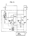
- Fig. 5 illustrates the second embodiment of the present invention.
- the current-fed switching type power supply circuit 41a according to the second embodiment of the present invention is formed with a switched capacitor circuit.
- Recent advances in ceramic technology has realized a high frequency switching type power supply circuit which does not use electrolytic capacitor and transformer as the switched capacitor circuit, but uses instead a hybrid IC or LSI utilizing a ceramic capacitor and ceramic substrate.
- the switched capacitor circuit with hybrid IC or LSI is used as the current-fed switching type power supply circuit.
- the switched capacitor circuit 41a comprises the switches SW1-1, SW1-2, SW2-1, SW2-2, ceramic capacitors Cc, Cd, Ce, rectifying diodes D1 D2, D3, D4, voltage detection circuit 501 and pulse generating circuit 502.
- the voltage detection circuit 501 detects an input voltage or the signal amplifying circuit (same as that illustrated in Fig. 4) and triggers the pulse generating circuit 502 in accordance with its input voltage.
- the pulse generating circuit 502 outputs the complementary two pulses P1, P2 having the period and pulse width depending on the output signal of voltage detection circuit 501.
- the pulse P1 controls the switches SW1-1, SW1-2, while the pulse P2 the switches SW2-1, SW2-2. When the switches SW1-1, SW1-2 are ON the switches SW2-1, SW2-2 are OFF. When the switches SW1-1, SW1-2 are OFF, the switches SW2-1, SW2-2 are ON.
- This second embodiment provides excellent effect that long operation life can be assured because a ceramic capacitor is used in place of the electrolytic capacitor and easy mounting is also realized because it is formed as the hybrid IC.
- FIG. 6 An equivalent of the optical communication system comprising the current-fed switching type power supply circuit 41 or 41a considered from the viewpoint of power consumption is illustrated in Fig. 6.
- R c1 , R c2 , ...., R cn are resistances of conductor within the optical fiber cable and R R is equivalent value of power consumption P R within each optical repeater as a resistance.
- This power consumption P R is set to constant for all optical repeaters.
- Fig. 7 indicates such relation.
- the power consumption P R is constant because it does not depend on a feeding current.
- Power loss Pc of coductor is proportional to the square of feeding current.
- a supply voltage V depends on the feeding current and has the property illustrated in Fig. 7.
- a feeding voltage V can be minimized when the power consumption of repeater is equal to that of conductor.
- it is better to reduce a feeding current as much as possible.
- a feeding current is set considering such problem.
- total power is 1.25 kW, which is about 1/3 or less of the existing system.
- the feeding voltage is also 2.5 kV which is equal to that of above case.
- power loss of conductor becomes 0.04 kW which is about 1/4 of the total power of existing system.
- a feeding voltage is 5.2 kV and it does not result in any problem from the viewpoint of high voltage.
- the current-fed switching type power supply circuit being put into practical use assures the conversion efficiency of 80% or more.
- the power loss of such power supply circuit is assumed as 20%, power loss of each repeater becomes 48W and total power becomes 1.45 kW. Therefore, even when considering loss of power supply circuit provided to each repeater, the total power consumption can be suppressed sufficiently in comparison with that of the existing system.
- the optimum feeding current can be set considering factors sch as communication distance and power consumption of repeaters, etc. under the condition that power consumption is minimized and increase of feeding voltage is limited to a certain degree.
- the present invention can remarkably save power consumption of the optical communication system and reduce the size of power feeding equipment by decreasing a feeding current.
Landscapes
- Physics & Mathematics (AREA)
- Electromagnetism (AREA)
- Engineering & Computer Science (AREA)
- Computer Networks & Wireless Communication (AREA)
- Signal Processing (AREA)
- Optical Communication System (AREA)
- Cable Transmission Systems, Equalization Of Radio And Reduction Of Echo (AREA)
- Transmitters (AREA)
Applications Claiming Priority (2)
| Application Number | Priority Date | Filing Date | Title |
|---|---|---|---|
| JP60262461A JPS62123842A (ja) | 1985-11-25 | 1985-11-25 | 光通信装置 |
| JP262461/85 | 1985-11-25 |
Publications (3)
| Publication Number | Publication Date |
|---|---|
| EP0226801A2 EP0226801A2 (en) | 1987-07-01 |
| EP0226801A3 EP0226801A3 (en) | 1989-02-01 |
| EP0226801B1 true EP0226801B1 (en) | 1994-07-13 |
Family
ID=17376104
Family Applications (1)
| Application Number | Title | Priority Date | Filing Date |
|---|---|---|---|
| EP86115752A Expired - Lifetime EP0226801B1 (en) | 1985-11-25 | 1986-11-13 | Optical repeater and regulated current feeding system for the same |
Country Status (5)
| Country | Link |
|---|---|
| US (1) | US4879762A (enExample) |
| EP (1) | EP0226801B1 (enExample) |
| JP (1) | JPS62123842A (enExample) |
| CA (1) | CA1249342A (enExample) |
| DE (1) | DE3689970T2 (enExample) |
Families Citing this family (16)
| Publication number | Priority date | Publication date | Assignee | Title |
|---|---|---|---|---|
| DE3808892C2 (de) * | 1988-03-17 | 1997-04-30 | Sel Alcatel Ag | Verstärker für Licht |
| JPH04217123A (ja) * | 1990-12-18 | 1992-08-07 | Fujitsu Ltd | 光伝送システムの給電方式 |
| JPH05122159A (ja) * | 1991-05-13 | 1993-05-18 | Internatl Business Mach Corp <Ibm> | 伝送信号の信号対雑音比の改良方法及び光学的相互接続システム |
| US5777769A (en) * | 1995-12-28 | 1998-07-07 | Lucent Technologies Inc. | Device and method for providing high speed data transfer through a drop line of a power line carrier communication system |
| GB9604427D0 (en) * | 1996-03-01 | 1996-05-01 | Stc Submarine Systems Ltd | A branching unit |
| DE19637417B4 (de) * | 1996-09-13 | 2008-08-14 | Bayerische Motoren Werke Aktiengesellschaft | Betriebsverfahren für einen Datenbus |
| US5945668A (en) * | 1997-06-20 | 1999-08-31 | Sun Microsystems, Inc. | Fiber optic system with open fiber safety interlock |
| DE19833613A1 (de) | 1998-07-25 | 2000-01-27 | Bayerische Motoren Werke Ag | Optischer Datenbus für ein Fahrzeug |
| US7233744B1 (en) * | 1999-10-07 | 2007-06-19 | Tyco Telecommunications (Us) Inc. | Power feed arrangement using aggregate segments |
| US20030059156A1 (en) * | 2001-09-24 | 2003-03-27 | Feinberg Lee Daniel | Bifurcated optical and power connectivity for ultra long-haul optical communication systems |
| US20030108351A1 (en) * | 2001-09-24 | 2003-06-12 | Feinberg Lee Daniel | Methods for ultra long-haul optical communications |
| US6838865B2 (en) * | 2003-05-14 | 2005-01-04 | Northrop Grumman Corporation | Method and apparatus for branching a single wire power distribution system |
| EP2270967B1 (en) | 2009-06-30 | 2019-03-13 | Alcatel Lucent | System and method for providing electric power to a submerged load |
| GB2533160A (en) * | 2014-12-12 | 2016-06-15 | Ge Oil & Gas Uk Ltd | Repeaters |
| US11223427B2 (en) * | 2017-03-17 | 2022-01-11 | Nec Corporation | Optical submarine cable system and optical submarine relay apparatus |
| FR3078217B1 (fr) * | 2018-02-21 | 2020-03-13 | Alstom Transport Technologies | Procede d'echange de donnees dans un equipement electronique, equipement electronique, vehicule ferroviaire et installation ferroviaire associes |
Citations (1)
| Publication number | Priority date | Publication date | Assignee | Title |
|---|---|---|---|---|
| JPS56154839A (en) * | 1980-05-01 | 1981-11-30 | Fujitsu Ltd | Power feeding circuit of optical submarine repeater |
Family Cites Families (6)
| Publication number | Priority date | Publication date | Assignee | Title |
|---|---|---|---|---|
| JPS5172220A (enExample) * | 1974-12-20 | 1976-06-22 | Hitachi Ltd | |
| US4255782A (en) * | 1977-11-15 | 1981-03-10 | Jgf, Incorporated | Electrical energy conversion systems |
| JPS58187015A (ja) * | 1982-04-26 | 1983-11-01 | Nippon Telegr & Teleph Corp <Ntt> | スイツチト・キヤパシタ回路 |
| US4419812A (en) * | 1982-08-23 | 1983-12-13 | Ncr Corporation | Method of fabricating an integrated circuit voltage multiplier containing a parallel plate capacitor |
| DE3330045A1 (de) * | 1983-08-19 | 1985-03-07 | Siemens AG, 1000 Berlin und 8000 München | Schaltungsanordnung zur speisung von elektrischen gleichstromverbraucheranordnungen |
| US4654769A (en) * | 1984-11-02 | 1987-03-31 | California Institute Of Technology | Transformerless dc-to-dc converters with large conversion ratios |
-
1985
- 1985-11-25 JP JP60262461A patent/JPS62123842A/ja active Granted
-
1986
- 1986-11-13 EP EP86115752A patent/EP0226801B1/en not_active Expired - Lifetime
- 1986-11-13 DE DE3689970T patent/DE3689970T2/de not_active Expired - Fee Related
- 1986-11-21 US US06/933,114 patent/US4879762A/en not_active Expired - Fee Related
- 1986-11-24 CA CA000523628A patent/CA1249342A/en not_active Expired
Patent Citations (1)
| Publication number | Priority date | Publication date | Assignee | Title |
|---|---|---|---|---|
| JPS56154839A (en) * | 1980-05-01 | 1981-11-30 | Fujitsu Ltd | Power feeding circuit of optical submarine repeater |
Also Published As
| Publication number | Publication date |
|---|---|
| DE3689970D1 (de) | 1994-08-18 |
| EP0226801A3 (en) | 1989-02-01 |
| EP0226801A2 (en) | 1987-07-01 |
| DE3689970T2 (de) | 1994-12-08 |
| CA1249342A (en) | 1989-01-24 |
| US4879762A (en) | 1989-11-07 |
| JPH0420538B2 (enExample) | 1992-04-03 |
| JPS62123842A (ja) | 1987-06-05 |
Similar Documents
| Publication | Publication Date | Title |
|---|---|---|
| EP0226801B1 (en) | Optical repeater and regulated current feeding system for the same | |
| US4809151A (en) | Switching regulator having parallel diode isolated primary windings and plural secondary windings | |
| US5963438A (en) | Bi-directional magnetic isolator | |
| EP1459430A2 (en) | A power converter | |
| EP0792007A3 (en) | Universal power module | |
| US7015702B2 (en) | Method for evaluating a measuring signal and corresponding circuit arrangement | |
| JPH07131426A (ja) | 光パワー変換回路 | |
| EP0749227A2 (en) | Transmission using pulse position coding | |
| JPH1189120A (ja) | 光パワー伝送方法及び装置 | |
| JPH1189113A (ja) | 無停電電源装置 | |
| JPH11150492A (ja) | 海底ケーブルシステム用電源回路 | |
| JPH06141536A (ja) | Dc/dcコンバータを含む低損失電源供給装置 | |
| US6865095B2 (en) | Power circuit | |
| US6633493B2 (en) | Inherently short-circuit resistant power distribution system | |
| CA2263918A1 (en) | Voltage conversion circuit for a laser based distance measurement and ranging | |
| EP0366044B1 (en) | Data communications system | |
| NL2037352B1 (en) | power converter system | |
| JP7521610B2 (ja) | 電源回路及び光海底ケーブル | |
| US20050185431A1 (en) | DC/DC converter | |
| US6462970B2 (en) | SMPS protection circuit in electronic appliance | |
| SU1317592A1 (ru) | Многоканальный источник питани | |
| SU1352595A1 (ru) | Преобразователь посто нного напр жени | |
| JPS60249444A (ja) | 光通信装置 | |
| KR20210135412A (ko) | 신호 절연 전송장치 및 방법 | |
| JP2000059191A (ja) | 半導体スイッチ |
Legal Events
| Date | Code | Title | Description |
|---|---|---|---|
| PUAI | Public reference made under article 153(3) epc to a published international application that has entered the european phase |
Free format text: ORIGINAL CODE: 0009012 |
|
| AK | Designated contracting states |
Kind code of ref document: A2 Designated state(s): DE FR GB |
|
| PUAL | Search report despatched |
Free format text: ORIGINAL CODE: 0009013 |
|
| AK | Designated contracting states |
Kind code of ref document: A3 Designated state(s): DE FR GB |
|
| 17P | Request for examination filed |
Effective date: 19890403 |
|
| 17Q | First examination report despatched |
Effective date: 19910411 |
|
| GRAA | (expected) grant |
Free format text: ORIGINAL CODE: 0009210 |
|
| AK | Designated contracting states |
Kind code of ref document: B1 Designated state(s): DE FR GB |
|
| REF | Corresponds to: |
Ref document number: 3689970 Country of ref document: DE Date of ref document: 19940818 |
|
| ET | Fr: translation filed | ||
| PLBE | No opposition filed within time limit |
Free format text: ORIGINAL CODE: 0009261 |
|
| STAA | Information on the status of an ep patent application or granted ep patent |
Free format text: STATUS: NO OPPOSITION FILED WITHIN TIME LIMIT |
|
| 26N | No opposition filed | ||
| PGFP | Annual fee paid to national office [announced via postgrant information from national office to epo] |
Ref country code: FR Payment date: 19991109 Year of fee payment: 14 |
|
| PGFP | Annual fee paid to national office [announced via postgrant information from national office to epo] |
Ref country code: GB Payment date: 19991110 Year of fee payment: 14 |
|
| PGFP | Annual fee paid to national office [announced via postgrant information from national office to epo] |
Ref country code: DE Payment date: 19991115 Year of fee payment: 14 |
|
| PG25 | Lapsed in a contracting state [announced via postgrant information from national office to epo] |
Ref country code: GB Free format text: LAPSE BECAUSE OF NON-PAYMENT OF DUE FEES Effective date: 20001113 |
|
| GBPC | Gb: european patent ceased through non-payment of renewal fee |
Effective date: 20001113 |
|
| PG25 | Lapsed in a contracting state [announced via postgrant information from national office to epo] |
Ref country code: FR Free format text: LAPSE BECAUSE OF NON-PAYMENT OF DUE FEES Effective date: 20010731 |
|
| PG25 | Lapsed in a contracting state [announced via postgrant information from national office to epo] |
Ref country code: DE Free format text: LAPSE BECAUSE OF NON-PAYMENT OF DUE FEES Effective date: 20010801 |
|
| REG | Reference to a national code |
Ref country code: FR Ref legal event code: ST |