US4879762A - Optical repeater and regulated current feeding system for the same - Google Patents
Optical repeater and regulated current feeding system for the same Download PDFInfo
- Publication number
- US4879762A US4879762A US06/933,114 US93311486A US4879762A US 4879762 A US4879762 A US 4879762A US 93311486 A US93311486 A US 93311486A US 4879762 A US4879762 A US 4879762A
- Authority
- US
- United States
- Prior art keywords
- signal
- current
- optical
- regulated
- voltage
- Prior art date
- Legal status (The legal status is an assumption and is not a legal conclusion. Google has not performed a legal analysis and makes no representation as to the accuracy of the status listed.)
- Expired - Fee Related
Links
Images


Classifications
-
- H—ELECTRICITY
- H04—ELECTRIC COMMUNICATION TECHNIQUE
- H04B—TRANSMISSION
- H04B10/00—Transmission systems employing electromagnetic waves other than radio-waves, e.g. infrared, visible or ultraviolet light, or employing corpuscular radiation, e.g. quantum communication
- H04B10/80—Optical aspects relating to the use of optical transmission for specific applications, not provided for in groups H04B10/03 - H04B10/70, e.g. optical power feeding or optical transmission through water
- H04B10/806—Arrangements for feeding power
- H04B10/808—Electrical power feeding of an optical transmission system
Definitions
- the present invention relates to an optical communications system and more specifically to a power supply system used in an optical communications system in which at least one optical repeater is provided in an optical communications path; a regulated DC current source, which supplies a constant DC current to each repeater, is provided at one or both ends of the optical communications path; and power is supplied to each optical repeater from the DC current source through conductors.
- a power supply system according to the present invention can be employed in an ordinary optical communications system and is also suitable for use in an optical communications system having a long transmitting or receiving distance requirement, for example, an underwater optical communication system.
- AC power is supplied to the repeaters, rectifying and smoothing circuits must be provided for the repeaters, resulting in a complicated circuit.
- An advantage of using AC power is that a simple transformer can be employed to supply the AC voltage.
- This power supply method is often employed in transmission systems utilizing electron tube type repeaters, which require various voltage values to function. However, the power factor is lowered by the capacitance and inductance of the transmission cables used and, therefore, the voltage drop is high, reducing the power transmission efficiency (power required for all repeaters ⁇ power transmitted).
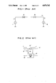
- FIG. 1 illustrates an ordinary DC power supply system for a communication system.
- the n-repeaters, 1 through n respectively, are connected in series to the power supply path C1, and a constant current I is supplied to each repeater from the regulated current supply equipment 1 and 10, respectively provided at the end of the power transmission path.
- the regulated current supply equipment 1 and 10 is provided at both ends because each power supply provides power to n/2 repeaters and, as a result, the load on the power supplies is reduced.
- This method is used for a system which has a long transmission distance requirement, such as an underwater coaxial communication system. If the transmission distance is short, or if each power supply in FIG. 1 has a sufficient power rating and one of the power supplies fails, power can be supplied by only one power supply.
- the DC power supply system illustrated in FIG. 1 can also be employed in an optical fiber cable communication system, including an underwater optical communication system.
- FIG. 2 illustrates an optical repeater used in an existing optical communication system.
- an optical repeater has a signal amplifier circuit 42 comprising a photoelectric conversion element, an amplifier circuit and a light-emitting element.
- a current I" is drawn from the supply current I' provided through the power supply path Cl, in order to supply the necessary power to the signal amplifier circuit 42.
- a voltage V R across zener diode 41' obtained by applying current I'" to the zener diode 41', is also supplied to the signal amplifier circuit 42.
- a power V R ⁇ I" is supplied to the signal amplifying circuit 42.
- C2 is a signal transmission path formed by an optical fiber.
- optical repeater 2 is formed by a zener diode and has the advantage that it is small and reliable, but it also has the disadvantage that it raises the supply current requirement of the optical repeater to about 1 to 2A. This value is quite a bit larger than the supply current requirement for a coaxial cable system, which is 100 to 200mA.
- the difference in requirements is due to the fact that an optical repeater requires a bias current and a drive current for an optical semiconductor, such as a laser diode or an avalanche photodiode, and therefore a larger amount of current is consumed by an optical repeater system in comparison to a coaxial cable system.
- the power supply equipment in a conventional optical communication system must be considerably large in size in order to compensate for the power consumption in the power transmission path C1. This is particularly true in a long range transmission system such as an underwater optical communication system.
- This large power consumption by the power transmission path C1 is a serious problem from an economic standpoint.
- a supply voltage of approximately 5kV is required, but in a conventional optical communication system, a supply voltage of approximately 15kV is required.
- the selection of circuit elements and mounting of such circuit elements becomes difficult and expensive.
- an optical repeater is coupled between an optical transmission line composed of optical fibers and a conductor, the repeater comprising an electrical circuit for converting input optical signals, received from the input side of said optical transmission line, to electrical signals, for amplifying said electrical signals, for converting the amplified electrical signals to output optical signals, and for transmitting said output optical signals to the output side of said optical transmission line; and a power supply circuit connected in series with said conductor for receiving regulated DC current from at least one terminal of said optical transmission line, for receiving said regulated DC current, for dropping the received voltage of said regulated DC current, and for supplying higher DC current than said regulated DC current to said electrical circuit.
- FIG. 1 is a circuit drawing of an existing regulated current feeding system in a wired transmission system
- FIG. 2 is a block diagram of an optical repeater used in an existing system for optical communication
- FIG. 3 is a block diagram of an optical communication system to which the regulated current feeding system for optical communication of the present invention is applied;
- FIG. 4 is a circuit diagram of an optical repeater according to the present invention.
- FIG. 5 is a circuit diagram of an optical repeater of another embodiment of the present invention.
- FIG. 6 is a circuit diagram of an equivalent circuit of FIG. 3;
- FIG. 7 is a graph showing characteristic curves indicating power consumption of an optical repeater and power transmission path in a regulated current feeding system according to the invention.
- FIG. 3 is a block diagram of an example of an optical communication system to which the present invention can be applied.
- an optical terminal A and terminal B are connected with optical fiber cables 3, 5, 6 and 8, and a plurality of optical repeaters 4, 7 are provided between such cables.
- the optical fiber cables are formed by the optical fiber C2, for transmitting optical information, and a conductor (power supply path) C1 for supplying power to the optical repeaters.
- the optical terminal devices 2 and 9 are connected to optical fiber C2 at terminal A and terminal B, respectively.
- Regulated current sources 1 and 10 are coupled to conductor C1 at terminals A and B, respectively.
- the signal amplifier circuits 42, 72 and current-fed switching type power supply circuits 41, 71 are provided within the optical repeaters 4, 7.
- the signal amplifier circuit 42 comprises: a light receiving element 421, which senses the optical signal from the optical fiber C2 i and converts it to an electrical signal; a transistor 422, which amplifies the signal sent from the light receiving element; and a light emitting element 423, which receives the amplified signal and emits the light to the next optical fiber C2 o .
- the current-fed switching type voltage-drop power supply circuit 41 supplies power to the signal amplifier circuit 42 and comprises transistors 411 and 412, step-down transformer T, rectifying diode D, capacitors Ca and Cb, voltage detection circuit 413, and pulse generating circuit 414.
- the primary side of transformer T is connected to the conductor C1, and the secondary side supplies power to signal amplifier circuit 42, through the rectifying diode D.
- the transistor 411 converts a constant current into an AC voltage by alternately switching between an ON and an OFF state, in accordance with the pulse frequency and pulse width supplied from the pulse generating circuit 414, and the transformer T steps down the AC voltage supplied across the primary side thereof.
- An AC current obtained across the secondary side of transformer T is rectified by the diode D, regulated to a constant voltage by controlling the pulse width supplied to the transistor 412, and is supplied to the signal amplifier circuit 42.
- the capacitors Ca and Cb are provided for smoothing.
- the voltage detection circuit 413 triggers the pulse generating circuit 414 when a DC voltage measured across terminals e and d is higher than a predetermined value, causing it to generate a pulse of a predetermined width and a predetermined frequency. This pulse is applied to the base of transistor 411.
- the voltage detection circuit 413 makes the voltage across terminals e and d constant by controlling the base of transistor 412.
- a current I 1 flowing through the secondary side is higher than the current I supplied to the primary side of transformer T from the regulated current source 1.
- the power supplied to the primary side of transformer T is substantially equal to the power obtained at the secondary side. Therefore, a current lower than the current required for driving the signal amplifier circuit 42 can be supplied by the regulated current sources 1 and 10.
- the voltage supplied to the signal amplifier circuit 42 is obtained from the current-fed switching type power supply circuit 41, utilizing a supply current I as described above, the voltage drop in conductor C1 of a regulated current I is lowered comparatively. Therefore, the difficulty of selection and mounting of circuit parts of the prior art, due to a high voltage requirement, is solved.
- FIG. 5 illustrates a second embodiment of the present invention.
- the current-fed switching type power supply circuit 41a is formed by a switched capacitor circuit.
- Recent advances in ceramic technology have led to the development of a high frequency switching type power supply circuit which does not require the use of an electrolytic capacitor and a transformer to form a switched capacitor circuit in a hybrid IC or LSI, but instead utilizes a ceramic capacitor and ceramic substrate.
- this new high frequency switching type power supply is used as the power supply circuit to provide power to the signal amplifier 42.
- the switched capacitor circuit 41a comprises switches SW1-1, SW1-2, SW2-1, SW2-2; ceramic capacitors Cc, Cd, Ce; rectifying diodes D1, D2, D3, D4; voltage detection circuit 501, and pulse generating circuit 502.
- the voltage detection circuit 501 detects an input voltage from the signal amplifying circuit 42 (same as that illustrated in FIG. 4) and triggers the pulse generating circuit 502 in accordance with the input voltage.
- the pulse generating circuit 502 outputs two complementary pulses P1, P2 having a period and pulse width which depend on the output signal of voltage detection circuit 501.
- the pulse P1 controls the switches SW1-1, SW1-2, while the pulse P2 controls the switches SW2-1, SW2-2.
- a voltage which is lower than the charging voltage across the capacitors Cc and Cd or Cd and Ce can be attained by selection of the period and pulse width of the two pulses P1, P2 output from the pulse generating circuit 502 and the capacitance values of the capacitors Cc, Cd and Ce.
- This voltage is applied to the signal amplifier circuit 42.
- a current which is lower than that required for driving the signal amplifier circuit 42 can be supplied from the regulated current source 1.
- This embodiment provides a long operating life because a ceramic capacitor is used in place of the electrolytic capacitor, and easy mounting is also possible because it is formed as a hybrid IC.
- FIG. 6 shows an equivalent circuit of FIG. 3 utilizing the current-fed switching type power supply circuit 41 or 41a, considered from the viewpoint of power consumption.
- R c1 , R c2 , . . . , R cn represent the resistance of the conductor C within the optical fiber cable
- R R represents the impedance of each optical repeater.
- the supply voltage V can be minimized when the power consumption of the repeater is equal to that of the conductor. On the other hand, from the point of view of minimizing total power consumption, it is better to reduce the supply current as much as possible. However, if it is greatly reduced, the operation of the current-fed switching type power supply circuit is affected, and there is also an increase of the supply voltage requirement. Therefore, the supply current must be selected with these two factors in mind.
- the power consumption of each optical repeater is 40W
- the resistance value of the conductor is 1 ohm/km
- the transmission path, of 1000 km in length is connected through 25 repeaters.
- the supply current is 2A
- the total power consumption of the repeaters is 1 kW
- the power consumption of the conductor is 4 kW. Therefore, a total of 5 kW is required as the supply power.
- the supply voltage is 2.5 kV.
- the power consumption of the conductor is lowered to 0.25 kW and the total power consumption of the repeaters is equal to 1 kW.
- the total supply power required is 1.25 kW, which is about 1/3 of that required by the conventional system.
- the feeding voltage is 2.5 kV, which is equal to that of conventional system.
- the power consumption of the conductor becomes 0.04 kW, which is about 1/4 of the total power consumed by the conventional system.
- the supply voltage is increased, but remains at a relatively low value of approximately 5.2 kV.
- the current-fed switching type power supply circuits presently being used have an efficiency of 80% or more. Assuming the loss of such a power supply circuit to be 20%, the power consumed by each repeater becomes 48W and total power becomes 1.45 kW. Therefore, even when considering the loss of the power supply circuit provided to each repeater, the total power consumption can still be lowered substantially in comparison to that of the existing system.
- the optimum supply current can be chosen considering factors such as the communication distance and the power consumption of the repeaters, etc. so that the power consumption is minimized and the increase of the supply voltage is limited to a certain degree.
- the present invention lowers the power consumption of optical communication systems and reduces the size of power supply equipment by decreasing the required supply current.
Landscapes
- Physics & Mathematics (AREA)
- Electromagnetism (AREA)
- Engineering & Computer Science (AREA)
- Computer Networks & Wireless Communication (AREA)
- Signal Processing (AREA)
- Optical Communication System (AREA)
- Cable Transmission Systems, Equalization Of Radio And Reduction Of Echo (AREA)
- Transmitters (AREA)
Applications Claiming Priority (2)
| Application Number | Priority Date | Filing Date | Title |
|---|---|---|---|
| JP60-262461 | 1985-11-25 | ||
| JP60262461A JPS62123842A (ja) | 1985-11-25 | 1985-11-25 | 光通信装置 |
Publications (1)
| Publication Number | Publication Date |
|---|---|
| US4879762A true US4879762A (en) | 1989-11-07 |
Family
ID=17376104
Family Applications (1)
| Application Number | Title | Priority Date | Filing Date |
|---|---|---|---|
| US06/933,114 Expired - Fee Related US4879762A (en) | 1985-11-25 | 1986-11-21 | Optical repeater and regulated current feeding system for the same |
Country Status (5)
| Country | Link |
|---|---|
| US (1) | US4879762A (enExample) |
| EP (1) | EP0226801B1 (enExample) |
| JP (1) | JPS62123842A (enExample) |
| CA (1) | CA1249342A (enExample) |
| DE (1) | DE3689970T2 (enExample) |
Cited By (13)
| Publication number | Priority date | Publication date | Assignee | Title |
|---|---|---|---|---|
| US5357363A (en) * | 1991-05-13 | 1994-10-18 | International Business Machines Corporation | Interconnections having improved signal-to-noise ratio |
| US5719693A (en) * | 1990-12-18 | 1998-02-17 | Fujitsu Limited | Power feeding system for an optical transmission system |
| DE19637417A1 (de) * | 1996-09-13 | 1998-03-19 | Bayerische Motoren Werke Ag | Betriebsverfahren für einen Datenbus |
| US5777769A (en) * | 1995-12-28 | 1998-07-07 | Lucent Technologies Inc. | Device and method for providing high speed data transfer through a drop line of a power line carrier communication system |
| US6005996A (en) * | 1996-03-01 | 1999-12-21 | Alcatel | Branching unit for an optical fiber transmission system |
| US6501577B1 (en) | 1998-07-25 | 2002-12-31 | Bayerische Motoren Werke Aktiengesellschaft | Optical data bus for a vehicle |
| US20030059156A1 (en) * | 2001-09-24 | 2003-03-27 | Feinberg Lee Daniel | Bifurcated optical and power connectivity for ultra long-haul optical communication systems |
| US20030108351A1 (en) * | 2001-09-24 | 2003-06-12 | Feinberg Lee Daniel | Methods for ultra long-haul optical communications |
| EP0886395A3 (en) * | 1997-06-20 | 2004-02-04 | Sun Microsystems, Inc. | Open fiber safety interlock |
| US7233744B1 (en) * | 1999-10-07 | 2007-06-19 | Tyco Telecommunications (Us) Inc. | Power feed arrangement using aggregate segments |
| WO2016091635A1 (en) * | 2014-12-12 | 2016-06-16 | Ge Oil & Gas Uk Limited | Repeaters |
| FR3078217A1 (fr) * | 2018-02-21 | 2019-08-23 | Alstom Transport Technologies | Procede d'echange de donnees dans un equipement electronique, equipement electronique, vehicule ferroviaire et installation ferroviaire associes |
| US20200059303A1 (en) * | 2017-03-17 | 2020-02-20 | Nec Corporation | Optical submarine cable system and optical submarine relay apparatus |
Families Citing this family (3)
| Publication number | Priority date | Publication date | Assignee | Title |
|---|---|---|---|---|
| DE3808892C2 (de) * | 1988-03-17 | 1997-04-30 | Sel Alcatel Ag | Verstärker für Licht |
| US6838865B2 (en) * | 2003-05-14 | 2005-01-04 | Northrop Grumman Corporation | Method and apparatus for branching a single wire power distribution system |
| EP2270967B1 (en) | 2009-06-30 | 2019-03-13 | Alcatel Lucent | System and method for providing electric power to a submerged load |
Citations (4)
| Publication number | Priority date | Publication date | Assignee | Title |
|---|---|---|---|---|
| US4255782A (en) * | 1977-11-15 | 1981-03-10 | Jgf, Incorporated | Electrical energy conversion systems |
| JPS56154839A (en) * | 1980-05-01 | 1981-11-30 | Fujitsu Ltd | Power feeding circuit of optical submarine repeater |
| US4622480A (en) * | 1982-04-26 | 1986-11-11 | Nippon Telegraph & Telephone Public Corporation | Switched capacitor circuit with high power supply projection ratio |
| US4654769A (en) * | 1984-11-02 | 1987-03-31 | California Institute Of Technology | Transformerless dc-to-dc converters with large conversion ratios |
Family Cites Families (3)
| Publication number | Priority date | Publication date | Assignee | Title |
|---|---|---|---|---|
| JPS5172220A (enExample) * | 1974-12-20 | 1976-06-22 | Hitachi Ltd | |
| US4419812A (en) * | 1982-08-23 | 1983-12-13 | Ncr Corporation | Method of fabricating an integrated circuit voltage multiplier containing a parallel plate capacitor |
| DE3330045A1 (de) * | 1983-08-19 | 1985-03-07 | Siemens AG, 1000 Berlin und 8000 München | Schaltungsanordnung zur speisung von elektrischen gleichstromverbraucheranordnungen |
-
1985
- 1985-11-25 JP JP60262461A patent/JPS62123842A/ja active Granted
-
1986
- 1986-11-13 EP EP86115752A patent/EP0226801B1/en not_active Expired - Lifetime
- 1986-11-13 DE DE3689970T patent/DE3689970T2/de not_active Expired - Fee Related
- 1986-11-21 US US06/933,114 patent/US4879762A/en not_active Expired - Fee Related
- 1986-11-24 CA CA000523628A patent/CA1249342A/en not_active Expired
Patent Citations (4)
| Publication number | Priority date | Publication date | Assignee | Title |
|---|---|---|---|---|
| US4255782A (en) * | 1977-11-15 | 1981-03-10 | Jgf, Incorporated | Electrical energy conversion systems |
| JPS56154839A (en) * | 1980-05-01 | 1981-11-30 | Fujitsu Ltd | Power feeding circuit of optical submarine repeater |
| US4622480A (en) * | 1982-04-26 | 1986-11-11 | Nippon Telegraph & Telephone Public Corporation | Switched capacitor circuit with high power supply projection ratio |
| US4654769A (en) * | 1984-11-02 | 1987-03-31 | California Institute Of Technology | Transformerless dc-to-dc converters with large conversion ratios |
Cited By (16)
| Publication number | Priority date | Publication date | Assignee | Title |
|---|---|---|---|---|
| US5719693A (en) * | 1990-12-18 | 1998-02-17 | Fujitsu Limited | Power feeding system for an optical transmission system |
| US5357363A (en) * | 1991-05-13 | 1994-10-18 | International Business Machines Corporation | Interconnections having improved signal-to-noise ratio |
| US5777769A (en) * | 1995-12-28 | 1998-07-07 | Lucent Technologies Inc. | Device and method for providing high speed data transfer through a drop line of a power line carrier communication system |
| US6005996A (en) * | 1996-03-01 | 1999-12-21 | Alcatel | Branching unit for an optical fiber transmission system |
| DE19637417A1 (de) * | 1996-09-13 | 1998-03-19 | Bayerische Motoren Werke Ag | Betriebsverfahren für einen Datenbus |
| DE19637417B4 (de) * | 1996-09-13 | 2008-08-14 | Bayerische Motoren Werke Aktiengesellschaft | Betriebsverfahren für einen Datenbus |
| EP0886395A3 (en) * | 1997-06-20 | 2004-02-04 | Sun Microsystems, Inc. | Open fiber safety interlock |
| US6501577B1 (en) | 1998-07-25 | 2002-12-31 | Bayerische Motoren Werke Aktiengesellschaft | Optical data bus for a vehicle |
| US7233744B1 (en) * | 1999-10-07 | 2007-06-19 | Tyco Telecommunications (Us) Inc. | Power feed arrangement using aggregate segments |
| US20030108351A1 (en) * | 2001-09-24 | 2003-06-12 | Feinberg Lee Daniel | Methods for ultra long-haul optical communications |
| US20030059156A1 (en) * | 2001-09-24 | 2003-03-27 | Feinberg Lee Daniel | Bifurcated optical and power connectivity for ultra long-haul optical communication systems |
| WO2016091635A1 (en) * | 2014-12-12 | 2016-06-16 | Ge Oil & Gas Uk Limited | Repeaters |
| US20200059303A1 (en) * | 2017-03-17 | 2020-02-20 | Nec Corporation | Optical submarine cable system and optical submarine relay apparatus |
| US11223427B2 (en) * | 2017-03-17 | 2022-01-11 | Nec Corporation | Optical submarine cable system and optical submarine relay apparatus |
| FR3078217A1 (fr) * | 2018-02-21 | 2019-08-23 | Alstom Transport Technologies | Procede d'echange de donnees dans un equipement electronique, equipement electronique, vehicule ferroviaire et installation ferroviaire associes |
| EP3531138A1 (fr) * | 2018-02-21 | 2019-08-28 | ALSTOM Transport Technologies | Procédé d'échange de données dans un équipement électronique, équipement électronique, véhicule ferroviaire et installation ferroviaire associés |
Also Published As
| Publication number | Publication date |
|---|---|
| EP0226801B1 (en) | 1994-07-13 |
| DE3689970D1 (de) | 1994-08-18 |
| EP0226801A3 (en) | 1989-02-01 |
| EP0226801A2 (en) | 1987-07-01 |
| DE3689970T2 (de) | 1994-12-08 |
| CA1249342A (en) | 1989-01-24 |
| JPH0420538B2 (enExample) | 1992-04-03 |
| JPS62123842A (ja) | 1987-06-05 |
Similar Documents
| Publication | Publication Date | Title |
|---|---|---|
| US4879762A (en) | Optical repeater and regulated current feeding system for the same | |
| US9030131B2 (en) | Insulated power supply device and lighting device | |
| US5032819A (en) | Data communications system | |
| US5099144A (en) | Apparatus for optical power transmission and optically powered system | |
| US7167028B2 (en) | Voltage detection circuit, power supply unit and semiconductor device | |
| JP2005512486A (ja) | 電力コンバータ | |
| CN102916580A (zh) | 高效离线式线性电源 | |
| JPH07131426A (ja) | 光パワー変換回路 | |
| JP2001025180A (ja) | 光パワー給電装置 | |
| US6292377B1 (en) | Power supply device | |
| US7132819B1 (en) | Floating power supply and method of using the same | |
| US4609863A (en) | Power supply providing stabilized DC from an input voltage of AC superposed on DC without disturbing the input voltage | |
| US5812012A (en) | High efficiency resonant network drive for an infrared LED | |
| CN215378777U (zh) | 开关电源电路及应用该电路的开关电源系统 | |
| US4924369A (en) | Regulated blocking converter wherein switch conduction time increases with higher output voltages | |
| CA2000933C (en) | Data communications system | |
| KR102435918B1 (ko) | 신호 절연 전송장치 및 방법 | |
| US6462970B2 (en) | SMPS protection circuit in electronic appliance | |
| CN210721185U (zh) | 一种基于负载大小的二阶稳压电路 | |
| EP4646031A1 (en) | Isolated converter for supplying an led load | |
| US20240072909A1 (en) | Power source circuit and ocean-floor optical cable | |
| CN121124569A (zh) | 开关电源电路 | |
| SU1317592A1 (ru) | Многоканальный источник питани | |
| KR20240038942A (ko) | 내재화된 전력변환부를 포함하는 능동형 전류 보상 장치 | |
| SU1352595A1 (ru) | Преобразователь посто нного напр жени |
Legal Events
| Date | Code | Title | Description |
|---|---|---|---|
| AS | Assignment |
Owner name: FUJITSU LIMITED, 1015, KAMIKODANAKA, NAKAHARA-KU, Free format text: ASSIGNMENT OF ASSIGNORS INTEREST.;ASSIGNORS:HANYUDA, KEN;OHARA, MICHIMASA;REEL/FRAME:004635/0234 Effective date: 19861117 Owner name: FUJITSU LIMITED, JAPAN Free format text: ASSIGNMENT OF ASSIGNORS INTEREST;ASSIGNORS:HANYUDA, KEN;OHARA, MICHIMASA;REEL/FRAME:004635/0234 Effective date: 19861117 |
|
| FEPP | Fee payment procedure |
Free format text: PAYOR NUMBER ASSIGNED (ORIGINAL EVENT CODE: ASPN); ENTITY STATUS OF PATENT OWNER: LARGE ENTITY Free format text: PAYER NUMBER DE-ASSIGNED (ORIGINAL EVENT CODE: RMPN); ENTITY STATUS OF PATENT OWNER: LARGE ENTITY |
|
| FEPP | Fee payment procedure |
Free format text: PAYOR NUMBER ASSIGNED (ORIGINAL EVENT CODE: ASPN); ENTITY STATUS OF PATENT OWNER: LARGE ENTITY |
|
| FPAY | Fee payment |
Year of fee payment: 4 |
|
| FPAY | Fee payment |
Year of fee payment: 8 |
|
| REMI | Maintenance fee reminder mailed | ||
| LAPS | Lapse for failure to pay maintenance fees | ||
| STCH | Information on status: patent discontinuation |
Free format text: PATENT EXPIRED DUE TO NONPAYMENT OF MAINTENANCE FEES UNDER 37 CFR 1.362 |
|
| FP | Lapsed due to failure to pay maintenance fee |
Effective date: 20011107 |