EP0226801A2 - Optical repeater and regulated current feeding system for the same - Google Patents
Optical repeater and regulated current feeding system for the same Download PDFInfo
- Publication number
- EP0226801A2 EP0226801A2 EP86115752A EP86115752A EP0226801A2 EP 0226801 A2 EP0226801 A2 EP 0226801A2 EP 86115752 A EP86115752 A EP 86115752A EP 86115752 A EP86115752 A EP 86115752A EP 0226801 A2 EP0226801 A2 EP 0226801A2
- Authority
- EP
- European Patent Office
- Prior art keywords
- current
- optical
- regulated
- conductor
- feeding
- Prior art date
- Legal status (The legal status is an assumption and is not a legal conclusion. Google has not performed a legal analysis and makes no representation as to the accuracy of the status listed.)
- Granted
Links
Images


Classifications
-
- H—ELECTRICITY
- H04—ELECTRIC COMMUNICATION TECHNIQUE
- H04B—TRANSMISSION
- H04B10/00—Transmission systems employing electromagnetic waves other than radio-waves, e.g. infrared, visible or ultraviolet light, or employing corpuscular radiation, e.g. quantum communication
- H04B10/80—Optical aspects relating to the use of optical transmission for specific applications, not provided for in groups H04B10/03 - H04B10/70, e.g. optical power feeding or optical transmission through water
- H04B10/806—Arrangements for feeding power
- H04B10/808—Electrical power feeding of an optical transmission system
Definitions
- the present invention relates to an optical communication system and more specifically to a power feeding system in which at least one optical repeater is provided in the optical communication path, a regulated current feeding equipment which supplies a constant DC current to each repeater is provided at the one end or both ends of the optical communication path and electronic power is supplied to each optical repeater from this regulated current feeding equipment through conductors.
- a power feeding system of the present invention is employed for an ordinary optical communication system and is also suitable for a power feeding system employed for an optical communication system having long transmitting or receiving distance, for example, the submarine optical communication system.
- this method is often employed to the transmission system utilizing transistorized repeaters which is operated by a kind of DC voltage.
- a submarine coaxial transmission system requires high reliability for the repeaters and provides a long power feeding span, a DC power feeding system utilizing less number of parts for the repeater and assures very stable power feeding.
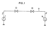
- Fig. 1 illustrates an ordinary DC power feeding system.
- the n-repeaters 1 to n in total are connected in series to the power transmission path C1 and a constant current I is supplied to each repeater from the regulated current feeding equipments 1, 10 provided at both ends of power transmission path.
- the regulated current feeding equipments 1, 10 are provided at both ends because each power feeding equipment is destined to supply the power respectively to n/2-repeaters and thereby a load of one power feeding equipment can be alleviated, and this method is adapted for the system which provides a long transmission distance such as a submarine coaxial transmission system.
- power feeding is carried out by only one power feeding equipment.
- the DC power feeding system illustrated in Fig. 1 is also employed even in the optical fiber cable communication, particularly a submarine optical communication system.
- a power transmission path of conductor is provided within the optical fiber cable and power is fed through this conductor.
- the power transmission path 3 in Fig. 1 is a conductor within the optical fiber cable.
- Fig. 2 illustrates detail of each repeater 1 to n in Fig. 1 and an optical repeater used in the optical communication system which is the object of the present invention.
- an optical repeater has a signal amplifier circuit 42 comprising a photoelectric conversion element, an amplifier circuit and a light emitting element, etc.
- a current I'' branched from the feeding current I' provided through the power transmission path C1 in order to supply the necessary power to the signal amplifier circuit 42 is supplied to said signal amplifier circuit 42 and a voltage V R obtained at both ends of zener diode 41' by applying other branched current I''' to the zener diode 41' is applied to the signal amplifier circuit 42.
- a power V R x I'' is supplied to the signal amplifying circuit 41'.
- C2 is the signal transmission path formed by optical fiber.
- a feeding current I' required for the optical repeater is about 1 to 2A. This value is remarkably larger than the current of 100 to 200 mA which is a feeding current for the coaxial cable. This is because the optical repeater requires a bias current and a drive current for an optical semi-conductor, such as laser diode, A.P.D., therefore larger current is consumed by these in comparison with the coaxial cable system.
- the power feeding equipment tends to be the same as that for dealing with a high voltage.
- a feeding voltage is about 5 kV, but in the optical communication system, it is expected to be about 15 kV for the power feeding equipment.
- selection of circuit elements becomes difficult and mounting of such circuit elements also becomes difficult.
- an optical repeater which is coupled between an optical transmission line composed of optical fibers and a conductor, comprising an electrical circuit for converting input optical signals received from an input side of said optical fibers to electrical signals, for amplifying said electrical signals, for converting the amplified electrical signals to output optical signals, and for transmitting said output optical signals to an output side of said optical fibers, and a power supply circuit connected in series with said conductor for feeding regulated DC current from at least one terminal of said optical transmission line, for receiving said regulated DC current, for dropping the received voltage of said regulated DC current, and for supplying higher DC current than said regulated DC current to said electrical circuit are provided.
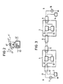
- Fig. 3 is a block diagram indicating an example of structure of the optical communication system to which the present invention is applied.
- an optical terminal A and terminal B are connected with optical fiber cables 3, 5, 6 and 8, and a plurality of optical repeaters 4, 7 are provided between such cables.
- the optical fiber cable is formed by the optical fiber C2 for transmitting optical information and a conductor (power trnsmission path) C1 which is a reinforcing material of the optical fiber and also operates as the power transmission path.
- the optical terminal devices 2, 9 are connected respectively at the terminal A and terminal B.
- Meanwhile, regulated current feeding equipments, regulated current sources 1, 10, are provided at the terminals A, B of the conductor C1.
- the signal amplifier circuits 42, 72 and the current-fed switching type power supply circuits 41, 71 are provided at the optical repeaters 4, 7.
- the signal amplifier circuit 42 is similar to the existing one and comprises a light receiving element 421 which senses the optical signal from the optical fiber C2 i and converts it to an electrical signal, a transistor 422 which amplifies such signal sent from said light receiving element and a light emitting element 423 which receives the amplified signal and emits the light to the next optical fiber C2 o .
- the current-fed switching type voltage drop power supply circuit 41 supplies a necessary power to the signal amplifier circuit 42 and comprises transistors 411, 412, transformer T, rectifying diode D, capacitors Ca, Cb, voltage detection circuit 414 and pulse generating circuit 413.
- the primary side of transformer T is connected to the conductor C1 while the secondary side is used as the power supply of signal amplifier circuit 42 through the rectifying diode D.
- the transistor 411 converts a constant current into an AC voltage through repetition of On and OFF states in accordance with the pulse frequency and pulse width given from the pulse generating circuit 414 and the transformer T drops the AC voltages obtained at both ends a, b of the primary side thereof.
- An AC current obtained at both ends c, d in the secondary side of transformer T is rectified by the diode D is regulated to a constant voltage by controlling the pulse width supplied to the transistor 412 and is supplied as the power to the signal amplifier circuit 42.
- the capacitors Ca and Cb are provided for smoothing.
- the voltage detection circuit 413 trigers the pulse generating circuit 414 when a DC voltage obtained between e and d is higher than the predetermined value causing it to generate the pulse of the predetermined width within the predetermined period. This pulse is applied to the base of transistor 411.
- the voltage detection circuit 413 makes constant a voltage between e and d by controlling the base of transistor 412.
- the current-fed switching type power supply circuit 71 has the structure similar to that of said current-fed switching type voltage drop power supply circuit 41 and provides the similar operations.
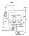
- Fig. 5 illustrates the second embodiment of the present invention.
- the current-fed switching type power supply circuit 41a according to the second embodiment of the present invention is formed with a switched capacitor circuit.
- Recent advancement in ceramic technology has realized a high frequency switching type power supply circuit which does not use electrolytic capacitor and transformer as the switched capacitor circuit with a hybrid IC or LSI utilizing a ceramic capacitor and ceramic substrate.
- the switched capacitor circuit with hybrid IC or LSI is used as the current-fed switching type power supply circuit.
- the switched capacitor circuit 41a comprises the switches SW1-1, SW1-2, SW2-1, SW2-2, ceramic capacitors Cc, Cd, Ce, rectifying diodes D1, D2, D3, D4, voltage detection circuit 501 and pulse generating circuit 502.
- the voltage detection circuit 501 detects an input voltage of the signal amplifying circuit (same as that illustrated in Fig. 4) and triggers the pulse generating circuit 502 in accordance with its input voltage.
- the pulse generating circuit 502 outputs the complementary two pulses P1, P2 having the period and pulse width depending on the output signal of voltage detection circuit 501.
- the pulse P1 controls the switches SW1-1, SW1-2, while the pulse P2 the switches SW1-1, SW2-2. When the switches SW1-1, SW1-2 are ON the switches SW2-1, SW2-2 are OFF. When the switches SW1-1, SW1-2 are OFF, the switches SW2-1, SW2-2 are ON.
- This second embodiment provides excellent effect that long operation life can be assured because a ceramic capacitor is used in place of the electrolytic capacitor and easy mounting is also realized because it is formed as the hybrid IC.
- FIG. 6 An equivalent of the optical communication system comprising the current-fed switching type power supply circuit 41 or 41a considered from the viewpoint of power consumption is illustrated in Fig. 6.
- R c1 , R c2 , ...., R cn are resistances of conductor within the optical fiber cable and R R is equivalent value of power consumption P R within each optical repeater as a resistance.
- This power consumption P R is set to constant for all optical repeaters.
- Fig. 7 indicates such relation.
- the power consumption P R is constant because it does not depend on a feeding current.
- Power loss Pc of coductor is proportional to the square of feeding current.
- a supply voltage V depends on the feeding current and has the property illustrated in Fig. 7.
- a feeding voltage V can be minimized when the power consumption of repeater is equal to that of conductor.
- it is better to reduce a feeding current as much as possible.
- a feeding current is set considering such problem.
- total power is 1.25 kW, which is about 1/3 or less of the existing system.
- the feeding voltage is also 2.5 kV which is equal to that of above case.
- power loss of conductor becomes 0.04 kW which is about 1/4 of the total power of existing system.
- a feeding voltage is 5.2 kV and it does not result in any problem from the viewpoint of high voltage.
- the current-fed switching type power supply circuit being put into practical use assures the conversion efficiency of 80% or more.
- the power loss of such power supply circuit is assumed as 20%, power loss of each repeater becomes 48W and total power becomes 1.45 kW. Therefore, even when considering loss of power supply circuit provided to each repeater, the total power consumption can be suppressed sufficiently in comparison with that of the existing system.
- the optimum feeding current can be set considering factors sch as communication distance and power consumption of repeaters, etc. under the condition that power consumption is minimized and increase of feeding voltage is limited to a certain degree.
- the present invention can remarkably save power consumption of the optical communication system and reduce the size of power feeding equipment by decreasing a feeding current.
Abstract
Description
- The present invention relates to an optical communication system and more specifically to a power feeding system in which at least one optical repeater is provided in the optical communication path, a regulated current feeding equipment which supplies a constant DC current to each repeater is provided at the one end or both ends of the optical communication path and electronic power is supplied to each optical repeater from this regulated current feeding equipment through conductors.
- A power feeding system of the present invention is employed for an ordinary optical communication system and is also suitable for a power feeding system employed for an optical communication system having long transmitting or receiving distance, for example, the submarine optical communication system.
- In various wired transmission system, such as the power feeding system which supplies power from a terminal station to the intermediate repeaters provided along the cable route with a constant interval, a variety of methods where regulated AC or Dc vltage or current is supplied, and repeaters are connected in series or in parallel through the power transmission path are proposed.
- Transmission of AC power requires rectifying and smoothing circuits for the repeaters, resulting in a complicated circuit structure, but it provides such an advantage as freely supplying insulated voltage from a transformer employed. Therefore, this power transmission method is often employed for the transmission system utilizing the electron tube type repeaters which requires many kinds of voltages. However, the power factor is lowered by capacitance and inductance of cables and thereby a voltage drop becomes large and therefore power transmission efficiency (power required for all repeaters/power transmitted) is also lowered. Since DC power feeding is hardly influenced by the cable, it is comparatively easy to supply a constant power to the repeaters and the power transmission efficiency is also high. Accordingly, this method is often employed to the transmission system utilizing transistorized repeaters which is operated by a kind of DC voltage. In addition, since a submarine coaxial transmission system requires high reliability for the repeaters and provides a long power feeding span, a DC power feeding system utilizing less number of parts for the repeater and assures very stable power feeding.
- Fig. 1 illustrates an ordinary DC power feeding system. The n-
repeaters 1 to n in total are connected in series to the power transmission path C1 and a constant current I is supplied to each repeater from the regulatedcurrent feeding equipments current feeding equipments - In the optical transmission system it is impossible to supply the power feeding current superposed on the transmission signal using the communication path itself as in the coaxial cable, a power transmission path of conductor is provided within the optical fiber cable and power is fed through this conductor.
- In this case, the power transmission path 3 in Fig. 1 is a conductor within the optical fiber cable.
- Fig. 2 illustrates detail of each
repeater 1 to n in Fig. 1 and an optical repeater used in the optical communication system which is the object of the present invention. - As illustrated in Fig. 2, an optical repeater has a
signal amplifier circuit 42 comprising a photoelectric conversion element, an amplifier circuit and a light emitting element, etc. A current I'' branched from the feeding current I' provided through the power transmission path C1 in order to supply the necessary power to thesignal amplifier circuit 42 is supplied to saidsignal amplifier circuit 42 and a voltage VR obtained at both ends of zener diode 41' by applying other branched current I''' to the zener diode 41' is applied to thesignal amplifier circuit 42. Thereby, a power VR x I'' is supplied to the signal amplifying circuit 41'. C2 is the signal transmission path formed by optical fiber. The conventional power supply circuit 41' illustrated in Fig. 2 is formed only by a zener diode and it is desirable from the viewpoint of reliability and space, considering the installation condition of optical reepeaters but a feeding current I' required for the optical repeater is about 1 to 2A. This value is remarkably larger than the current of 100 to 200 mA which is a feeding current for the coaxial cable. This is because the optical repeater requires a bias current and a drive current for an optical semi-conductor, such as laser diode, A.P.D., therefore larger current is consumed by these in comparison with the coaxial cable system. - Since power loss in the power transmission path C1 is proportional to the square of feeding current in the case of regulated current feeding system, the power feeding equipment in the conventional optical communication system is considerably enlarged in scale in order to compensate for power loss in the power transmission path C1 and such trend is obvious in the long range transmission system such as the submarine opti cal communication system.
- Particularly, increase of power loss in the power transmission path C1 is a serious problem from the economical viewpoint.
- From this background, the power feeding equipment tends to be the same as that for dealing with a high voltage. For example, in the conventional coaxial cable system, a feeding voltage is about 5 kV, but in the optical communication system, it is expected to be about 15 kV for the power feeding equipment. As the result of employing such high voltage, selection of circuit elements becomes difficult and mounting of such circuit elements also becomes difficult.
- Therefore, it is an object of the present invention to provide an optical repeater which has reduced a feeding current considering that a greater part of feeding power is lost in the power transmission path and power loss increases in proportion to the square of current.
- It is another object of the present invention to provide a regulated current feeding system for optical communication utilizing such an optical repeater.
- According to the present invention, an optical repeater which is coupled between an optical transmission line composed of optical fibers and a conductor, comprising an electrical circuit for converting input optical signals received from an input side of said optical fibers to electrical signals, for amplifying said electrical signals, for converting the amplified electrical signals to output optical signals, and for transmitting said output optical signals to an output side of said optical fibers, and a power supply circuit connected in series with said conductor for feeding regulated DC current from at least one terminal of said optical transmission line, for receiving said regulated DC current, for dropping the received voltage of said regulated DC current, and for supplying higher DC current than said regulated DC current to said electrical circuit are provided.
-
- Fig. 1 illustrates a schematic view of an ordinary regulated current feeding system in the wired transmission system;
- Fig. 2 is a block diagram illustrating each optical repeater in the existing regulated current feeding system for optical communication;
- Fig. 3 is a block diagram illustrating an optical communication system to which the regulated current feeding system for optical communication of the present invention is applied;
- Fig. 4 illustrates schematic diagram of an optical repeater of an embodiment of the present invention;
- Fig. 5 illustrates schematic diagram of an optical repeater of an another embodiment of the present invention;
- Fig. 6 illustrates schematic diagram of an equivalent circuit of Fig. 3;
- Fig. 7 illustrates a characteristic curves indicating power consumption of an optical repeater and power transmission path in the regulated current feeding system.
- The like parts are given the like numeral references throughout the drawings listed above.
- Fig. 3 is a block diagram indicating an example of structure of the optical communication system to which the present invention is applied. In this figure, an optical terminal A and terminal B are connected with
optical fiber cables 3, 5, 6 and 8, and a plurality of optical repeaters 4, 7 are provided between such cables. The optical fiber cable is formed by the optical fiber C2 for transmitting optical information and a conductor (power trnsmission path) C1 which is a reinforcing material of the optical fiber and also operates as the power transmission path. In the optical fiber C2, theoptical terminal devices 2, 9 are connected respectively at the terminal A and terminal B. Meanwhile, regulated current feeding equipments, regulatedcurrent sources - The
signal amplifier circuits power supply circuits - An embodiment of the optical repeater 4 is described with reference to Fig. 4. The
signal amplifier circuit 42 is similar to the existing one and comprises alight receiving element 421 which senses the optical signal from the optical fiber C2i and converts it to an electrical signal, atransistor 422 which amplifies such signal sent from said light receiving element and alight emitting element 423 which receives the amplified signal and emits the light to the next optical fiber C2o. The current-fed switching type voltage droppower supply circuit 41 supplies a necessary power to thesignal amplifier circuit 42 and comprisestransistors pulse generating circuit 413. The primary side of transformer T is connected to the conductor C1 while the secondary side is used as the power supply ofsignal amplifier circuit 42 through the rectifying diode D. - The
transistor 411 converts a constant current into an AC voltage through repetition of On and OFF states in accordance with the pulse frequency and pulse width given from the pulse generating circuit 414 and the transformer T drops the AC voltages obtained at both ends a, b of the primary side thereof. An AC current obtained at both ends c, d in the secondary side of transformer T is rectified by the diode D is regulated to a constant voltage by controlling the pulse width supplied to thetransistor 412 and is supplied as the power to thesignal amplifier circuit 42. The capacitors Ca and Cb are provided for smoothing. Thevoltage detection circuit 413 trigers the pulse generating circuit 414 when a DC voltage obtained between e and d is higher than the predetermined value causing it to generate the pulse of the predetermined width within the predetermined period. This pulse is applied to the base oftransistor 411. Thevoltage detection circuit 413 makes constant a voltage between e and d by controlling the base oftransistor 412. - Since the voltage between c and d of the secondary side is obtained by dropping a voltage between a and b of the primary side with the transformer T, a current I₁ flwoing through the secondary side is higher than the current I supplied to the primary side of transformer T from the regulated
current source 1. It is obvious from the fact that the power supplied to the primary side of transformer T is equal to the power obtained at the secondary side when a loss of transformer T can be neglected. Therefore, it is enough that a current lower than the current required for driving thesignal amplifier circuit 42 is supplied from the regulatedcurrent sources - Since a voltage to be supplied to the
signal amplifier circuit 42 is obtained through the current-fed switching typepower supply circuit 41 utilizing a supply current I as described above, voltage drop of conductor C1 by a regulated current I can be lowered comparatively. Therefore, the problem of the difficulty of selection and mounting of circuit parts due to a high voltage in the prior art can be solved. - Even in the other repeater 7, the current-fed switching type
power supply circuit 71 has the structure similar to that of said current-fed switching type voltage droppower supply circuit 41 and provides the similar operations. - Fig. 5 illustrates the second embodiment of the present invention. In this figure, the current-fed switching type power supply circuit 41a according to the second embodiment of the present invention is formed with a switched capacitor circuit.
- Recent advancement in ceramic technology has realized a high frequency switching type power supply circuit which does not use electrolytic capacitor and transformer as the switched capacitor circuit with a hybrid IC or LSI utilizing a ceramic capacitor and ceramic substrate. In the second embodiment of the present invention, the switched capacitor circuit with hybrid IC or LSI is used as the current-fed switching type power supply circuit.
- In Fig. 5, the switched capacitor circuit 41a comprises the switches SW1-1, SW1-2, SW2-1, SW2-2, ceramic capacitors Cc, Cd, Ce, rectifying diodes D1, D2, D3, D4,
voltage detection circuit 501 andpulse generating circuit 502. - The
voltage detection circuit 501 detects an input voltage of the signal amplifying circuit (same as that illustrated in Fig. 4) and triggers thepulse generating circuit 502 in accordance with its input voltage. Thepulse generating circuit 502 outputs the complementary two pulses P1, P2 having the period and pulse width depending on the output signal ofvoltage detection circuit 501. The pulse P1 controls the switches SW1-1, SW1-2, while the pulse P2 the switches SW1-1, SW2-2. When the switches SW1-1, SW1-2 are ON the switches SW2-1, SW2-2 are OFF. When the switches SW1-1, SW1-2 are OFF, the switches SW2-1, SW2-2 are ON. While the switches SW1-1, SW1-2 are ON, a current flows through the path, capacitor Ce - diode D1 - capacitor Cc, charging the capacitor Cc. But the capacitor Cd is not charged because the switches SW1-2, SW2-2 are OFF. When the switches SW2-1, SW2-2 become ON, a current flows through the path, Ce - D₃ - SW2-2 charging the capacitor Cd. Meanwhile, the capacitor Cc discharges through the path, D₂ - 42 - SW2-1. The capacitors Cd, Ce are connected in parallel for the input ofsignal amplifier circuit 42. Therefore, when the capacitane of capacity and period and pulse width of two pulses output from thepulse generating circuit 502 are adequately set, a voltage which is lower than the charging voltage across the capacitors Cc and Cd or Cd and Ce can be applied to thesignal amplifier circuit 42. As described above, according to the second embodiment of the present invention, it is enough that a current which is lower than that required for driving thesignal amplifier circuit 42 is supplied from the regulatedcurrent source 1. - This second embodiment provides excellent effect that long operation life can be assured because a ceramic capacitor is used in place of the electrolytic capacitor and easy mounting is also realized because it is formed as the hybrid IC.
- An equivalent of the optical communication system comprising the current-fed switching type
power supply circuit 41 or 41a considered from the viewpoint of power consumption is illustrated in Fig. 6. In the same figure, Rc1, Rc2, ...., Rcn are resistances of conductor within the optical fiber cable and RR is equivalent value of power consumption PR within each optical repeater as a resistance. Namely, the power consumption of each optical repeater is equal to sum PR of the power consumption of the current-fed switching type power supply circuit itself and the power consumption of the signal amplifier circuit but it is indicated as PR = I² RR for the feeding current I. This power consumption PR is set to constant for all optical repeaters. Therefore, total power consumption P of this system can be expressed as P = Pc + PR when power loss of conductor is indicated as Pc = I² (Rci) and power loss of optical repeater is indicated as PR = nRR I². Fig. 7 indicates such relation. The power consumption PR is constant because it does not depend on a feeding current. Power loss Pc of coductor is proportional to the square of feeding current. Meanwhile, a supply voltage V depends on the feeding current and has the property illustrated in Fig. 7. - A feeding voltage V can be minimized when the power consumption of repeater is equal to that of conductor. On the other hand, from the point of view of minimizing total power conmsumption, it is better to reduce a feeding current as much as possible. However, if it is extremely reduced, a problem in operation of the current-fed switching type power supply circuit and a problem in increase of feeding voltage are gene rated. Therefore, a feeding current is set considering such problem.
- Above relation is explained hereunder with a practical example. For example, it is assumed that the power consumption of an optical repeater is 40W, a resistance value of conductor is 1 ohm/km and the transmission path of 1000 km is connected through 25 repeaters. In the existing optical communication system, when a feeding current is set to 2A, total power consumption of all repeaters is 1 kW and power loss of conductor is 4 kW. Therefore, total of 5 kW is required as the supply power. In this case, a feeding voltage is 2.5 kV. Meanwhile, when a feeding current is set to 0.5A based on the present invention, power loss of conductor is lowered to 0.25 kW and power consumption of all repeaters is equal to 1 kW. Therefore, total power is 1.25 kW, which is about 1/3 or less of the existing system. In this case, the feeding voltage is also 2.5 kV which is equal to that of above case. Moreover, when a feeding current is set to 0.2A in the present invention, power loss of conductor becomes 0.04 kW which is about 1/4 of the total power of existing system. In this case, a feeding voltage is 5.2 kV and it does not result in any problem from the viewpoint of high voltage.
- Currently, the current-fed switching type power supply circuit being put into practical use assures the conversion efficiency of 80% or more. When the power loss of such power supply circuit is assumed as 20%, power loss of each repeater becomes 48W and total power becomes 1.45 kW. Therefore, even when considering loss of power supply circuit provided to each repeater, the total power consumption can be suppressed sufficiently in comparison with that of the existing system.
- As described above, the optimum feeding current can be set considering factors sch as communication distance and power consumption of repeaters, etc. under the condition that power consumption is minimized and increase of feeding voltage is limited to a certain degree.
- The present invention can remarkably save power consumption of the optical communication system and reduce the size of power feeding equipment by decreasing a feeding current.
- This effect becomes distinctive with increase of communication distance.
Claims (6)
an electrical circuit (42. 72) for converting input optical signals received from an input side of said optical fibers (C2) to electrical signals, for amplifying said electrical signals, for converting the amplified electrical signals to output optical signals, and for transmitting said output optical signals to an output side of said optical fibers, and
a power supply means (41, 71) connected in series with said conductor (C1) for feeding regulated DC current from at least one terminal (A, B) of said optical transmission line, for receiving said regulated DC current, for dropping the received voltage of said regulated DC current, and for supplying higher DC current than said regulated DC current to said electrical circuit (42, 72).
a transformer (T) with the primary side (a, b) connected to said conductor and the secondary side (c, d) connected to said electrical circuit (42, 72),
said secondary side of said transformer (T) outputting a lower voltage than the voltage of said primary side.
an input side connected to said conductor (C1), and output side connected to said electrical circuit (42, 72),
said output side outputting a lower voltage than the voltage of said input side.
means (1, 10) provided at a terminal (A, B) of said optical transmission line for feeding regulated DC current to the repeaters (4, 7) via said conductor (C1),
electrical circuits (42, 72) provided at said repeaters (4, 7) respectively, for converting input optical signals received from an input side of said optical fibers (C2) to electrical signals, for amplifying said electrical signals, for converting the amplified signals to output optical signals, and for transmitting said output optical signals to an output side of said optical fibers (C2), and
power supply means (41, 71) provided at said repeaters (4, 7) respectively, for receiving said regulated DC current from said conductor (C1), for dropping the received voltage of said regulated DC current, and for supplying higher DC than said regulated DC current to said electrical circuit (42, 72)
whereby it is possible to decrease a regulated DC current fed from said means (41, 71).
Applications Claiming Priority (2)
| Application Number | Priority Date | Filing Date | Title |
|---|---|---|---|
| JP262461/85 | 1985-11-25 | ||
| JP60262461A JPS62123842A (en) | 1985-11-25 | 1985-11-25 | Optical communication equipment |
Publications (3)
| Publication Number | Publication Date |
|---|---|
| EP0226801A2 true EP0226801A2 (en) | 1987-07-01 |
| EP0226801A3 EP0226801A3 (en) | 1989-02-01 |
| EP0226801B1 EP0226801B1 (en) | 1994-07-13 |
Family
ID=17376104
Family Applications (1)
| Application Number | Title | Priority Date | Filing Date |
|---|---|---|---|
| EP86115752A Expired - Lifetime EP0226801B1 (en) | 1985-11-25 | 1986-11-13 | Optical repeater and regulated current feeding system for the same |
Country Status (5)
| Country | Link |
|---|---|
| US (1) | US4879762A (en) |
| EP (1) | EP0226801B1 (en) |
| JP (1) | JPS62123842A (en) |
| CA (1) | CA1249342A (en) |
| DE (1) | DE3689970T2 (en) |
Cited By (3)
| Publication number | Priority date | Publication date | Assignee | Title |
|---|---|---|---|---|
| DE3808892A1 (en) * | 1988-03-17 | 1989-09-28 | Standard Elektrik Lorenz Ag | Amplifier for light with equal amplitudes of the output pulses |
| WO2004105268A2 (en) * | 2003-05-14 | 2004-12-02 | Northrop Grumman Corporation | Method and apparatus for branching a single wire power distribution system |
| EP2270967A1 (en) | 2009-06-30 | 2011-01-05 | Alcatel Lucent | System and method for providing electric power to a submerged load |
Families Citing this family (13)
| Publication number | Priority date | Publication date | Assignee | Title |
|---|---|---|---|---|
| JPH04217123A (en) * | 1990-12-18 | 1992-08-07 | Fujitsu Ltd | Feeding system for optical transmission system |
| JPH05122159A (en) * | 1991-05-13 | 1993-05-18 | Internatl Business Mach Corp <Ibm> | Method of improving ratio of signal to noise of transmission signal and optical interconnection system |
| US5777769A (en) * | 1995-12-28 | 1998-07-07 | Lucent Technologies Inc. | Device and method for providing high speed data transfer through a drop line of a power line carrier communication system |
| GB9604427D0 (en) * | 1996-03-01 | 1996-05-01 | Stc Submarine Systems Ltd | A branching unit |
| DE19637417B4 (en) * | 1996-09-13 | 2008-08-14 | Bayerische Motoren Werke Aktiengesellschaft | Operating procedure for a data bus |
| US5945668A (en) * | 1997-06-20 | 1999-08-31 | Sun Microsystems, Inc. | Fiber optic system with open fiber safety interlock |
| DE19833613A1 (en) | 1998-07-25 | 2000-01-27 | Bayerische Motoren Werke Ag | Optical data bus for a vehicle |
| US7233744B1 (en) * | 1999-10-07 | 2007-06-19 | Tyco Telecommunications (Us) Inc. | Power feed arrangement using aggregate segments |
| US20030059156A1 (en) * | 2001-09-24 | 2003-03-27 | Feinberg Lee Daniel | Bifurcated optical and power connectivity for ultra long-haul optical communication systems |
| US20030108351A1 (en) * | 2001-09-24 | 2003-06-12 | Feinberg Lee Daniel | Methods for ultra long-haul optical communications |
| GB2533160A (en) * | 2014-12-12 | 2016-06-15 | Ge Oil & Gas Uk Ltd | Repeaters |
| CN110383717B (en) * | 2017-03-17 | 2022-10-25 | 日本电气株式会社 | Optical submarine cable system and optical submarine repeater |
| FR3078217B1 (en) * | 2018-02-21 | 2020-03-13 | Alstom Transport Technologies | METHOD FOR EXCHANGING DATA IN ELECTRONIC EQUIPMENT, ELECTRONIC EQUIPMENT, RAIL VEHICLE AND RAIL SYSTEM |
Citations (3)
| Publication number | Priority date | Publication date | Assignee | Title |
|---|---|---|---|---|
| JPS56154839A (en) * | 1980-05-01 | 1981-11-30 | Fujitsu Ltd | Power feeding circuit of optical submarine repeater |
| WO1984000849A1 (en) * | 1982-08-23 | 1984-03-01 | Ncr Co | Process for forming an integrated circuit capacitor |
| DE3330045A1 (en) * | 1983-08-19 | 1985-03-07 | Siemens AG, 1000 Berlin und 8000 München | Circuit arrangement for supplying electrical DC load arrangements |
Family Cites Families (4)
| Publication number | Priority date | Publication date | Assignee | Title |
|---|---|---|---|---|
| JPS5172220A (en) * | 1974-12-20 | 1976-06-22 | Hitachi Ltd | |
| US4255782A (en) * | 1977-11-15 | 1981-03-10 | Jgf, Incorporated | Electrical energy conversion systems |
| JPS58187015A (en) * | 1982-04-26 | 1983-11-01 | Nippon Telegr & Teleph Corp <Ntt> | Switched capacitor circuit |
| US4654769A (en) * | 1984-11-02 | 1987-03-31 | California Institute Of Technology | Transformerless dc-to-dc converters with large conversion ratios |
-
1985
- 1985-11-25 JP JP60262461A patent/JPS62123842A/en active Granted
-
1986
- 1986-11-13 DE DE3689970T patent/DE3689970T2/en not_active Expired - Fee Related
- 1986-11-13 EP EP86115752A patent/EP0226801B1/en not_active Expired - Lifetime
- 1986-11-21 US US06/933,114 patent/US4879762A/en not_active Expired - Fee Related
- 1986-11-24 CA CA000523628A patent/CA1249342A/en not_active Expired
Patent Citations (3)
| Publication number | Priority date | Publication date | Assignee | Title |
|---|---|---|---|---|
| JPS56154839A (en) * | 1980-05-01 | 1981-11-30 | Fujitsu Ltd | Power feeding circuit of optical submarine repeater |
| WO1984000849A1 (en) * | 1982-08-23 | 1984-03-01 | Ncr Co | Process for forming an integrated circuit capacitor |
| DE3330045A1 (en) * | 1983-08-19 | 1985-03-07 | Siemens AG, 1000 Berlin und 8000 München | Circuit arrangement for supplying electrical DC load arrangements |
Non-Patent Citations (1)
| Title |
|---|
| PATENT ABSTRACTS OF JAPAN, vol. 10, no. 113 (E-399)[2170], 26th April 1986; & JP-A-60 249 444 (FUJITSU K.K.) 10-12-1985 * |
Cited By (5)
| Publication number | Priority date | Publication date | Assignee | Title |
|---|---|---|---|---|
| DE3808892A1 (en) * | 1988-03-17 | 1989-09-28 | Standard Elektrik Lorenz Ag | Amplifier for light with equal amplitudes of the output pulses |
| WO2004105268A2 (en) * | 2003-05-14 | 2004-12-02 | Northrop Grumman Corporation | Method and apparatus for branching a single wire power distribution system |
| WO2004105268A3 (en) * | 2003-05-14 | 2005-01-06 | Northrop Grumman Corp | Method and apparatus for branching a single wire power distribution system |
| EP2270967A1 (en) | 2009-06-30 | 2011-01-05 | Alcatel Lucent | System and method for providing electric power to a submerged load |
| WO2011000742A1 (en) * | 2009-06-30 | 2011-01-06 | Alcatel Lucent | System and method for providing electric power to a submerged load |
Also Published As
| Publication number | Publication date |
|---|---|
| JPS62123842A (en) | 1987-06-05 |
| CA1249342A (en) | 1989-01-24 |
| EP0226801A3 (en) | 1989-02-01 |
| JPH0420538B2 (en) | 1992-04-03 |
| EP0226801B1 (en) | 1994-07-13 |
| US4879762A (en) | 1989-11-07 |
| DE3689970D1 (en) | 1994-08-18 |
| DE3689970T2 (en) | 1994-12-08 |
Similar Documents
| Publication | Publication Date | Title |
|---|---|---|
| EP0226801A2 (en) | Optical repeater and regulated current feeding system for the same | |
| US5838116A (en) | Fluorescent light ballast with information transmission circuitry | |
| CA2197975A1 (en) | Universal power module | |
| JP2005512486A (en) | Power converter | |
| CN101621877A (en) | Current feed circuit and current control circuit of light emitting diode | |
| US20040061506A1 (en) | Method for evaluating a measuring signal and corresponding circuit arrangement | |
| Heinig et al. | Single-fiber combined optical power and data transmission for high-voltage applications | |
| JP2001025180A (en) | Optical power feeding device | |
| JPH1189120A (en) | Optical power transmitting method and device | |
| EP3435551B1 (en) | Current pulse transformer for isolating electrical signals | |
| CN112332670B (en) | Multi-group multi-voltage output flyback converter control circuit | |
| CN216564925U (en) | Multi-output power supply | |
| JPH1189113A (en) | Uninterruptive power supply unit | |
| CN115021574A (en) | Power supply chip | |
| JPH06276702A (en) | Photoelectric power supply method | |
| US7116013B2 (en) | Electronic power source voltage regulator with UPS function | |
| US4924369A (en) | Regulated blocking converter wherein switch conduction time increases with higher output voltages | |
| WO2019186685A1 (en) | Contactless power receiving device and contactless power supply system | |
| KR950001264B1 (en) | Data communication system | |
| CN100407537C (en) | Switch type power supply protective circuit in electronic equipment | |
| CN210721185U (en) | Second-order voltage stabilizing circuit based on load size | |
| CN220933410U (en) | Constant voltage and constant current compensation circuit and electronic equipment | |
| CN219833801U (en) | Charger circuit and chip | |
| CN212258794U (en) | Open-loop half-bridge resonant circuit for multi-path voltage output | |
| Garinto | On Digital Power Transmission Systems |
Legal Events
| Date | Code | Title | Description |
|---|---|---|---|
| PUAI | Public reference made under article 153(3) epc to a published international application that has entered the european phase |
Free format text: ORIGINAL CODE: 0009012 |
|
| AK | Designated contracting states |
Kind code of ref document: A2 Designated state(s): DE FR GB |
|
| PUAL | Search report despatched |
Free format text: ORIGINAL CODE: 0009013 |
|
| AK | Designated contracting states |
Kind code of ref document: A3 Designated state(s): DE FR GB |
|
| 17P | Request for examination filed |
Effective date: 19890403 |
|
| 17Q | First examination report despatched |
Effective date: 19910411 |
|
| GRAA | (expected) grant |
Free format text: ORIGINAL CODE: 0009210 |
|
| AK | Designated contracting states |
Kind code of ref document: B1 Designated state(s): DE FR GB |
|
| REF | Corresponds to: |
Ref document number: 3689970 Country of ref document: DE Date of ref document: 19940818 |
|
| ET | Fr: translation filed | ||
| PLBE | No opposition filed within time limit |
Free format text: ORIGINAL CODE: 0009261 |
|
| STAA | Information on the status of an ep patent application or granted ep patent |
Free format text: STATUS: NO OPPOSITION FILED WITHIN TIME LIMIT |
|
| 26N | No opposition filed | ||
| PGFP | Annual fee paid to national office [announced via postgrant information from national office to epo] |
Ref country code: FR Payment date: 19991109 Year of fee payment: 14 |
|
| PGFP | Annual fee paid to national office [announced via postgrant information from national office to epo] |
Ref country code: GB Payment date: 19991110 Year of fee payment: 14 |
|
| PGFP | Annual fee paid to national office [announced via postgrant information from national office to epo] |
Ref country code: DE Payment date: 19991115 Year of fee payment: 14 |
|
| PG25 | Lapsed in a contracting state [announced via postgrant information from national office to epo] |
Ref country code: GB Free format text: LAPSE BECAUSE OF NON-PAYMENT OF DUE FEES Effective date: 20001113 |
|
| GBPC | Gb: european patent ceased through non-payment of renewal fee |
Effective date: 20001113 |
|
| PG25 | Lapsed in a contracting state [announced via postgrant information from national office to epo] |
Ref country code: FR Free format text: LAPSE BECAUSE OF NON-PAYMENT OF DUE FEES Effective date: 20010731 |
|
| PG25 | Lapsed in a contracting state [announced via postgrant information from national office to epo] |
Ref country code: DE Free format text: LAPSE BECAUSE OF NON-PAYMENT OF DUE FEES Effective date: 20010801 |
|
| REG | Reference to a national code |
Ref country code: FR Ref legal event code: ST |