EP0225441B1 - Programmierstrom-Steuergerät - Google Patents
Programmierstrom-Steuergerät Download PDFInfo
- Publication number
- EP0225441B1 EP0225441B1 EP86112823A EP86112823A EP0225441B1 EP 0225441 B1 EP0225441 B1 EP 0225441B1 EP 86112823 A EP86112823 A EP 86112823A EP 86112823 A EP86112823 A EP 86112823A EP 0225441 B1 EP0225441 B1 EP 0225441B1
- Authority
- EP
- European Patent Office
- Prior art keywords
- transistor
- transistors
- floating gate
- array
- current
- Prior art date
- Legal status (The legal status is an assumption and is not a legal conclusion. Google has not performed a legal analysis and makes no representation as to the accuracy of the status listed.)
- Expired
Links
- 238000000034 method Methods 0.000 claims description 13
- 230000005669 field effect Effects 0.000 claims description 8
- 239000004065 semiconductor Substances 0.000 claims description 5
- 238000009792 diffusion process Methods 0.000 claims description 3
- 229910021420 polycrystalline silicon Inorganic materials 0.000 claims description 3
- 229920005591 polysilicon Polymers 0.000 claims description 3
- 230000008569 process Effects 0.000 claims description 3
- 239000000463 material Substances 0.000 claims 1
- 229910052710 silicon Inorganic materials 0.000 claims 1
- 239000010703 silicon Substances 0.000 claims 1
- 238000010586 diagram Methods 0.000 description 3
- 238000004519 manufacturing process Methods 0.000 description 3
- 230000006870 function Effects 0.000 description 2
- 230000004048 modification Effects 0.000 description 2
- 238000012986 modification Methods 0.000 description 2
- 230000008859 change Effects 0.000 description 1
Images
Classifications
-
- G—PHYSICS
- G11—INFORMATION STORAGE
- G11C—STATIC STORES
- G11C16/00—Erasable programmable read-only memories
- G11C16/02—Erasable programmable read-only memories electrically programmable
- G11C16/06—Auxiliary circuits, e.g. for writing into memory
- G11C16/10—Programming or data input circuits
Definitions
- the present invention relates to a programming current controlling method and device for an electrically erasable programmable semiconductor memory cell.
- the invention is directed, more particularly, to a programming current controlling device which is formed on a chip containing a plurality of such memory cells in an array.
- the invention yet more particularly, relates to an electrically programmable semiconductor memory device having an array of floating gate transistors sets of which are coupled between associated respective source and drain lines, a array programming control transistor and a ground select transistor coupled to each of said drain and source lines such that each selected floating gate transistor in a programming mode is in series with said control and ground select transistors between a high voltage Vpp, and ground potential.
- Such an arrangement is exemplified in, for example, United States Patent 4,404,659.
- an electrically programmable semiconductor memory device as set forth in Claim 1.
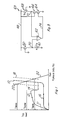
- FIG. 1 there is shown a typical characteristic of the source/drain voltage versus the source/drain current of an EPROM memory cell.
- the forward path in the linear region 11 exhibits a rapid initial current rise with increasing voltage enters the saturation region 12 and then drops off rapidly at 14 where programming begins.
- the drain current stays flat for a few volts and there is a sudden large linear increase in current with increasing voltage 10.
- the return path follows path 10, then the long horizontal portion 16 before dropping to zero current.
- a typical load line 22 is also shown in which a high voltage V pp is applied through a programming load device.
- the nominal operating point or programming current is Inom.
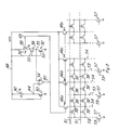
- a programming current controller as shown in Figure 2 includes a resistive element 42 in a reference current leg in series with a reference ground select transistor 30 which is biased on by having its gate connected to the high voltage line Vpp 48. As a consequence of a reference current I R being established through transistor 30, a voltage V1 will be established at junction 44.
- a module programming control P-channel field effect transistor 36 is in series with a module floating gate transistor 38 and an N-channel control select field effect transistor 32 identical to transistor 30, coupled between line 48 and ground. Both the transistor 38 and the transistor 32 are biased on by having their control gate 52 and gate 50, respectively, connected to line 48.
- the current 1 A is controlled by the module programming control transistor 36 and in flowing through the control select transistor 32 develops a voltage V2 at junction 35.
- Junction 44 is coupled to the inverting input of comparator 34 while junction 35 is connected to the non-inverting input thereof.
- the comparator output 40 is coupled to the gate 46 of module programming control transistor 36 as well as being coupled to gates of matching array control transistors 46a, 46b, 46c, etc.
- Each of the programming control transistors 46a, 46b, etc. are coupled to corresponding column lines 54 each one of which connects to a parallel array of floating gate transistors 38 ⁇ .
- the other end of the parallel array of transistors 38 ⁇ are connected to corresponding decoded ground lines 53 each of which is coupled to ground through a ground select transistor 57 the gates of which 59 are used to select the active ground line.
- reference ground select transistor 30 being in a conductive state causes a current I R to flow through resistive element 42 the value of which is determined by Vpp less the voltage across transistor 30 divided by the value of resistance of element 42.
- a voltage V1 at junction 44 is developed which is applied to the inverting input of comparator 34.
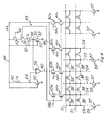
- the array of Figure 2 may be modified as shown in Figure 4 by introducing column select transistors 60a, 60b, 60c ... etc., in respective columns 54 between V pp line 48 and respective transistors 46a, 46b, etc and P-channel transistor 47 in series with P-channel transistor 36.
- An appropriate one or more of column lines 54 are selected by driving the gates 58 of column select transistors 60 low. Otherwise the operation of the circuit of Figure 4 is the same as that of Figure 2.
- Transistor 47 is used to make the second leg identical to each column of the array.
Landscapes
- Read Only Memory (AREA)
- Semiconductor Memories (AREA)
Claims (19)
- Elektrisch programmierbare Halbleiterspeichervorrichtung mit einer Matrix aus Transistoren (38') mit nicht angeschlossenem Gate, von denen Gruppen zwischen zugeordneten jeweiligen Source- und Drain-Leitungen (53, 54) angeschlossen sind, einem Matrixprogrammier-Steuertransistor (46a-x) und einem Massewähltransistor (57), die an jede der Drain- und Source-Leitungen so angeschlossen sind, daß jeder ausgewählte Transistor mit nicht angeschlossenem Gate in einem Programmiermodus in Serie mit den Steuer- und Massewähltransistoren zwischen einer hohen Spannung Vpp und Massepotential liegt, dadurch gekennzeichnet, daß sie folgendes enthält:
ein widerstandsbehaftetes Element (42) in Serie mit einem ersten widerstandsbehafteten Schaltungselement (30), das zwischen Vpp und Masse angeschlossen ist, wobei eine Spannung V₁ am Verbindungspunkt (44) des widerstandsbehafteten Elements und des ersten widerstandsbehafteten Schaltungselements erzeugt wird;
ein zweites widerstandsbehaftetes Schaltungslement (32), einen in einen leitenden Zustand vorgespannten Modul-Transistor (38) mit nicht angeschlossenem Gate sowie einem Modulprogrammier-Steuertransistor (46), wobei alle diese Transistoren in Serie zwischen Vpp und Masse geschaltet sind, wodurch eine Spannung V₂ am Verbindungspunkt (35) des zweiten widerstandsbehafteten Schaltungselements und des Modul-Transistors mit nicht angeschlossenem Gate erzeugt wird; und
ein Mittel (43) zum Vergleichen von V₁ und V₂ und zum Einstellen der Gate-Spannung V₃ des Modul-Steuertransistors in der Weise, daß die Spannung V₂ gleich V₁ gemacht wird und V₃ an die Gate-Elektroden der Matrix-Steuertransistoren angelegt wird. - Speichervorrichtung nach Anspruch 1, bei welcher das erste widerstandsbehaftete Schaltungselement und das zweite widerstandsbehaftete Schaltungselement Referenzwähl- bzw. Massewähl-Transisoren sind, die beide in den leitenden Zustand vorgespannt sind.
- Speichervorrichtung nach Anspruch 2, bei welcher die Vergleichsmittel von einem Komparator gebildet sind, bei dem ein Eingang mit dem Verbindungspunkt des widerstandsbehafteten Elements und des Referenzwähl-Transistors verbunden ist und ein weiterer Eingang mit dem Verbindungspunkt des Massewähltransistors und des Modul-Transistors mit nicht angeschlossenem Gate verbunden ist, und ein Ausgang mit den Gate-Elektroden des Modulprogrammier-Steuertransistors und den Matrixprogrammier-Steuertransistoren verbunden ist.
- Speichervorrichtung nach Anspruch 3, bei welcher das Halbleitermaterial Silicium ist.
- Speichervorrichtung nach Anspruch 3, bei welcher die Modulprogrammier- und die Matrixprogrammier-Steuertransistoren P-Kanal-Feldeffekttransistoren sind.
- Speichervorrichtung nach Anspruch 5, bei welcher die Modulprogrammier- und die Matrixprogrammier-Steuertransistoren N-Kanal-Feldeffekttransistoren sind.
- Speichervorrichtung nach Anspruch 4, dadurch gekennzeichnet, daß die Matrixprogrammier-Steuertransistoren und die Transistoren mit nicht angeschlossenem Gate durch den gleichen Prozeß wie die Modulprogrammier-Steuertransistoren und die Modul-Transistoren mit nicht angeschlossenem Gate hergestellt sind.
- Speichervorrichtung nach Anspruch 3, bei welcher das widerstandsbehaftete Element ein bipolarer Transistor ist.
- Speichervorrichtung nach Anspruch 3, bei welcher das widerstandsbehaftete Element ein Diffusionswiderstand ist.
- Speichervorrichtung nach Anspruch 3, bei welcher das widerstandsbehaftete Element ein Widerstand aus polykristallinem Silicium ist.
- Speichervorrichtung nach Anspruch 3, bei welcher das widerstandsbehaftete Element ein MOS-Transistor ist.
- Verfahren zum Steuern des Programmierstroms einer Matrix aus elektrisch programmierbaren Festspeichertransistoren mit nicht angeschlossenem Gate nach Anspruch 1, enthaltend die Schritte:
Erzeugen eines gewünschten Bezugsstroms;
Vergleichen einer durch den Bezugsstrom an einem Schaltungselement in einem Strompfad erzeugten Spannung V₁ mit einer an einem ähnlichen Schaltungselement in einem anderen Strompfad mit ähnlichen Schaltungselementen wie den Schaltungselementen in einem Pfad eines ausgewählten Transistors der Matrixtransistoren mit nicht angeschlossenem Gate erzeugten Spannung V₂;
Anlegen von V₁ an einen invertierenden Eingang und von V₂ an einen nichtinvertierenden Eingang eines Komparators und Anlegen des Komparatorausgangssignals an eine Gate-Elektrode eines Modulprogrammier-Steuertransistors in dem anderen Strompfad, so daß die Spannung an dem Modulprogrammier-Steuertransistor sich in Abhängigkeit vom Ausgangssignal des Komparators so ändert, daß der Strom in dem anderen Strompfad im wesentlichen gleich dem Bezugsstrom gehalten wird;
und Anlegen des Komparatorausgangssignals an eine Gate-Elektrode eines Matrixprogrammier-Steuertransistors, der in Serie mit dem ausgewählten Matrixtransistor mit nicht angeschlossenem Gate liegt, so daß der durch den ausgewählten Transistor mit nicht angeschlossenem Gate im wesentlichen gleich dem Bezugsstrom gehalten wird. - Verfahren nach Anspruch 12, bei welchem das Schaltungselement in dem Strompfad des Bezugsstroms, das das gleiche wie ein entsprechendes Schaltungselement in dem anderen Pfad ist, ein Feldeffekttransistor ist.
- Verfahren nach Anspruch 13, bei welchem die Schaltungselemente in dem anderen Strompfad zusätzlich zu einem Feldeffekttransistor ein elektrisch programmierbarer Transistor mit nicht angeschlossenem Gate und ein zweiter Feldeffekttransistor sind.
- Verfahren nach Anspruch 14, bei welchem die Schaltungselemente in dem Strompfad des Bezugsstroms ein widerstandsbehaftetes Element enthalten, das in Serie mit dem Feldeffekttransistor geschaltet ist, der in einen leitenden Zustand vorgespannt ist.
- Verfahren nach Anspruch 15, bei welchem das widerstandsbehaftete Element ein bipolarer Transistor ist.
- Verfahren nach Anspruch 15, bei welchem das widerstandsbehaftete Element ein Diffusionswiderstand ist.
- Verfahren nach Anspruch 15, bei welchem das widerstandsbehaftete Element ein Widerstand aus polykristallinem Silicium ist.
- Verfahren nach Anspruch 15, bei welchem das widerstandsbehaftete Element ein MOS-Transistor ist.
Applications Claiming Priority (2)
| Application Number | Priority Date | Filing Date | Title |
|---|---|---|---|
| US06/786,981 US4723225A (en) | 1985-10-15 | 1985-10-15 | Programming current controller |
| US786981 | 1985-10-15 |
Publications (3)
| Publication Number | Publication Date |
|---|---|
| EP0225441A2 EP0225441A2 (de) | 1987-06-16 |
| EP0225441A3 EP0225441A3 (en) | 1989-03-08 |
| EP0225441B1 true EP0225441B1 (de) | 1992-02-19 |
Family
ID=25140103
Family Applications (1)
| Application Number | Title | Priority Date | Filing Date |
|---|---|---|---|
| EP86112823A Expired EP0225441B1 (de) | 1985-10-15 | 1986-09-17 | Programmierstrom-Steuergerät |
Country Status (4)
| Country | Link |
|---|---|
| US (1) | US4723225A (de) |
| EP (1) | EP0225441B1 (de) |
| JP (1) | JPS62177797A (de) |
| DE (1) | DE3683930D1 (de) |
Families Citing this family (20)
| Publication number | Priority date | Publication date | Assignee | Title |
|---|---|---|---|---|
| US5367208A (en) | 1986-09-19 | 1994-11-22 | Actel Corporation | Reconfigurable programmable interconnect architecture |
| JPS6432494A (en) * | 1987-07-27 | 1989-02-02 | Mitsubishi Electric Corp | Non-volatile semiconductor storage device |
| US4868790A (en) * | 1988-04-28 | 1989-09-19 | Texas Instruments Incorporated | Reference circuit for integrated memory arrays having virtual ground connections |
| US5042009A (en) * | 1988-12-09 | 1991-08-20 | Waferscale Integration, Inc. | Method for programming a floating gate memory device |
| KR910007434B1 (ko) * | 1988-12-15 | 1991-09-26 | 삼성전자 주식회사 | 전기적으로 소거 및 프로그램 가능한 반도체 메모리장치 및 그 소거 및 프로그램 방법 |
| US5299150A (en) * | 1989-01-10 | 1994-03-29 | Actel Corporation | Circuit for preventing false programming of anti-fuse elements |
| US5177705A (en) * | 1989-09-05 | 1993-01-05 | Texas Instruments Incorporated | Programming of an electrically-erasable, electrically-programmable, read-only memory array |
| US5027321A (en) * | 1989-11-21 | 1991-06-25 | Intel Corporation | Apparatus and method for improved reading/programming of virtual ground EPROM arrays |
| US5128895A (en) * | 1989-11-21 | 1992-07-07 | Intel Corporation | Method for programming a virtual ground EPROM cell including slow ramping of the column line voltage |
| EP0432481A3 (en) * | 1989-12-14 | 1992-04-29 | Texas Instruments Incorporated | Methods and apparatus for verifying the state of a plurality of electrically programmable memory cells |
| JP2606941B2 (ja) * | 1990-02-19 | 1997-05-07 | 富士通株式会社 | 不揮発性メモリの書込み回路 |
| US5132933A (en) * | 1990-12-21 | 1992-07-21 | Schreck John F | Bias circuitry for nonvolatile memory array |
| US5491658A (en) * | 1991-02-13 | 1996-02-13 | Texas Instruments Incorporated | Column decoder for virtual ground memory array |
| US5719806A (en) * | 1991-02-18 | 1998-02-17 | Yamane; Masatoshi | Memory cell array |
| US5367213A (en) * | 1993-06-09 | 1994-11-22 | Micron Semiconductor, Inc. | P-channel sense amplifier pull-up circuit incorporating a voltage comparator for use in DRAM memories having non-bootstrapped word lines |
| FR2718273B1 (fr) * | 1994-03-31 | 1996-05-24 | Sgs Thomson Microelectronics | Mémoire intégrée avec circuit de maintien de la tension de colonne. |
| US5481492A (en) * | 1994-12-14 | 1996-01-02 | The United States Of America As Represented By The Secretary Of The Navy | Floating gate injection voltage regulator |
| JP4715024B2 (ja) * | 2001-05-08 | 2011-07-06 | セイコーエプソン株式会社 | 不揮発性半導体記憶装置のプログラム方法 |
| JP2002334588A (ja) * | 2001-05-11 | 2002-11-22 | Seiko Epson Corp | 不揮発性半導体記憶装置のプログラム方法 |
| US20110002161A1 (en) * | 2009-07-06 | 2011-01-06 | Seagate Technology Llc | Phase change memory cell with selecting element |
Family Cites Families (4)
| Publication number | Priority date | Publication date | Assignee | Title |
|---|---|---|---|---|
| US4218764A (en) * | 1978-10-03 | 1980-08-19 | Matsushita Electric Industrial Co., Ltd. | Non-volatile memory refresh control circuit |
| JPS5654693A (en) * | 1979-10-05 | 1981-05-14 | Hitachi Ltd | Programable rom |
| US4387447A (en) * | 1980-02-04 | 1983-06-07 | Texas Instruments Incorporated | Column and ground select sequence in electrically programmable memory |
| NL8400661A (nl) * | 1984-03-01 | 1985-10-01 | Philips Nv | Halfgeleiderinrichting met tenminste een niet-vluchtige geheugentransistor. |
-
1985
- 1985-10-15 US US06/786,981 patent/US4723225A/en not_active Expired - Lifetime
-
1986
- 1986-09-17 DE DE8686112823T patent/DE3683930D1/de not_active Expired - Lifetime
- 1986-09-17 EP EP86112823A patent/EP0225441B1/de not_active Expired
- 1986-10-14 JP JP61244006A patent/JPS62177797A/ja active Granted
Also Published As
| Publication number | Publication date |
|---|---|
| DE3683930D1 (de) | 1992-03-26 |
| US4723225A (en) | 1988-02-02 |
| EP0225441A3 (en) | 1989-03-08 |
| JPH0529996B2 (de) | 1993-05-06 |
| JPS62177797A (ja) | 1987-08-04 |
| EP0225441A2 (de) | 1987-06-16 |
Similar Documents
| Publication | Publication Date | Title |
|---|---|---|
| EP0225441B1 (de) | Programmierstrom-Steuergerät | |
| US5218571A (en) | EPROM source bias circuit with compensation for processing characteristics | |
| US5253201A (en) | Writing control circuit employed in non-volatile semiconductor memory device | |
| US5142495A (en) | Variable load for margin mode | |
| US5706240A (en) | Voltage regulator for memory device | |
| US5406141A (en) | High voltage CMOS switching circuit | |
| US4874967A (en) | Low power voltage clamp circuit | |
| JPH04132088A (ja) | 半導体メモリ素子の高電圧発生回路 | |
| EP0729633B1 (de) | Leseverstärker für nicht-flüchtigen halbleiterspeicher | |
| US5905677A (en) | Voltage regulator for non-volatile semiconductor electrically programmable memory devices | |
| JP2851035B2 (ja) | プログラム可能な論理装置 | |
| US4843594A (en) | Nonvolatile semiconductor memory device with a bias circuit | |
| KR100322471B1 (ko) | 불휘발성 반도체 메모리 장치의 감지 증폭기 회로 | |
| US5117392A (en) | Non-volatile semiconductor memory device | |
| US5872733A (en) | Ramp-up rate control circuit for flash memory charge pump | |
| JPH05102402A (ja) | 半導体装置 | |
| KR100382037B1 (ko) | 정전압회로를 갖는 반도체 기억장치 | |
| EP0225442B1 (de) | Entzerrte Matrixvorspannung für PROMS und EPROMS | |
| EP0183476B1 (de) | MOS-Festwertspeicher | |
| US5691944A (en) | Non-volatile semiconductor memory device | |
| KR19990071743A (ko) | 고전압레벨시프팅cmos버퍼 | |
| EP0346671B1 (de) | Programmierung eines EPROMs | |
| EP0757358B1 (de) | Leseschaltung für nichtflüchtige Speicher | |
| US5617370A (en) | Semiconductor memory device with controllable charging characteristics of column lines | |
| JPH0737385A (ja) | 内部電源用降圧回路 |
Legal Events
| Date | Code | Title | Description |
|---|---|---|---|
| PUAI | Public reference made under article 153(3) epc to a published international application that has entered the european phase |
Free format text: ORIGINAL CODE: 0009012 |
|
| AK | Designated contracting states |
Kind code of ref document: A2 Designated state(s): DE FR GB |
|
| PUAL | Search report despatched |
Free format text: ORIGINAL CODE: 0009013 |
|
| AK | Designated contracting states |
Kind code of ref document: A3 Designated state(s): DE FR GB |
|
| 17P | Request for examination filed |
Effective date: 19890721 |
|
| 17Q | First examination report despatched |
Effective date: 19901128 |
|
| GRAA | (expected) grant |
Free format text: ORIGINAL CODE: 0009210 |
|
| AK | Designated contracting states |
Kind code of ref document: B1 Designated state(s): DE FR GB |
|
| REF | Corresponds to: |
Ref document number: 3683930 Country of ref document: DE Date of ref document: 19920326 |
|
| ET | Fr: translation filed | ||
| PLBE | No opposition filed within time limit |
Free format text: ORIGINAL CODE: 0009261 |
|
| STAA | Information on the status of an ep patent application or granted ep patent |
Free format text: STATUS: NO OPPOSITION FILED WITHIN TIME LIMIT |
|
| 26N | No opposition filed | ||
| REG | Reference to a national code |
Ref country code: GB Ref legal event code: IF02 |
|
| PGFP | Annual fee paid to national office [announced via postgrant information from national office to epo] |
Ref country code: DE Payment date: 20030930 Year of fee payment: 18 |
|
| PG25 | Lapsed in a contracting state [announced via postgrant information from national office to epo] |
Ref country code: DE Free format text: LAPSE BECAUSE OF NON-PAYMENT OF DUE FEES Effective date: 20050401 |
|
| PGFP | Annual fee paid to national office [announced via postgrant information from national office to epo] |
Ref country code: GB Payment date: 20050809 Year of fee payment: 20 |
|
| PGFP | Annual fee paid to national office [announced via postgrant information from national office to epo] |
Ref country code: FR Payment date: 20050902 Year of fee payment: 20 |
|
| PG25 | Lapsed in a contracting state [announced via postgrant information from national office to epo] |
Ref country code: GB Free format text: LAPSE BECAUSE OF EXPIRATION OF PROTECTION Effective date: 20060916 |
|
| REG | Reference to a national code |
Ref country code: GB Ref legal event code: PE20 |