EP0225441A2 - Programmierstrom-Steuergerät - Google Patents
Programmierstrom-Steuergerät Download PDFInfo
- Publication number
- EP0225441A2 EP0225441A2 EP86112823A EP86112823A EP0225441A2 EP 0225441 A2 EP0225441 A2 EP 0225441A2 EP 86112823 A EP86112823 A EP 86112823A EP 86112823 A EP86112823 A EP 86112823A EP 0225441 A2 EP0225441 A2 EP 0225441A2
- Authority
- EP
- European Patent Office
- Prior art keywords
- transistor
- transistors
- voltage
- floating gate
- array
- Prior art date
- Legal status (The legal status is an assumption and is not a legal conclusion. Google has not performed a legal analysis and makes no representation as to the accuracy of the status listed.)
- Granted
Links
Images


Classifications
-
- G—PHYSICS
- G11—INFORMATION STORAGE
- G11C—STATIC STORES
- G11C16/00—Erasable programmable read-only memories
- G11C16/02—Erasable programmable read-only memories electrically programmable
- G11C16/06—Auxiliary circuits, e.g. for writing into memory
- G11C16/10—Programming or data input circuits
Definitions
- the present invention relates to a programming current controlling method and device for an electrically erasable programmable semiconductor memory cell.
- the invention is directed, more particularly, to a programming current controlling device which is formed on a chip containing a plurality of such memory cells in an array.
- the programming current for an EPROM depends both on circuit elements coupled to the EPROM cell as well as on the characteristics of the EPROM cell itself. Since the programming load line normally chosen passes through a steeply sloped portion of the curve and is itself steeply sloped any relatively small variation in the curve results in a relatively significant variation in programming current. The programming current must be maintained between an I MIN value determined by the minimum current required to program the EPROM cell and IMAX set by the I pp specification. In the case of low programming current long programming times result whereas high programming currents may fail the specification for maximum allowable programming current.
- an electrically programmable semiconductor memory device of a type having an array of programmable semiconductor floating gate transistors sets of which are coupled between associated respective source and drain lines, an array programming control transistor and a ground select transistor coupled to each of the drain and source lines.
- Each selected floating gate transistor in a programming mode is in series with control and ground select transistors between a high voltage Vpp and ground potential.
- a resistive element in series with a first conducting circuit element establishes a reference current which generates a voltage V1 at the junction of the resistive element and the circuit element.
- a module floating gate transistor biased into a conducting state and a module control transistor are all connected between Vpp and ground such that a voltage V2 is established at the junction of the second circuit element and the module floating gate transistor.
- Comparing means compares voltages V1 and V2 and adjusts the gate voltage V3 of the module programming control transistor so as to make the voltage V2 equal to voltage V1 and applies voltage V3 to the gates of the array programming control transistors. Since the transistor in the reference path is both electrically and geometrically the same as that in the second leg across which the voltage developed is compared, and is made by the same process, the current in the second leg will be substantially the same as that in the reference leg.
- array floating gate transistors are also made by the same process as is the module floating gate transistor and the programming control and ground select transistors are also identical, by feeding the voltage V3 to array control transistors substantially the same current will flow through a selected array transistor as flows through both the reference current path and the second current leg.
- FIG. 1 there is shown a typical characteristic of the source/drain voltage versus the source/drain current of an EPROM memory cell.
- the forward path in the linear region 11 exhibits a rapid initial current rise with increasing voltage enters the saturation region 12 and then drops off rapidly at 14 where programming begins.
- the drain current stays flat for a few volts and there is a sudden large linear increase in current with increasing voltage 10.
- the return path follows path 10, then the long horizontal portion 16 before dropping to zero current.
- a typical load line 22 is also shown in which a high voltage V pp is applied through a programming load device.
- the nominal operating point or programming current is Inom.
- Path 10 is a function of the channel length of the memory cell and is subject to up to a 2 volt variation. This will cause a range of cell programming currents from I MIN to I MAX . This change in programming current will directly affect programming time. Such a large variation in programming time creates severe production problems in terms of low yield and associated marketability. For the low current end the programming time is excessively long while for the higher current the maximum allowable programming current will be exceeded.
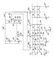
- a programming current controller as shown in Figure 2 includes a resistive element 42 in a reference current leg in series with a reference ground select transistor 30 which is biased on by having its gate connected to the high voltage line Vpp 48. As a consequence of a reference current I R being established through transistor 30, a voltage V1 will be established at junction 44.
- a module programming control P-channel field effect transistor 36 is in series with a module floating gate transistor 52 and an N-channel control select field effect transistor 32 identical to transistor 30, coupled between line 48 and ground. Both the transistor 38 and the transistor 30 are biased on by having their control gate 52 and gate 50, respectively, connected to line 48.
- the current 1 A is controlled by the module programming control transistor 36 and in flowing through the control select transistor 32 develops a voltage V2 at junction 35.
- Junction 44 is coupled to the inverting input of comparator 34 while junction 35 is connected to the non-inverting input thereof.
- the comparator output 40 is coupled to the gate 46 of module programming control transistor 36 as well as being coupled to gates of matching array control transistors 46a, 46b, 46c, etc.
- Each of the programming control transistors 46a, 46b, etc. are coupled to corresponding column lines 54 each one of which connects to a parallel array of floating gate transistors 38 ⁇ .
- the other end of the parallel array of transistors 38 ⁇ are connected to corresponding decoded ground lines 53 each of which is coupled to ground through a ground select transistor 57 the gates of which 59 are used to select the active ground line.
- reference ground select transistor 30 being in a conductive state causes a current I R to flow through resistive element 42 the value of which is determined by Vpp less the voltage across transistor 30 divided by the value of resistance of element 42.
- a voltage V1 at junction 44 is developed which is applied to the inverting input of comparator 34.
- the comparator output 40 swings the voltage on the gate 46 of transistor 36 to a value V3 such that I A becomes substantially equal to the reference current I R .
- This same value of V3 is also applied to the gates of transistors 46a, 46b, etc..
- the latter three circuit elements are the same as those in series in the second leg of current module 49.
- the transistors in module 49 are made by the same process as those in the array, the application of voltage V3 to the gates of transistors 46a, 46b, etc. will result in substantially the same programming current in the array as I A .
- the I A programming current for transistors 38 ⁇ in the array is determined by the reference current I R which, in turn, is primarily a function of resistance R of resistive element 42.
- the latter can be made to relatively close tolerances and can be in the form of a bipolar transistor, N-channel or P-channel MOS transistor, or a diffusion or polysilicon resistor.
- An alternative form of a module as shown in Figure 3 consists of a reference current leg made up of a reference ground select P-channel transistor 60 in series with a resistor 61 with the transistor 60 biased on by connection of its gate to ground thus establishing a reference current I R .
- the second leg consists of a P-channel control select transistor 68 in series with a floating gate transistor 66 biased on and a module programming control transistor 64 coupled to ground.
- Junction 70 of transistor 60 and resistive element 61 is coupled to the inverting input of a comparator 62 while junction 72 of transistor 68 and floating gate transistor 66 is connected to the non-inverting input of comparator 62.
- the output 74 of comparator 62 is coupled to a gate of module control transistor 64.
- circuit of Figure 3 is substantially the same as that of Figure 2 except the voltages across the P-channel transistors 60 and 68 are compared rather than N-channel transistors and the module control transistor 64 is an N-channel transistor rather than a P-channel transistor.
- the circuit elements in the array in this case would correspond to those in the second leg of the current module 69.
- the array of Figure 2 may be modified as shown in Figure 4 by introducing column select transistors 60a, 60b, 60c ... etc., in respective columns 54 between V pp line 48 and respective transistors 46a, 46b, etc and P-channel transistor 47 in series with P-channel transistor 36.
- An appropriate one or more of column lines 54 are selected by driving the gates 58 of column select transistors 60 low. Otherwise the operation of the circuit of Figure 4 is the same as that of Figure 2.
- Transistor 47 is used to make the second leg identical to each column of the array.
Landscapes
- Read Only Memory (AREA)
- Semiconductor Memories (AREA)
Applications Claiming Priority (2)
| Application Number | Priority Date | Filing Date | Title |
|---|---|---|---|
| US06/786,981 US4723225A (en) | 1985-10-15 | 1985-10-15 | Programming current controller |
| US786981 | 1985-10-15 |
Publications (3)
| Publication Number | Publication Date |
|---|---|
| EP0225441A2 true EP0225441A2 (de) | 1987-06-16 |
| EP0225441A3 EP0225441A3 (en) | 1989-03-08 |
| EP0225441B1 EP0225441B1 (de) | 1992-02-19 |
Family
ID=25140103
Family Applications (1)
| Application Number | Title | Priority Date | Filing Date |
|---|---|---|---|
| EP86112823A Expired EP0225441B1 (de) | 1985-10-15 | 1986-09-17 | Programmierstrom-Steuergerät |
Country Status (4)
| Country | Link |
|---|---|
| US (1) | US4723225A (de) |
| EP (1) | EP0225441B1 (de) |
| JP (1) | JPS62177797A (de) |
| DE (1) | DE3683930D1 (de) |
Cited By (1)
| Publication number | Priority date | Publication date | Assignee | Title |
|---|---|---|---|---|
| EP0443777A3 (en) * | 1990-02-19 | 1992-11-04 | Fujitsu Limited | Write circuit for non-volatile memory device |
Families Citing this family (19)
| Publication number | Priority date | Publication date | Assignee | Title |
|---|---|---|---|---|
| US5367208A (en) | 1986-09-19 | 1994-11-22 | Actel Corporation | Reconfigurable programmable interconnect architecture |
| JPS6432494A (en) * | 1987-07-27 | 1989-02-02 | Mitsubishi Electric Corp | Non-volatile semiconductor storage device |
| US4868790A (en) * | 1988-04-28 | 1989-09-19 | Texas Instruments Incorporated | Reference circuit for integrated memory arrays having virtual ground connections |
| US5042009A (en) * | 1988-12-09 | 1991-08-20 | Waferscale Integration, Inc. | Method for programming a floating gate memory device |
| KR910007434B1 (ko) * | 1988-12-15 | 1991-09-26 | 삼성전자 주식회사 | 전기적으로 소거 및 프로그램 가능한 반도체 메모리장치 및 그 소거 및 프로그램 방법 |
| US5299150A (en) * | 1989-01-10 | 1994-03-29 | Actel Corporation | Circuit for preventing false programming of anti-fuse elements |
| US5177705A (en) * | 1989-09-05 | 1993-01-05 | Texas Instruments Incorporated | Programming of an electrically-erasable, electrically-programmable, read-only memory array |
| US5027321A (en) * | 1989-11-21 | 1991-06-25 | Intel Corporation | Apparatus and method for improved reading/programming of virtual ground EPROM arrays |
| US5128895A (en) * | 1989-11-21 | 1992-07-07 | Intel Corporation | Method for programming a virtual ground EPROM cell including slow ramping of the column line voltage |
| EP0432481A3 (en) * | 1989-12-14 | 1992-04-29 | Texas Instruments Incorporated | Methods and apparatus for verifying the state of a plurality of electrically programmable memory cells |
| US5132933A (en) * | 1990-12-21 | 1992-07-21 | Schreck John F | Bias circuitry for nonvolatile memory array |
| US5491658A (en) * | 1991-02-13 | 1996-02-13 | Texas Instruments Incorporated | Column decoder for virtual ground memory array |
| US5719806A (en) * | 1991-02-18 | 1998-02-17 | Yamane; Masatoshi | Memory cell array |
| US5367213A (en) * | 1993-06-09 | 1994-11-22 | Micron Semiconductor, Inc. | P-channel sense amplifier pull-up circuit incorporating a voltage comparator for use in DRAM memories having non-bootstrapped word lines |
| FR2718273B1 (fr) * | 1994-03-31 | 1996-05-24 | Sgs Thomson Microelectronics | Mémoire intégrée avec circuit de maintien de la tension de colonne. |
| US5481492A (en) * | 1994-12-14 | 1996-01-02 | The United States Of America As Represented By The Secretary Of The Navy | Floating gate injection voltage regulator |
| JP4715024B2 (ja) * | 2001-05-08 | 2011-07-06 | セイコーエプソン株式会社 | 不揮発性半導体記憶装置のプログラム方法 |
| JP2002334588A (ja) * | 2001-05-11 | 2002-11-22 | Seiko Epson Corp | 不揮発性半導体記憶装置のプログラム方法 |
| US20110002161A1 (en) * | 2009-07-06 | 2011-01-06 | Seagate Technology Llc | Phase change memory cell with selecting element |
Family Cites Families (4)
| Publication number | Priority date | Publication date | Assignee | Title |
|---|---|---|---|---|
| US4218764A (en) * | 1978-10-03 | 1980-08-19 | Matsushita Electric Industrial Co., Ltd. | Non-volatile memory refresh control circuit |
| JPS5654693A (en) * | 1979-10-05 | 1981-05-14 | Hitachi Ltd | Programable rom |
| US4387447A (en) * | 1980-02-04 | 1983-06-07 | Texas Instruments Incorporated | Column and ground select sequence in electrically programmable memory |
| NL8400661A (nl) * | 1984-03-01 | 1985-10-01 | Philips Nv | Halfgeleiderinrichting met tenminste een niet-vluchtige geheugentransistor. |
-
1985
- 1985-10-15 US US06/786,981 patent/US4723225A/en not_active Expired - Lifetime
-
1986
- 1986-09-17 DE DE8686112823T patent/DE3683930D1/de not_active Expired - Lifetime
- 1986-09-17 EP EP86112823A patent/EP0225441B1/de not_active Expired
- 1986-10-14 JP JP61244006A patent/JPS62177797A/ja active Granted
Cited By (2)
| Publication number | Priority date | Publication date | Assignee | Title |
|---|---|---|---|---|
| EP0443777A3 (en) * | 1990-02-19 | 1992-11-04 | Fujitsu Limited | Write circuit for non-volatile memory device |
| US5293344A (en) * | 1990-02-19 | 1994-03-08 | Fujitsu Limited | Write circuit for non-volatile memory device |
Also Published As
| Publication number | Publication date |
|---|---|
| DE3683930D1 (de) | 1992-03-26 |
| US4723225A (en) | 1988-02-02 |
| EP0225441A3 (en) | 1989-03-08 |
| JPH0529996B2 (de) | 1993-05-06 |
| JPS62177797A (ja) | 1987-08-04 |
| EP0225441B1 (de) | 1992-02-19 |
Similar Documents
| Publication | Publication Date | Title |
|---|---|---|
| EP0225441B1 (de) | Programmierstrom-Steuergerät | |
| US5218571A (en) | EPROM source bias circuit with compensation for processing characteristics | |
| US5253201A (en) | Writing control circuit employed in non-volatile semiconductor memory device | |
| US5706240A (en) | Voltage regulator for memory device | |
| US20010012219A1 (en) | Voltage regulator circuit built in a semiconductor memory device | |
| US4874967A (en) | Low power voltage clamp circuit | |
| JPH04132088A (ja) | 半導体メモリ素子の高電圧発生回路 | |
| US7113026B2 (en) | Voltage generating circuit | |
| EP0729633B1 (de) | Leseverstärker für nicht-flüchtigen halbleiterspeicher | |
| US5905677A (en) | Voltage regulator for non-volatile semiconductor electrically programmable memory devices | |
| US4843594A (en) | Nonvolatile semiconductor memory device with a bias circuit | |
| JP2851035B2 (ja) | プログラム可能な論理装置 | |
| KR100322471B1 (ko) | 불휘발성 반도체 메모리 장치의 감지 증폭기 회로 | |
| US5398203A (en) | Memory programming load-line circuit with dual slope I-V curve | |
| US5872733A (en) | Ramp-up rate control circuit for flash memory charge pump | |
| US5117392A (en) | Non-volatile semiconductor memory device | |
| JPH05102402A (ja) | 半導体装置 | |
| US4722075A (en) | Equalized biased array for PROMS and EPROMS | |
| US6166955A (en) | Apparatus and method for programming of flash EPROM memory | |
| KR19990023237A (ko) | 정전압회로를 갖는 반도체 기억장치 | |
| EP0183476B1 (de) | MOS-Festwertspeicher | |
| US5691944A (en) | Non-volatile semiconductor memory device | |
| US6535429B2 (en) | Reading circuit for a memory cell | |
| JPS6350798B2 (de) | ||
| KR19990071743A (ko) | 고전압레벨시프팅cmos버퍼 |
Legal Events
| Date | Code | Title | Description |
|---|---|---|---|
| PUAI | Public reference made under article 153(3) epc to a published international application that has entered the european phase |
Free format text: ORIGINAL CODE: 0009012 |
|
| AK | Designated contracting states |
Kind code of ref document: A2 Designated state(s): DE FR GB |
|
| PUAL | Search report despatched |
Free format text: ORIGINAL CODE: 0009013 |
|
| AK | Designated contracting states |
Kind code of ref document: A3 Designated state(s): DE FR GB |
|
| 17P | Request for examination filed |
Effective date: 19890721 |
|
| 17Q | First examination report despatched |
Effective date: 19901128 |
|
| GRAA | (expected) grant |
Free format text: ORIGINAL CODE: 0009210 |
|
| AK | Designated contracting states |
Kind code of ref document: B1 Designated state(s): DE FR GB |
|
| REF | Corresponds to: |
Ref document number: 3683930 Country of ref document: DE Date of ref document: 19920326 |
|
| ET | Fr: translation filed | ||
| PLBE | No opposition filed within time limit |
Free format text: ORIGINAL CODE: 0009261 |
|
| STAA | Information on the status of an ep patent application or granted ep patent |
Free format text: STATUS: NO OPPOSITION FILED WITHIN TIME LIMIT |
|
| 26N | No opposition filed | ||
| REG | Reference to a national code |
Ref country code: GB Ref legal event code: IF02 |
|
| PGFP | Annual fee paid to national office [announced via postgrant information from national office to epo] |
Ref country code: DE Payment date: 20030930 Year of fee payment: 18 |
|
| PG25 | Lapsed in a contracting state [announced via postgrant information from national office to epo] |
Ref country code: DE Free format text: LAPSE BECAUSE OF NON-PAYMENT OF DUE FEES Effective date: 20050401 |
|
| PGFP | Annual fee paid to national office [announced via postgrant information from national office to epo] |
Ref country code: GB Payment date: 20050809 Year of fee payment: 20 |
|
| PGFP | Annual fee paid to national office [announced via postgrant information from national office to epo] |
Ref country code: FR Payment date: 20050902 Year of fee payment: 20 |
|
| PG25 | Lapsed in a contracting state [announced via postgrant information from national office to epo] |
Ref country code: GB Free format text: LAPSE BECAUSE OF EXPIRATION OF PROTECTION Effective date: 20060916 |
|
| REG | Reference to a national code |
Ref country code: GB Ref legal event code: PE20 |