EP0757358B1 - Leseschaltung für nichtflüchtige Speicher - Google Patents
Leseschaltung für nichtflüchtige Speicher Download PDFInfo
- Publication number
- EP0757358B1 EP0757358B1 EP95830357A EP95830357A EP0757358B1 EP 0757358 B1 EP0757358 B1 EP 0757358B1 EP 95830357 A EP95830357 A EP 95830357A EP 95830357 A EP95830357 A EP 95830357A EP 0757358 B1 EP0757358 B1 EP 0757358B1
- Authority
- EP
- European Patent Office
- Prior art keywords
- inverter
- transistor
- bit line
- tnb
- tpb
- Prior art date
- Legal status (The legal status is an assumption and is not a legal conclusion. Google has not performed a legal analysis and makes no representation as to the accuracy of the status listed.)
- Expired - Lifetime
Links
- 230000015654 memory Effects 0.000 title claims description 17
- 230000005669 field effect Effects 0.000 claims description 6
- 230000000295 complement effect Effects 0.000 claims description 3
- 239000011159 matrix material Substances 0.000 claims description 3
- 230000004044 response Effects 0.000 claims description 2
- 230000008901 benefit Effects 0.000 description 3
- 238000010586 diagram Methods 0.000 description 3
- 230000003534 oscillatory effect Effects 0.000 description 3
- 230000000694 effects Effects 0.000 description 2
- 230000006870 function Effects 0.000 description 2
- 230000006872 improvement Effects 0.000 description 2
- 238000004519 manufacturing process Methods 0.000 description 2
- 238000005259 measurement Methods 0.000 description 2
- 230000001105 regulatory effect Effects 0.000 description 2
- 230000007704 transition Effects 0.000 description 2
- 230000004913 activation Effects 0.000 description 1
- 230000003321 amplification Effects 0.000 description 1
- 230000006399 behavior Effects 0.000 description 1
- 238000005516 engineering process Methods 0.000 description 1
- 238000000034 method Methods 0.000 description 1
- 230000004048 modification Effects 0.000 description 1
- 238000012986 modification Methods 0.000 description 1
- 238000003199 nucleic acid amplification method Methods 0.000 description 1
- 230000008569 process Effects 0.000 description 1
- 230000001052 transient effect Effects 0.000 description 1
Images


Classifications
-
- G—PHYSICS
- G11—INFORMATION STORAGE
- G11C—STATIC STORES
- G11C16/00—Erasable programmable read-only memories
- G11C16/02—Erasable programmable read-only memories electrically programmable
- G11C16/06—Auxiliary circuits, e.g. for writing into memory
- G11C16/26—Sensing or reading circuits; Data output circuits
Definitions
- the present invention relates to a circuit for reading a non-volatile memory as defined in the preamble of Claim 1.
- Each bit line is associated with a reading circuit which can detect the presence or absence of a current in the line and can thus read the state of a selected cell. The reading is carried out as an absolute measurement or as a relative measurement according to the type of circuit.
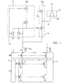
- Figure 1 shows schematically a known reading circuit 10 associated with a bit line of a matrix 11 of non-volatile memory cells having a plurality of bit lines, shown vertically in the drawing, and a plurality of word lines, shown horizontally in the drawing.
- a cell is identified by the intersection of a bit line, indicated BL, with a word line, indicated WL.
- Column decoding circuits, indicated 8, enable one individual bit line to be activated at a time and line decoding circuits, indicated 9, enable one individual word line to be activated at a time. Suitable voltages are thus applied between the electrodes of the memory cell selected at the time in question, for example, the cell indicated 12 in the drawing, by an activated bit line and an activated word line to enable the cell to be read by the circuit 10.
- a reading circuit identical to the circuit 10 is intended to be associated with each of the other bit lines.
- each bit line has a capacitance towards earth (C BL in the drawing) (typically a few pF) which cannot be ignored, the task of the reading circuit is first of all to charge this capacitance rapidly to a predetermined reading voltage level (typically about 1V) and then to detect the presence of a current due to a cell which is conducting, that is, not programmed, or the absence of such a current, which indicates that the cell selected is not conducting, that is, that it is programmed.
- a predetermined reading voltage level typically about 1V
- the circuit 10 is constituted by three main functional blocks: a first block, indicated 14, is constituted essentially by a circuit branch with a controllable switching element which can connect the bit line BL to the positive pole V DD of a voltage supply (the negative pole of which, indicated by the earth symbol, is connected to an electrode of every cell of the memory); a second block, indicated 15, constitutes a driving stage for the switching element and has its output, indicated CAS, connected to the block 14, a first input connected to the bit line BL and a second, enabling input, indicated A, connected to a logic signal generator, not shown; a third comparator and amplifier block 16 has the function of detecting the current flowing through the bit line BL and has a first input connected to the output of the block 14 and a second input RIF connected to a reference voltage source, not shown.
- the output OUT of this block 16 is the output of the reading circuit and is applied to other circuits, not shown, for further amplification of the signal resulting from the reading and for the use thereof, together with other data
- the switching element of the block 14 is constituted by an N-channel field-effect transistor, indicated To with its source connected to the bit line BL and its drain connected to the pole V DD (typically about 4V) of the supply by means of a resistive load constituted by a P-channel transistor T L the gate terminal of which is connected to earth.
- the gate terminal of the transistor To is connected to the output of the driving stage 15.
- the latter is constituted essentially by an inverter formed by two complementary transistors, an N-channel transistor, indicated TNB, connected between the output terminal CAS of the circuit and earth and a P-channel transistor, indicated TPB, connected between the output terminals CAS and the pole V DD by means of another P-channel transistor, indicated TPS.
- the gate terminals of the two transistors of the inverter are joined together at the input of the circuit connected to the bit line BL.
- Another N-channel transistor, indicated TNS, is also connected between the output CAS and earth.
- the gate terminals of the transistors TPS and TNS are joined together at the enabling input A.
- the bit line BL is at substantially zero voltage corresponding to logic level 0 and the enabling terminal A is at a predetermined positive voltage corresponding to logic level 1.
- the transistor TPS is biased so as to be cut off
- the transistor TNS is biased so as to conduct
- the output CAS is at level 0
- the transistor To is biased so as to be cut off. No current flows in the circuit branch of the block 14.
- the enabling terminal A is brought to level 0 so that the transistor TPS becomes conductive and the transistor TNS is cut off. Since the transistor TPB is biased for conduction and the transistor TNB is biased so as to be cut off (because the bit line is still at zero), the voltage at the output CAS rises until the transistor To is made conductive as soon as its threshold voltage is exceeded. A current starts to flow through the branch 14 and rapidly charges the capacitance C BL associated with the bit line and supplies to the input of the comparator 16 a voltage signal, the level of which depends upon the state of the cell selected.
- this level will be higher in the case of a programmed, that is, non-conducting cell, and lower in the case of a non-programmed, that is, conducting cell.
- This signal is compared with the reference signal RIF at the other input of the comparator so that there is a signal corresponding to the state of the cell at the output of the comparator.
- the circuit described above is characterized by a very rapid response, owing to the fact that the inverter of the driving stage and the transistor To are interconnected so as to form a feedback loop.
- This constitutes an advantage when great rapidity of the memory-reading function as a whole is required but may give rise to oscillatory phenomena which often make this advantage useless.
- the working potential (about 1V) for non-volatile memories is normally set very close to the threshold value (about 0.8V) of an N-channel transistor such as the transistor TNB, the sudden transition of the transistor TNB from the cut off state to the conductive state may cause the voltage of the bit line BL to exceed the predetermined optimal working potential and, in some cases, may cause the transistor To to be cut off, even if only briefly.
- the object of the present invention is to provide a circuit for reading a non-volatile memory which does not have the disadvantages of the known circuit described above, that is, in particular, which is not subject to oscillatory phenomena during the charging of the capacitances associated with the bit lines.
- EP-A-0 447 277 discloses a voltage limiter that reduces the voltage excursion of the memory cells' drain.
- Patent Abstract of Japan vol. 17, no. 585 discloses an overcharge preventing circuit that sucks electrons of a switching element control terminal.
- US-A-5,175,705 discloses a discharge circuit connected to the column line to cause the discharge thereof when the potential of the column line is above a predetermined potential.
- EP-A-0 516 225 discloses a circuit comprising a transistor for regulating the drain voltage of a memory cell to be read, and an inverter for driving the regulating transistor, having the same drain voltage as input.
- the circuit according to the invention differs from the known circuit in particular in that it comprises means for reducing the gain in the feedback loop formed by the inverter and the switching transistor To. More particularly, these means are constituted by two additional N-channel transistors with low threshold voltages, indicated Tnat and Tas, the first connected in parallel with the transistor TNB of the inverter, that is, with its source, drain and gate terminals connected to the source, drain and gate terminals of the transistor TNB, respectively, and the second connected like a diode, that is, with its gate terminal joined to its drain terminal, between the source and drain terminals of the transistor TPB of the inverter.
- the two transistors may be of the so-called natural type, that is produced, by the usual technology for manufacturing integrated circuits with non-volatile memories, without the region in which the channel is formed being enriched as is done to increase the threshold voltages of the normal N-channel transistors of the integrated circuit.
- the transistor Tnat starts to conduct before the transistor TNB and this achieves a less abrupt transient of the current output by the driving stage 15 and hence a more gradual transition of the transistor To to the conductive state.
- the transistor Tas has a similar effect, constituting a by-pass for the current between the supply pole V DD and the output terminal of the driving stage, which would otherwise pass solely through the P-channel transistor TPB of the inverter, so that the gain of the inverter is reduced.
- transistor Tnat and the transistor Tas may be used not only together as described but also individually, according to specific requirements, since each of them helps to reduce the gain of the feedback loop independently of the other.
- a further improvement in the performance of the driving stage 15 and hence of the entire reading circuit is achieved by the addition of a P-channel transistor connected like a diode between the drain and source terminals of the N-channel transistor TNB of the inverter.
- This additional transistor, indicated TCL has a higher negative conduction threshold than normal P-channel transistors like the transistor TPB of the inverter and can also easily be formed as a natural transistor in a normal process for the manufacture of integrated circuits with non-volatile memories.
- the transistor TCL starts to conduct as soon as the output voltage of the driving stage exceeds a voltage (about 1.7V) determined by its conduction threshold. This takes place when the transistor To has already started to conduct so that, in short, by creating an additional path for the current towards earth, the transistor TCL acts so as to limit the dynamics of the inverter, that is, it contributes to the reaching of the working level without oscillatory phenomena.
- the detector stage could use a reference voltage derived from the activation of reference cells which do not form part of the memory cells but are structurally equivalent thereto; in this case, the charging of the capacitance of the line which joins the reference cells together as a bit line joins the memory cells together is advantageously carried out by a switching element and with a driver stage which are identical to those described.
- the inverter of the driving stage could be formed with transistors of the same type instead of with complementary transistors.
Landscapes
- Read Only Memory (AREA)
Claims (4)
- Eine Schaltung zum Lesen eines nicht-flüchtigen Speichers, der durch eine Matrix (11) von Zellen mit einer Mehrzahl von Bitleitungen (BL) und von Wortleitungen (WL) gebildet ist, wobei die Schaltung für jede Bitleitung folgende Merkmale aufweist:dadurch gekennzeichnet, daßein steuerbares Schaltelement (To), das ansprechend auf ein Steuersignal, das an einem Steueranschluß desselben anliegt, die Bitleitung (BL) mit einer Spannungsquelle (VDD) verbinden kann;einer Detektorstufe (16), die auf den Fluß von Strom durch die Bitleitung (BL) empfindlich ist; undeiner Treiberstufe (15) mit einem ersten Feldeffekttransistor (TNB), der zwischen ein Massepotential und einen Ausgang (CAS) geschaltet ist, und einem zweiten Feldeffekttransistor (TPB), der zwischen den Ausgang (CAS) und die Spannungsquelle (VDD) geschaltet ist, wobei der erste und der zweite Feldeffekttransistor (TNB, TPB) in der Invertiererkonfiguration verschaltet sind, und wobei der Eingang des Invertierers mit der Bitleitung (BL) und der Ausgang (CAS) des Invertierers mit dem Steueranschluß des steuerbaren Schaltelements (To) verbunden ist,wobei die Treiberstufe (15) eine Einrichtung (Tnat, Tas) zum Reduzieren der Verstärkung der Rückkopplungsschleife aufweist, die durch den Invertierer (TNB, TPB) und durch das steuerbare Schaltelement (To) gebildet wird,
die Einrichtung (Tnat, Tas) zum Reduzieren der Verstärkung einen dritten Feldeffekttransistor (Tnat) aufweist, der einen Leitungsschwellenwert aufweist, der kleiner als derjenige des ersten Transistors (TNB) des Invertierers ist, und der zu dem ersten Transistor (TNB) des Invertierers parallel geschaltet ist und einen Gate-Anschluß aufweist, der mit der Bitleitung (BL) verbunden ist. - Eine Leseschaltung gemäß Anspruch 1, bei der der erste und zweite Transistor (TNB, TPB) von komplementärem Typ sind, wobei die Gate-Anschlüsse derselben an dem Eingang des Invertierers miteinander verbunden sind, und wobei die Drain-Anschlüsse derselben an dem Ausgang (CAS) des Invertierers miteinander verbunden sind, und wobei der dritte Feldeffekttransistor (Tnat) ein N-Kanal-Transistor ist.
- Eine Leseschaltung gemäß Anspruch 2, bei der die Einrichtung (Tnat, Tas) zum Reduzieren der Verstärkung einen N-Kanal-Umleittransistor (Tas) aufweist, der wie eine Diode zwischen den Source- und Drain-Anschluß des zweiten P-Kanal-Transistors (TPB) des Invertierers geschaltet ist.
- Eine Leseschaltung gemäß Anspruch 2 oder 3, bei der die Treiberstufe (15) einen vierten P-Kanal-Transistor (TCL) mit einem negativen Schwellenwert aufweist, der größer als der Schwellenwert des zweiten P-Kanal-Transistors des Invertierers (TPB) ist, und der wie eine Diode zwischen den Drain- und Source-Anschluß des ersten N-Kanal-Transistors des Invertierers geschaltet ist.
Priority Applications (3)
| Application Number | Priority Date | Filing Date | Title |
|---|---|---|---|
| DE69520495T DE69520495T2 (de) | 1995-08-04 | 1995-08-04 | Leseschaltung für nichtflüchtige Speicher |
| EP95830357A EP0757358B1 (de) | 1995-08-04 | 1995-08-04 | Leseschaltung für nichtflüchtige Speicher |
| US08/690,530 US5734610A (en) | 1995-08-04 | 1996-07-31 | Circuit for reading non-volatile memories |
Applications Claiming Priority (1)
| Application Number | Priority Date | Filing Date | Title |
|---|---|---|---|
| EP95830357A EP0757358B1 (de) | 1995-08-04 | 1995-08-04 | Leseschaltung für nichtflüchtige Speicher |
Publications (2)
| Publication Number | Publication Date |
|---|---|
| EP0757358A1 EP0757358A1 (de) | 1997-02-05 |
| EP0757358B1 true EP0757358B1 (de) | 2001-03-28 |
Family
ID=8222001
Family Applications (1)
| Application Number | Title | Priority Date | Filing Date |
|---|---|---|---|
| EP95830357A Expired - Lifetime EP0757358B1 (de) | 1995-08-04 | 1995-08-04 | Leseschaltung für nichtflüchtige Speicher |
Country Status (3)
| Country | Link |
|---|---|
| US (1) | US5734610A (de) |
| EP (1) | EP0757358B1 (de) |
| DE (1) | DE69520495T2 (de) |
Cited By (1)
| Publication number | Priority date | Publication date | Assignee | Title |
|---|---|---|---|---|
| CN101800081B (zh) * | 2009-02-11 | 2012-05-02 | 北京兆易创新科技有限公司 | 一种用于mlc闪存的灵敏放大器和位线快速充电电路 |
Families Citing this family (1)
| Publication number | Priority date | Publication date | Assignee | Title |
|---|---|---|---|---|
| US6788578B1 (en) | 2003-01-27 | 2004-09-07 | Turbo Ic, Inc. | Charge pump for conductive lines in programmable memory array |
Family Cites Families (6)
| Publication number | Priority date | Publication date | Assignee | Title |
|---|---|---|---|---|
| JPH02285593A (ja) * | 1989-04-26 | 1990-11-22 | Mitsubishi Electric Corp | 不揮発性半導体記憶装置 |
| JPH0814996B2 (ja) * | 1989-06-27 | 1996-02-14 | 株式会社東芝 | 半導体記憶装置 |
| FR2659165A1 (fr) * | 1990-03-05 | 1991-09-06 | Sgs Thomson Microelectronics | Memoire ultra-rapide comportant un limiteur de la tension de drain des cellules. |
| IT1249616B (it) * | 1991-05-30 | 1995-03-09 | Sgs Thomson Microelectronics | Circuito di precarica di bit line per la lettura di una cella di memoria eprom. |
| JP3339507B2 (ja) * | 1991-12-17 | 2002-10-28 | 川崎マイクロエレクトロニクス株式会社 | 電流検出型センスアンプ |
| US5487038A (en) * | 1994-08-15 | 1996-01-23 | Creative Integrated Systems, Inc. | Method for read cycle interrupts in a dynamic read-only memory |
-
1995
- 1995-08-04 DE DE69520495T patent/DE69520495T2/de not_active Expired - Fee Related
- 1995-08-04 EP EP95830357A patent/EP0757358B1/de not_active Expired - Lifetime
-
1996
- 1996-07-31 US US08/690,530 patent/US5734610A/en not_active Expired - Lifetime
Cited By (1)
| Publication number | Priority date | Publication date | Assignee | Title |
|---|---|---|---|---|
| CN101800081B (zh) * | 2009-02-11 | 2012-05-02 | 北京兆易创新科技有限公司 | 一种用于mlc闪存的灵敏放大器和位线快速充电电路 |
Also Published As
| Publication number | Publication date |
|---|---|
| US5734610A (en) | 1998-03-31 |
| DE69520495D1 (de) | 2001-05-03 |
| DE69520495T2 (de) | 2001-07-12 |
| EP0757358A1 (de) | 1997-02-05 |
Similar Documents
| Publication | Publication Date | Title |
|---|---|---|
| US5805500A (en) | Circuit and method for generating a read reference signal for nonvolatile memory cells | |
| EP0157905B1 (de) | Halbleiteranordnung | |
| EP0337393B1 (de) | EPROM mit 2 Zellen pro bit | |
| US5699295A (en) | Current detection circuit for reading a memory in integrated circuit form | |
| EP0814483B1 (de) | Leseverfahren und -schaltung für nichtflüchtige Speicherzellen mit Entzerrerschaltung | |
| US4758748A (en) | Sense amplifier for programmable read only memory | |
| EP0225441B1 (de) | Programmierstrom-Steuergerät | |
| US5790466A (en) | Multiple precharging semiconductor memory device | |
| US5303189A (en) | High-speed memory with a limiter of the drain voltage of the cells | |
| US5572465A (en) | Power supply configured sensing scheme for flash EEPROM | |
| US6744673B2 (en) | Feedback biasing integrated circuit | |
| US6400606B1 (en) | Sense amplifier circuit for use in a nonvolatile semiconductor memory device | |
| US4864541A (en) | Integrated circuit of the logic circuit type comprising an electrically programmable non-volatile memory | |
| US5027320A (en) | EPROM circuit having enhanced programmability and improved speed and reliability | |
| US4388541A (en) | Circuit arrangement with MOS-transistors for the rapid evaluation of the logic state of a sampling node | |
| US4290119A (en) | Memory device protected against undesirable supply voltage level | |
| JPH0323997B2 (de) | ||
| US7397702B2 (en) | Read/verify circuit for multilevel memory cells with ramp read voltage, and read/verify method thereof | |
| US6392447B2 (en) | Sense amplifier with improved sensitivity | |
| US4709352A (en) | MOS read-only memory systems | |
| US6175521B1 (en) | Voltage regulator for programming electrically programmable non-volatile memory cells in a cell matrix | |
| US5719490A (en) | Dual sourced voltage supply circuit | |
| US5734610A (en) | Circuit for reading non-volatile memories | |
| US5666310A (en) | High-speed sense amplifier having variable current level trip point | |
| WO2001057874A2 (en) | Voltage boost level clamping circuit for a flash memory |
Legal Events
| Date | Code | Title | Description |
|---|---|---|---|
| PUAI | Public reference made under article 153(3) epc to a published international application that has entered the european phase |
Free format text: ORIGINAL CODE: 0009012 |
|
| AK | Designated contracting states |
Kind code of ref document: A1 Designated state(s): DE FR GB IT |
|
| 17P | Request for examination filed |
Effective date: 19970709 |
|
| RAP3 | Party data changed (applicant data changed or rights of an application transferred) |
Owner name: STMICROELECTRONICS S.R.L. |
|
| 17Q | First examination report despatched |
Effective date: 19990602 |
|
| GRAG | Despatch of communication of intention to grant |
Free format text: ORIGINAL CODE: EPIDOS AGRA |
|
| GRAG | Despatch of communication of intention to grant |
Free format text: ORIGINAL CODE: EPIDOS AGRA |
|
| GRAH | Despatch of communication of intention to grant a patent |
Free format text: ORIGINAL CODE: EPIDOS IGRA |
|
| ITF | It: translation for a ep patent filed | ||
| GRAH | Despatch of communication of intention to grant a patent |
Free format text: ORIGINAL CODE: EPIDOS IGRA |
|
| GRAA | (expected) grant |
Free format text: ORIGINAL CODE: 0009210 |
|
| AK | Designated contracting states |
Kind code of ref document: B1 Designated state(s): DE FR GB IT |
|
| REF | Corresponds to: |
Ref document number: 69520495 Country of ref document: DE Date of ref document: 20010503 |
|
| ET | Fr: translation filed | ||
| REG | Reference to a national code |
Ref country code: GB Ref legal event code: IF02 |
|
| PLBE | No opposition filed within time limit |
Free format text: ORIGINAL CODE: 0009261 |
|
| STAA | Information on the status of an ep patent application or granted ep patent |
Free format text: STATUS: NO OPPOSITION FILED WITHIN TIME LIMIT |
|
| 26N | No opposition filed | ||
| PGFP | Annual fee paid to national office [announced via postgrant information from national office to epo] |
Ref country code: DE Payment date: 20040812 Year of fee payment: 10 |
|
| PG25 | Lapsed in a contracting state [announced via postgrant information from national office to epo] |
Ref country code: IT Free format text: LAPSE BECAUSE OF NON-PAYMENT OF DUE FEES;WARNING: LAPSES OF ITALIAN PATENTS WITH EFFECTIVE DATE BEFORE 2007 MAY HAVE OCCURRED AT ANY TIME BEFORE 2007. THE CORRECT EFFECTIVE DATE MAY BE DIFFERENT FROM THE ONE RECORDED. Effective date: 20050804 |
|
| PG25 | Lapsed in a contracting state [announced via postgrant information from national office to epo] |
Ref country code: DE Free format text: LAPSE BECAUSE OF NON-PAYMENT OF DUE FEES Effective date: 20060301 |
|
| PGFP | Annual fee paid to national office [announced via postgrant information from national office to epo] |
Ref country code: FR Payment date: 20080828 Year of fee payment: 14 |
|
| PGFP | Annual fee paid to national office [announced via postgrant information from national office to epo] |
Ref country code: GB Payment date: 20080729 Year of fee payment: 14 |
|
| GBPC | Gb: european patent ceased through non-payment of renewal fee |
Effective date: 20090804 |
|
| REG | Reference to a national code |
Ref country code: FR Ref legal event code: ST Effective date: 20100430 |
|
| PG25 | Lapsed in a contracting state [announced via postgrant information from national office to epo] |
Ref country code: FR Free format text: LAPSE BECAUSE OF NON-PAYMENT OF DUE FEES Effective date: 20090831 |
|
| PG25 | Lapsed in a contracting state [announced via postgrant information from national office to epo] |
Ref country code: GB Free format text: LAPSE BECAUSE OF NON-PAYMENT OF DUE FEES Effective date: 20090804 |