EP0222338B1 - Halbleiterphotoempfindliche Vorrichtung - Google Patents
Halbleiterphotoempfindliche Vorrichtung Download PDFInfo
- Publication number
- EP0222338B1 EP0222338B1 EP19860115449 EP86115449A EP0222338B1 EP 0222338 B1 EP0222338 B1 EP 0222338B1 EP 19860115449 EP19860115449 EP 19860115449 EP 86115449 A EP86115449 A EP 86115449A EP 0222338 B1 EP0222338 B1 EP 0222338B1
- Authority
- EP
- European Patent Office
- Prior art keywords
- light
- sensing device
- semiconductor
- substrate
- shading
- Prior art date
- Legal status (The legal status is an assumption and is not a legal conclusion. Google has not performed a legal analysis and makes no representation as to the accuracy of the status listed.)
- Expired
Links
- 239000004065 semiconductor Substances 0.000 title claims description 64
- 239000000758 substrate Substances 0.000 claims description 31
- 229910052782 aluminium Inorganic materials 0.000 claims description 7
- XAGFODPZIPBFFR-UHFFFAOYSA-N aluminium Chemical compound [Al] XAGFODPZIPBFFR-UHFFFAOYSA-N 0.000 claims description 6
- 238000006243 chemical reaction Methods 0.000 claims description 5
- 229910052710 silicon Inorganic materials 0.000 claims description 5
- 239000010703 silicon Substances 0.000 claims description 5
- 230000000873 masking effect Effects 0.000 claims description 3
- 239000004411 aluminium Substances 0.000 claims 1
- 230000002093 peripheral effect Effects 0.000 claims 1
- 238000010521 absorption reaction Methods 0.000 description 8
- 230000003071 parasitic effect Effects 0.000 description 6
- XUIMIQQOPSSXEZ-UHFFFAOYSA-N Silicon Chemical compound [Si] XUIMIQQOPSSXEZ-UHFFFAOYSA-N 0.000 description 4
- 239000013078 crystal Substances 0.000 description 4
- 230000000694 effects Effects 0.000 description 4
- 238000009413 insulation Methods 0.000 description 3
- 239000000463 material Substances 0.000 description 3
- 239000003463 adsorbent Substances 0.000 description 2
- 239000000969 carrier Substances 0.000 description 2
- 238000010438 heat treatment Methods 0.000 description 2
- 238000004519 manufacturing process Methods 0.000 description 2
- 238000000034 method Methods 0.000 description 2
- GPXJNWSHGFTCBW-UHFFFAOYSA-N Indium phosphide Chemical compound [In]#P GPXJNWSHGFTCBW-UHFFFAOYSA-N 0.000 description 1
- 239000004642 Polyimide Substances 0.000 description 1
- 238000004891 communication Methods 0.000 description 1
- 230000008021 deposition Effects 0.000 description 1
- 238000010586 diagram Methods 0.000 description 1
- 238000009792 diffusion process Methods 0.000 description 1
- 229910052732 germanium Inorganic materials 0.000 description 1
- GNPVGFCGXDBREM-UHFFFAOYSA-N germanium atom Chemical compound [Ge] GNPVGFCGXDBREM-UHFFFAOYSA-N 0.000 description 1
- 230000007257 malfunction Effects 0.000 description 1
- 238000000465 moulding Methods 0.000 description 1
- 230000003287 optical effect Effects 0.000 description 1
- 239000013307 optical fiber Substances 0.000 description 1
- 229920001721 polyimide Polymers 0.000 description 1
- 230000001105 regulatory effect Effects 0.000 description 1
Images


Classifications
-
- H—ELECTRICITY
- H03—ELECTRONIC CIRCUITRY
- H03F—AMPLIFIERS
- H03F3/00—Amplifiers with only discharge tubes or only semiconductor devices as amplifying elements
- H03F3/04—Amplifiers with only discharge tubes or only semiconductor devices as amplifying elements with semiconductor devices only
- H03F3/08—Amplifiers with only discharge tubes or only semiconductor devices as amplifying elements with semiconductor devices only controlled by light
-
- H—ELECTRICITY
- H01—ELECTRIC ELEMENTS
- H01L—SEMICONDUCTOR DEVICES NOT COVERED BY CLASS H10
- H01L27/00—Devices consisting of a plurality of semiconductor or other solid-state components formed in or on a common substrate
- H01L27/14—Devices consisting of a plurality of semiconductor or other solid-state components formed in or on a common substrate including semiconductor components sensitive to infrared radiation, light, electromagnetic radiation of shorter wavelength or corpuscular radiation and specially adapted either for the conversion of the energy of such radiation into electrical energy or for the control of electrical energy by such radiation
- H01L27/144—Devices controlled by radiation
- H01L27/1443—Devices controlled by radiation with at least one potential jump or surface barrier
-
- H—ELECTRICITY
- H01—ELECTRIC ELEMENTS
- H01L—SEMICONDUCTOR DEVICES NOT COVERED BY CLASS H10
- H01L31/00—Semiconductor devices sensitive to infrared radiation, light, electromagnetic radiation of shorter wavelength or corpuscular radiation and specially adapted either for the conversion of the energy of such radiation into electrical energy or for the control of electrical energy by such radiation; Processes or apparatus specially adapted for the manufacture or treatment thereof or of parts thereof; Details thereof
- H01L31/02—Details
- H01L31/0216—Coatings
- H01L31/02161—Coatings for devices characterised by at least one potential jump barrier or surface barrier
- H01L31/02162—Coatings for devices characterised by at least one potential jump barrier or surface barrier for filtering or shielding light, e.g. multicolour filters for photodetectors
- H01L31/02164—Coatings for devices characterised by at least one potential jump barrier or surface barrier for filtering or shielding light, e.g. multicolour filters for photodetectors for shielding light, e.g. light blocking layers, cold shields for infrared detectors
Definitions
- the present invention relates to a photo-sensing device, and more particularly to a semiconductor photo-sensing device suitably adapted to photoelectric switches, optical fiber data links, high speed optical communication, etc.
- Previously known semiconductor photo-sensing devices are provided with a photosensor for photo-electric conversion and an amplifier circuit for amplifying the output from the photosensor.
- the photosensor is constructed by a PN-junction diode, for example while the amplifier circuit is constructed by bipolar transistors, diodes, resistors, etc., for example.
- circuit components or elements are integrated in a single semiconductor chip in the prior art monolithic semiconductor photo-sensing device as shown in Figs. 1A and 1B. These circuit elements are formed in the semiconductor substrate 10 through diffusion techniques, and are interconnected by wiring layers. The surface of the semiconductor substrate 10 is entirely covered with an insulating film 12 which is capable of transmitting a light having a desired wavelength, and the wiring layers are disposed in the insulating film 12 in contact with the circuit elements.
- the PN-junction diode employs a photocurrent which will flow when a light is emitted to the vicinity of the PN-junction thereof.
- a photocurrent would flow through the PN-junctions between the base and collector and between the emitter and base.
- the photocurrent flowing in the amplifier circuit gives rise to noise or malfunction when the amplifier circuit is in operation.
- the prior art photo-sensing device is provided with a light-shading layer 14, e.g., aluminum, as shown in Figs. 1A and 1B.
- Layer 14 is formed on substantially the whole surface of the insulating film 12 except the portions corresponding to a light receiving region 16 of the photosensor and a bonding region 18, thereby entirely masking the amplifier circuit.
- a semiconductor device of this kind is also known from JP-A-60-177 685.
- the insulating film 12 may contain pinholes on the circuit elements or wiring layers. In this case, the portions associated with the pinholes remain exposed. Therefore, if aluminum is vacuum-deposited on the insulating layer 12 for the provision of the light-shading layer 14, the aluminum will be also deposited on the exposed portions of the circuit elements or wiring layers through the pinholes. Thus, these exposed portions will be disadvantageously communicated or short-circuited with each other by the light-shading layer 14.
- both the light-shading layer 14 and the wiring layers are electrically conductive, and are adjacent to each other through the insulating layer 12. Therefore, each of the wiring layers is capacitively coupled with the light-shading layer to provide the parasitic capacitance therebetween. This parasitic capacitance will lead to the noise at a noticeable level in the operation of the amplifier circuit.
- the moisture contained in the insulating layer 12 will be vaporized due to the heat applied during the heat treatment after the aluminum deposition, e.g., molding process, and will be stored as bubbles within the insulating film 12 covered with the light-shading layer 14. Therefore, a relatively large force will be applied to portions of the wiring layers and light-shading layer 14, thus deforming them. Accordingly, some disconnections may occur in the wiring layers and/or poor insulation may result between the wiring layers and the light-shading layer 14. This inconvenience is more liable to occur than the inconveniences resulting from the pinholes and parasitic capacitances and so it is most critical.
- the insulating layer 12 is configured in a multi-layer structure, in which one layer is made of a highly adsorbent material such as polyimide, it has been confirmed by the inventor of the present invention that the inconvenience due to the presence of the bubbles occurs in many cases. It has been also confirmed that the disconnections and poor insulation are liable to occur below the center portion of the light-shading layer 14.
- An object of the present invention is to provide a semiconductor photo-sensing device which is capable of providing a higher production yield and sufficient operation reliability.
- a semiconductor photo-sensing device comprising a substrate means, a photo-sensor means for photoelectric conversion, a plurality of processing means formed in the substrate means for cooperatively processing an output signal of the photosensor means and containing at least one PN-junction, an insulative light-transmission film formed on the substrate means and a light-shading layer formed on the insulative film for masking the restricted areas corresponding to the respective processing means and a miniumum of their neighboring areas.
- the light-shading layer is not formed on substantially the whole surface of the insulating film, but on a comparatively small area thereof, enough to mask only the regions where the processing sections are formed and their neighboring areas. Therefore, even if the insulating film is highly adsorbent, the moisture contained in the insulating film is not stored as bubbles below the center portion of the light-shading layer during the heat treatment, but can be sufficiently emitted, externally. The occurrence of the inconvenience resulting from the pinholes and parasitic capacitances can be also minimized, since the area of the light-shading layer is minimized in an allowable range.
- this photo-sensing device includes a photo-sensor 20 for photo-electric conversion and an amplifier circuit 22 for amplifying the output signal from the photosensor 20.
- the photosensor 20 is constructed by a diode 20A which can efficiently photoelectrically convert the light having a desired wavelength, e.g., infrared light having a wavelength of 940 nm.
- the amplifier circuit 22 is constructed by a voltage regulator 22A, amplifier 22B, Schmitt circuit 22C, load resistor 22D and output transistor 22E, for example.
- the semiconductor photo-sensing device operates as follows.
- a power source voltage is applied between terminals Vcc and GND and stabilized by the voltage regulator 22A.
- the diode 20A generates an electric signal in accordance with the intensity of an incident light.
- This electric signal is amplified by the amplifier 22B, and is supplied as a voltage signal to the Schmitt circuit 22C.
- the Schmitt circuit 22C compares the level of the supplied voltage signal with a reference voltage level and controls the conduction state of the output transistor 22E in accordance with the level difference.
- the voltage at an output terminal OUT is set to a low level when the transistor 22E is turned on, and set to a high level when the transistor 22E is turned off. This means that a digital signal is produced from the output terminal OUT.
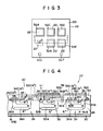
- the photosensor 20 and amplifier circuit 22 that is, the diode 20A, voltage regulator 22A, amplifier 22B, Schmitt circuit 22C, load resistor 22D and output transistor 22E are arranged in a single semiconductor chip as shown in Fig. 3.
- the photosensor 20 has a vertical NPN transistor 24 as shown in Fig. 4 to provide the diode 20A.
- the transistor 24 has an N+-type region 24A buried within a P-type silicon substrate 26 and an N-type region 24B which is formed, in contact with the region 24A, in the surface area of the substrate 26.
- the transistor 24 has also a P+-type region 24C and N+-type region 24D which are formed in the surface area of the region 24B, and an N+-type region 24E which is formed in the surface area of the region 24C.
- a conductive layer, e.g., aluminum Al layer 28 is formed on the regions 24B, 24C, 24D and substrate 26.
- the Al layer 28 serves as an anode electrode and a wiring layer.
- the regions 24B and 24C are short-circuited through the region 24D and Al layer 28.
- An Al layer 30 is formed on the bottom surface of the substrate 26, and serves as a terminal GND.
- the PN-junction between the regions 24C and 24E and its neighborhood are used as a light-receiving portion of the diode 20A.
- the amplifier circuit 22 has vertical NPN transistors 32 and 34 as shown in Fig. 4 to provide the amplifier 22B and output transistor 22E.
- the transistor 32 is manufactured in the same manner as the transistor 24, and has an N+-type region 32A, N-type region 32B, P+-type region 32C, N+-type region 32D and N+-type region 32E.
- An Al layer 35 is formed on the region 24E as a cathode electrode of the diode 24 and formed on the region 32C as a base electrode of the transistor 32; these regions 24C and 32 are connected with each other through the Al layer 35.
- An Al layer 36 is formed on the region 32D as a collector electrode of the transistor 32, and receives a regulated power voltage V1 from voltage regulator 22A.
- Al layer 38 is formed on the region 32E as an emitter electrode of the transistor 32, and also contacts with a P+-type region formed in the surface area of the substrate 26.
- the transistor 34 like the transistor 32, has N+-type regions 34A, 34D and 34E, an N-type region 34B and a P+-type region 34C.
- Al layers 42A, 42B and 42C are formed in contact with the regions 34D, 34C and 34E, respectively.
- an insulating film 50 is formed on the substrate 26 and transistors 24, 32 and 34.
- This insulating film 50 serves to electrically insulate the Al layers from one another and also to permit the light to be transmitted.
- light-shading layers 52A to 52E of e.g. Al are formed on the insulating film 50, and mask the areas where the voltage regulator 22A, amplifier 22B, Schmitt circuit 22c, load resistor 22D and output transistor 22E are formed, and their neighboring areas.
- the areas of the light-shading layers 52A to 52E are defined so that the amount of light incident on the PN-junctions and their neighboring area can be made as little as possible within the range of not invalidating the circuit operation of the photo-sensing device. This will be explained in more detail hereinbelow.
- the light When a semiconductor crystal receives a light, the light can penetrate in the crystal by the depth L ⁇ (referred to as an absorption length).
- the infrared light having a wavelength of 940 nm (0.94 ⁇ m) is emitted to the silicon substrate 26, as shown in Figs. 3 and 4, from the infrared diode serving as a light source.
- the absorption coefficient ⁇ o is approximately 2 ⁇ 102 cm ⁇ 1 as seen from Fig.
- the absorption length L ⁇ as defined above means a distance when the intensity of the incident light is reduced to 1/e (e:exponential 2.718 ...) thereof, approximately 37 % of the incident light will reach the PN-junction. Therefore, in order to sufficiently eliminate the noise due to the incident light, the thickness of the depletion layer along a PN-junction, the width of the diffused region must be considered. When the light is emitted to the PN-junction between the regions 34C and 34B, some carriers will be produced. The carriers will be amplified because of the amplifying operation of the transistor 34 to create noticeable noise.
- the distance from the edge of the light-shading layer 52E to the outermost PN-junction of the transistor 34 is ⁇ 2
- ⁇ 2 must also be set to a value of 50 ⁇ m or more.
- the light-shading layer 52E is made apart from the PN-junction between the region 34B and the substrate 26 by 50 ⁇ m or more.
- the other light-shading layers 52A to 52D are also made apart from the outermost PN-junctions of the associated semiconductor elements by 5 ⁇ m or more.
- the region for which the light-shading is to be performed is minimized, the area of the light-shading layers can be sufficiently reduced as compared with the prior art semiconductor photo-sensing device.
- the possibility of producing short-circuiting among the wiring layers due to the presence of pinholes can be minimized.
- the noise resulting from the parasitic capacitances between the light-shading layers and the wiring layers can also be minimized.
- the disconnections in the wiring layers and poor insulation between the wiring layers and light shading-layers, which are produced due to the moisture contained in the insulating layer can be efficiently reduced.
- the reduction of the area of the light-shading layers assures that the moisture, when vaporized, can easily emit externally so that it is not stored as bubbles between the light-shading layers and the insulating film. Accordingly, the reliability of the semiconductor photo-sensing device according to this embodiment can be greatly improved.
- a silicon substrate 26 was employed but the semiconductor substrate of other materials can also be employed.
- the wavelength of incident light is varied, it is only necessary to change the thickness of the insulating layer 50 and the pattern, size, etc. of each of the light-shading layers 52A to 52E.
- the photo-diode 20A was constructed by the NPN transistor 24 with its base and collector short-circuited, it can be constructed by an ordinary PN-junction photodiode.
- Fig. 6 shows a planar structure of the semiconductor photo-sensing device according to a second embodiment of the present invention.
- This device is the same as the device according to the first embodiment except that the light-shading layers 52A to 52E are connected with one another through a connection layer 60 of the same material, i.e., Al, as the light-shading layers and are grounded.
- the circuit structure of the device according to this embodiment is equivalent to that of the device according to the first embodiment as shown in Fig. 2 although the arrangement of the photosensor 20 and amplifier circuit 22 in this embodiment is different from the first embodiment as shown in Fig. 3.
- the device according to this embodiment can provide a more improved electromagnetic shielding effect.
- Fig. 7 shows a planar structure of the semiconductor photo-sensing device according to a third embodiment of the present invention.
- This device is the same as the device according to the second embodiment except that the photosensor 20 and amplifier circuit 22 are formed in individual first and second semiconductor chips, respectively, which are connected with each other through their associated bonding pads 66A and 66B and are grounded.
- the circuit structure of the amplifier circuit 22 in this embodiment is equivalent to that as shown in Fig. 2, both the load resistor 22D and output transistor 22E, for example, are masked by a common light-shading layer 64.
- the device according to this embodiment can provide the same effect as the second embodiment.
- Fig. 8 shows a planar structure of the semiconductor photo-sensing device according to a fourth embodiment of the present invention.
- This device is the same as the device according to the second embodiment except that the photosensor 20 and a part of the amplifier circuit 22, e.g., the amplifier 22B, are formed in a first individual semiconductor chip while the remaining part of the amplifier circuit 22 is formed in a second individual semiconductor chip; the first and second semiconductor chips are connected with each other through their associated bonding pads 66A, 66B, 66C and 66D and are grounded.
- the device according to this embodiment can provide the same effect as the second embodiment.
Claims (13)
- Lichtempfindliche Halbleitervorrichtung, die folgende Mittel aufweist:- Substratmittel (26);- Lichtsensormittel (20) für die lichtelektrische Umwandlung;- Verarbeitungsmittel (22) zur Verarbeitung eines Ausgangssignals der Lichtsensormittel (20), wobei erstere in den Substratmitteln (26) ausgebildet sind und mindestens einen einzelnen PN-Übergang aufweisen;- einen lichtdurchlässigen Isolierfilm (50) auf den Substratmitteln (26); und- Lichtabschirmmittel (52A-52E) auf dem lichtdurchlässigen Film,dadurch gekennzeichnet, daß die Lichtabschirmmittel (52A-52E) nur einen Bereich maskieren, der den Verarbeitungsmitteln (22) und einem Minimum ihrer benachbarten Bereiche entspricht, wobei das Minimum so festgesetzt ist, daß der Betrieb der Verarbeitungsmittel (22) nicht durch einfallendes Licht unwirksam gemacht wird.
- Lichtempfindliche Halbleitervorrichtung nach Anspruch 1,
dadurch gekennzeichnet, daß die Verarbeitungsmittel aus einer Vielzahl von Verarbeitungsabschnitten (22A-22E9 zur kooperativen Verarbeitung eines Ausgangssignals der Lichtsensormittel (20) bestehen, wobei jeder der Verarbeitungsabschnitte (22A-22E) mindestens einen einzelnen PN-Übergang aufweist. - Lichtempfindliche Halbleitervorrichtung nach Anspruch 2,
dadurch gekennzeichnet, daß die Lichtabschirmmittel eine Vielzahl von Lichtabschirmschichten (52A-52E) zum Maskieren der begrenzten Bereiche entsprechend den jeweiligen Verarbeitungsabschnitten (22A-22E) und ihrer benachbarten Bereiche aufweisen. - Lichtempfindliche Halbleitervorrichtung nach Anspruch 3,
dadurch gekennzeichnet, daß jede der lichtabschirmenden Schichten (52A-52E) leitend und mit Erde verbunden ist. - Lichtempfindliche Halbleitervorrichtung nach Anspruch 4,
dadurch gekennzeichnet, daß die lichtabschirmenden Mittel weiter mindestens eine leitende Leitung (60) zum Anschließen der lichtabschirmenden Schichten (52A-52E) in Reihenschaltung aufweisen. - Lichtempfindliche Halbleitervorrichtung nach Anspruch 5,
dadurch gekennzeichnet, daß die lichtabschirmenden Schichten (52A-52E) sowie die leitende Leitung (60) aus Aluminium bestehen. - Lichtempfindliche Halbleitervorrichtung nach Anspruch 1,
dadurch gekennzeichnet, daß die Substratmittel aus einem einzelnen Halbleitersubstrat (26) bestehen, wobei die lichtempfindlichen Mittel (20) und die Verarbeitungsmittel (22) im Halbleitersubstrat (26) ausgebildet sind. - Lichtempfindliche Halbleitervorrichtung nach Anspruch 1,
dadurch gekennzeichnet, daß die Halbleitermittel aus einem ersten und einem zweiten Halbleitersubstrat bestehen, wobei die lichtempfindlichen Mittel (20) im ersten Halbleitersubstrat und die Verarbeitungsmittel (22) im zweiten Halbleitersubstrat ausgebildet sind. - Lichtempfindliche Halbleitervorrichtung nach Anspruch 1,
dadurch gekennzeichnet, daß die Substratmittel aus einem ersten und einem zweiten Halbleitersubstrat bestehen, wobei die lichtempfindlichen Mittel (20) sowie ein Teil der Verarbeitungsmittel (22) im ersten Halbleitersubstrat, und der restliche Teil der Verarbeitungsmittel (22) im zweiten Halbleitersubstrat ausgebildet ist. - Lichtempfindliche Halbleitervorrichtung nach Anspruch 1,
dadurch gekennzeichnet, daß die Verarbeitungsmittel als Verstärkerschaltung (22) ausgebildet sind. - Lichtempfindliche Halbleitervorrichtung nach Anspruch 2,
dadurch gekennzeichnet, daß mindestens einer der Verarbeitungsabschnitte (22A-22E) einen Bipolartransistor aufweist. - Lichtempfindliche Halbleitervorrichtung nach Anspruch 1,
dadurch gekennzeichnet, daß die lichtabschirmenden Mittel (52A-52E) über die Verarbeitungsmittel (22) geschichtet sind, wobei eine Umfangskante zum äußersten PN-Übergang der Verarbeitungsmittel (22) einen vorbestimmten Abstand einhält. - Lichtempfindliche Halbleitervorrichtung nach Anspruch 12,
dadurch gekennzeichnet, daß die Substratmittel (26) aus Silicium bestehen und der vorbestimmte Abstand mindestens 50 µm beträgt.
Applications Claiming Priority (2)
| Application Number | Priority Date | Filing Date | Title |
|---|---|---|---|
| JP60253211A JPS62112382A (ja) | 1985-11-12 | 1985-11-12 | 半導体受光装置 |
| JP253211/85 | 1985-11-12 |
Publications (3)
| Publication Number | Publication Date |
|---|---|
| EP0222338A2 EP0222338A2 (de) | 1987-05-20 |
| EP0222338A3 EP0222338A3 (en) | 1989-02-08 |
| EP0222338B1 true EP0222338B1 (de) | 1992-04-15 |
Family
ID=17248099
Family Applications (1)
| Application Number | Title | Priority Date | Filing Date |
|---|---|---|---|
| EP19860115449 Expired EP0222338B1 (de) | 1985-11-12 | 1986-11-07 | Halbleiterphotoempfindliche Vorrichtung |
Country Status (3)
| Country | Link |
|---|---|
| EP (1) | EP0222338B1 (de) |
| JP (1) | JPS62112382A (de) |
| DE (1) | DE3684873D1 (de) |
Families Citing this family (6)
| Publication number | Priority date | Publication date | Assignee | Title |
|---|---|---|---|---|
| US5352920A (en) * | 1988-06-06 | 1994-10-04 | Canon Kabushiki Kaisha | Photoelectric converter with light shielding sections |
| US5410179A (en) * | 1990-04-05 | 1995-04-25 | Martin Marietta Corporation | Microwave component having tailored operating characteristics and method of tailoring |
| JPH05304280A (ja) * | 1992-04-27 | 1993-11-16 | Mitsubishi Electric Corp | 半導体集積回路装置 |
| US6278169B1 (en) * | 1998-05-07 | 2001-08-21 | Analog Devices, Inc. | Image sensor shielding |
| EP1176808A3 (de) | 2000-07-27 | 2003-01-02 | Canon Kabushiki Kaisha | Bildaufnahmevorrichtung |
| JP6693068B2 (ja) * | 2015-03-12 | 2020-05-13 | ソニー株式会社 | 固体撮像装置および製造方法、並びに電子機器 |
Family Cites Families (5)
| Publication number | Priority date | Publication date | Assignee | Title |
|---|---|---|---|---|
| JPS57145368A (en) * | 1981-03-04 | 1982-09-08 | Hitachi Ltd | Semiconductor intergrated circuit |
| JPS5980964A (ja) * | 1982-11-01 | 1984-05-10 | Toshiba Corp | 光電変換素子 |
| JPS59134872A (ja) * | 1983-01-23 | 1984-08-02 | Rohm Co Ltd | フオトセンサ−用ic |
| FR2557371B1 (fr) * | 1983-12-27 | 1987-01-16 | Thomson Csf | Dispositif photosensible comportant entre les detecteurs des zones opaques au rayonnement a detecter, et procede de fabrication |
| JPS60177685A (ja) * | 1984-02-23 | 1985-09-11 | Sumitomo Electric Ind Ltd | 半導体装置 |
-
1985
- 1985-11-12 JP JP60253211A patent/JPS62112382A/ja active Pending
-
1986
- 1986-11-07 DE DE8686115449T patent/DE3684873D1/de not_active Expired - Lifetime
- 1986-11-07 EP EP19860115449 patent/EP0222338B1/de not_active Expired
Also Published As
| Publication number | Publication date |
|---|---|
| JPS62112382A (ja) | 1987-05-23 |
| EP0222338A3 (en) | 1989-02-08 |
| DE3684873D1 (de) | 1992-05-21 |
| EP0222338A2 (de) | 1987-05-20 |
Similar Documents
| Publication | Publication Date | Title |
|---|---|---|
| US5994204A (en) | Silicon-glass bonded wafers | |
| US5128729A (en) | Complex opto-isolator with improved stand-off voltage stability | |
| US5726500A (en) | Semiconductor hybrid component | |
| US3486029A (en) | Radiative interconnection arrangement | |
| JPH0467789B2 (de) | ||
| US4318115A (en) | Dual junction photoelectric semiconductor device | |
| US5357121A (en) | Optoelectronic integrated circuit | |
| EP0019234A1 (de) | Aufbau einer integrierten Halbleiterschaltung | |
| JP2004119713A (ja) | 半導体光センサ装置 | |
| EP0222338B1 (de) | Halbleiterphotoempfindliche Vorrichtung | |
| US5410168A (en) | Infrared imaging device | |
| US4920395A (en) | High sensitivity photodiode | |
| US4183034A (en) | Pin photodiode and integrated circuit including same | |
| EP0835528B1 (de) | Monolithischer linearer optokoppler | |
| US4649409A (en) | Photoelectric transducer element | |
| US4903103A (en) | Semiconductor photodiode device | |
| US20030173569A1 (en) | Receiving optics and photosemiconductor device having the same | |
| US6989522B2 (en) | Light-receiving module and light-receiving device having malfunction preventing structure | |
| US5583072A (en) | Method of manufacturing a monolithic linear optocoupler | |
| JP3855351B2 (ja) | 光センサ | |
| JPH07120761B2 (ja) | 受光素子内蔵型半導体集積回路 | |
| JP2770810B2 (ja) | 受光素子 | |
| JP3497977B2 (ja) | 受光素子およびこれを用いた光結合装置 | |
| US5142342A (en) | Optocoupler | |
| JP3794606B2 (ja) | 受光素子用接合容量 |
Legal Events
| Date | Code | Title | Description |
|---|---|---|---|
| PUAI | Public reference made under article 153(3) epc to a published international application that has entered the european phase |
Free format text: ORIGINAL CODE: 0009012 |
|
| 17P | Request for examination filed |
Effective date: 19861107 |
|
| AK | Designated contracting states |
Kind code of ref document: A2 Designated state(s): DE FR GB |
|
| PUAL | Search report despatched |
Free format text: ORIGINAL CODE: 0009013 |
|
| AK | Designated contracting states |
Kind code of ref document: A3 Designated state(s): DE FR GB |
|
| 17Q | First examination report despatched |
Effective date: 19900827 |
|
| GRAA | (expected) grant |
Free format text: ORIGINAL CODE: 0009210 |
|
| AK | Designated contracting states |
Kind code of ref document: B1 Designated state(s): DE FR GB |
|
| REF | Corresponds to: |
Ref document number: 3684873 Country of ref document: DE Date of ref document: 19920521 |
|
| ET | Fr: translation filed | ||
| PLBE | No opposition filed within time limit |
Free format text: ORIGINAL CODE: 0009261 |
|
| STAA | Information on the status of an ep patent application or granted ep patent |
Free format text: STATUS: NO OPPOSITION FILED WITHIN TIME LIMIT |
|
| 26N | No opposition filed | ||
| PGFP | Annual fee paid to national office [announced via postgrant information from national office to epo] |
Ref country code: GB Payment date: 19971029 Year of fee payment: 12 |
|
| PGFP | Annual fee paid to national office [announced via postgrant information from national office to epo] |
Ref country code: FR Payment date: 19971112 Year of fee payment: 12 |
|
| PG25 | Lapsed in a contracting state [announced via postgrant information from national office to epo] |
Ref country code: GB Free format text: LAPSE BECAUSE OF NON-PAYMENT OF DUE FEES Effective date: 19981107 |
|
| GBPC | Gb: european patent ceased through non-payment of renewal fee |
Effective date: 19981107 |
|
| PG25 | Lapsed in a contracting state [announced via postgrant information from national office to epo] |
Ref country code: FR Free format text: LAPSE BECAUSE OF NON-PAYMENT OF DUE FEES Effective date: 19990730 |
|
| REG | Reference to a national code |
Ref country code: FR Ref legal event code: ST |
|
| PGFP | Annual fee paid to national office [announced via postgrant information from national office to epo] |
Ref country code: DE Payment date: 20051103 Year of fee payment: 20 |