EP0220503B1 - Procédé et structure pour permettre un changement voulu dans un ensemble de dispositifs modulaires - Google Patents
Procédé et structure pour permettre un changement voulu dans un ensemble de dispositifs modulaires Download PDFInfo
- Publication number
- EP0220503B1 EP0220503B1 EP86113233A EP86113233A EP0220503B1 EP 0220503 B1 EP0220503 B1 EP 0220503B1 EP 86113233 A EP86113233 A EP 86113233A EP 86113233 A EP86113233 A EP 86113233A EP 0220503 B1 EP0220503 B1 EP 0220503B1
- Authority
- EP
- European Patent Office
- Prior art keywords
- engineering change
- solder pads
- substrate
- pads
- lines
- Prior art date
- Legal status (The legal status is an assumption and is not a legal conclusion. Google has not performed a legal analysis and makes no representation as to the accuracy of the status listed.)
- Expired - Lifetime
Links
- 238000000034 method Methods 0.000 title claims description 23
- 239000000758 substrate Substances 0.000 claims description 77
- 229910000679 solder Inorganic materials 0.000 claims description 66
- 238000005272 metallurgy Methods 0.000 claims description 26
- 239000010410 layer Substances 0.000 claims description 15
- 238000001465 metallisation Methods 0.000 claims description 14
- 239000002184 metal Substances 0.000 claims description 6
- 229910052751 metal Inorganic materials 0.000 claims description 6
- 238000005304 joining Methods 0.000 claims description 5
- 239000000919 ceramic Substances 0.000 claims description 4
- 239000004065 semiconductor Substances 0.000 claims description 3
- 239000002356 single layer Substances 0.000 claims description 2
- 239000003989 dielectric material Substances 0.000 claims 2
- 239000011810 insulating material Substances 0.000 claims 1
- 230000002950 deficient Effects 0.000 description 4
- 239000002344 surface layer Substances 0.000 description 3
- 230000007547 defect Effects 0.000 description 2
- 238000000151 deposition Methods 0.000 description 2
- 230000008021 deposition Effects 0.000 description 2
- 238000005530 etching Methods 0.000 description 2
- 238000004519 manufacturing process Methods 0.000 description 2
- RYGMFSIKBFXOCR-UHFFFAOYSA-N Copper Chemical compound [Cu] RYGMFSIKBFXOCR-UHFFFAOYSA-N 0.000 description 1
- 239000000969 carrier Substances 0.000 description 1
- 229910010293 ceramic material Inorganic materials 0.000 description 1
- 238000004883 computer application Methods 0.000 description 1
- 238000010276 construction Methods 0.000 description 1
- 229910052802 copper Inorganic materials 0.000 description 1
- 239000010949 copper Substances 0.000 description 1
- 230000008878 coupling Effects 0.000 description 1
- 238000010168 coupling process Methods 0.000 description 1
- 238000005859 coupling reaction Methods 0.000 description 1
- 230000001419 dependent effect Effects 0.000 description 1
- 238000010586 diagram Methods 0.000 description 1
- 238000005516 engineering process Methods 0.000 description 1
- 230000001939 inductive effect Effects 0.000 description 1
- 239000000463 material Substances 0.000 description 1
- 238000012986 modification Methods 0.000 description 1
- 230000004048 modification Effects 0.000 description 1
- 238000012536 packaging technology Methods 0.000 description 1
- 230000000135 prohibitive effect Effects 0.000 description 1
Images


Classifications
-
- H—ELECTRICITY
- H01—ELECTRIC ELEMENTS
- H01L—SEMICONDUCTOR DEVICES NOT COVERED BY CLASS H10
- H01L23/00—Details of semiconductor or other solid state devices
- H01L23/52—Arrangements for conducting electric current within the device in operation from one component to another, i.e. interconnections, e.g. wires, lead frames
- H01L23/538—Arrangements for conducting electric current within the device in operation from one component to another, i.e. interconnections, e.g. wires, lead frames the interconnection structure between a plurality of semiconductor chips being formed on, or in, insulating substrates
- H01L23/5382—Adaptable interconnections, e.g. for engineering changes
-
- H—ELECTRICITY
- H05—ELECTRIC TECHNIQUES NOT OTHERWISE PROVIDED FOR
- H05K—PRINTED CIRCUITS; CASINGS OR CONSTRUCTIONAL DETAILS OF ELECTRIC APPARATUS; MANUFACTURE OF ASSEMBLAGES OF ELECTRICAL COMPONENTS
- H05K1/00—Printed circuits
- H05K1/02—Details
- H05K1/0286—Programmable, customizable or modifiable circuits
- H05K1/0287—Programmable, customizable or modifiable circuits having an universal lay-out, e.g. pad or land grid patterns or mesh patterns
- H05K1/0289—Programmable, customizable or modifiable circuits having an universal lay-out, e.g. pad or land grid patterns or mesh patterns having a matrix lay-out, i.e. having selectively interconnectable sets of X-conductors and Y-conductors in different planes
-
- H—ELECTRICITY
- H01—ELECTRIC ELEMENTS
- H01L—SEMICONDUCTOR DEVICES NOT COVERED BY CLASS H10
- H01L2924/00—Indexing scheme for arrangements or methods for connecting or disconnecting semiconductor or solid-state bodies as covered by H01L24/00
- H01L2924/0001—Technical content checked by a classifier
- H01L2924/0002—Not covered by any one of groups H01L24/00, H01L24/00 and H01L2224/00
-
- H—ELECTRICITY
- H05—ELECTRIC TECHNIQUES NOT OTHERWISE PROVIDED FOR
- H05K—PRINTED CIRCUITS; CASINGS OR CONSTRUCTIONAL DETAILS OF ELECTRIC APPARATUS; MANUFACTURE OF ASSEMBLAGES OF ELECTRICAL COMPONENTS
- H05K1/00—Printed circuits
- H05K1/02—Details
- H05K1/0286—Programmable, customizable or modifiable circuits
- H05K1/0292—Programmable, customizable or modifiable circuits having a modifiable lay-out, i.e. adapted for engineering changes or repair
-
- H—ELECTRICITY
- H05—ELECTRIC TECHNIQUES NOT OTHERWISE PROVIDED FOR
- H05K—PRINTED CIRCUITS; CASINGS OR CONSTRUCTIONAL DETAILS OF ELECTRIC APPARATUS; MANUFACTURE OF ASSEMBLAGES OF ELECTRICAL COMPONENTS
- H05K2201/00—Indexing scheme relating to printed circuits covered by H05K1/00
- H05K2201/10—Details of components or other objects attached to or integrated in a printed circuit board
- H05K2201/10007—Types of components
- H05K2201/10212—Programmable component
-
- Y—GENERAL TAGGING OF NEW TECHNOLOGICAL DEVELOPMENTS; GENERAL TAGGING OF CROSS-SECTIONAL TECHNOLOGIES SPANNING OVER SEVERAL SECTIONS OF THE IPC; TECHNICAL SUBJECTS COVERED BY FORMER USPC CROSS-REFERENCE ART COLLECTIONS [XRACs] AND DIGESTS
- Y10—TECHNICAL SUBJECTS COVERED BY FORMER USPC
- Y10T—TECHNICAL SUBJECTS COVERED BY FORMER US CLASSIFICATION
- Y10T29/00—Metal working
- Y10T29/49—Method of mechanical manufacture
- Y10T29/49002—Electrical device making
- Y10T29/49117—Conductor or circuit manufacturing
- Y10T29/49124—On flat or curved insulated base, e.g., printed circuit, etc.
- Y10T29/49155—Manufacturing circuit on or in base
- Y10T29/49156—Manufacturing circuit on or in base with selective destruction of conductive paths
Definitions
- This invention relates to integrated circuit device carriers, commonly known as packages, on which devices can be bonded for electrical contact and mechanical support, in which permanent electrical connections of the circuits of the chip are made and which provide electrical connections to other circuits of a system such as computers and other electrical products. More particularly, this invention relates to the technique of and structure for making engineering changes in the device carrier to alter the original internal circuit design of the carrier or to correct wiring defects.
- Such substrates are very complex containing 30 or more layers of green ceramic sheets with thousands of vias and printed lines that form the internal circuit network. After the substrate has been laminated and sintered, there is no practical method of changing the buried internal network. However, it becomes necessary quite frequently to modify the internal circuitry to (1) correct defective lines and/or vias, and (2) make changes to the basic circuitry to accommodate design changes, to upgrade the package or modify it by the use of different devices or the like. This contingency was provided for in the substrate described in the references previously cited by the use of engineering change (EC) pads interposed between the device terminals and the circuitry in the substrate.
- EC engineering change
- fan-out metallurgy is provided in the top surface layers of the substrate that is joined to the solder pads of each device and also connected to surface EC pads that surround each device.
- the EC pads each have a deletable central portion with one end of the pad connected to a device pad and the other to buried circuitry in the substrate that interconnects the device with other devices and/or I/O pads on the opposite side of the substrate.
- the proper EC pad is severed, thus electrically disconnecting the device terminal from the circuitry in the substrate.
- One end of a discrete wire is then joined to the portion of the pad joined to the device.
- the other end of the wire is joined to another EC pad that has been similarly severed.
- an electrical connection is made between any two terminals of any devices on the substrate, and the former electrical lines buried in the substrate disconnected.
- the same technique thus can be used to substitute defective electrical lines in the substrate, and also to change the internal electrical network of the substrate.
- the EC pads must be relatively large, compared to device pads in order to accommodate wire bonding, and therefore occupy a great deal of space on the top surface of the substrate.
- the additional device pads require additional EC pads. With the size of the EC pads constrained to accommodate wire bonding, the total area required increases dramatically.
- the EC pads on the substrate surface have a different metallurgy than the pads that are joined to the devices. This requires that a different set of process steps be applied to the same surface which makes the substrate more costly than if a single metallurgy could be used throughout the entire surface area. It also detracts from the yield of the substrate fabrication. As the number of EC pads increases, the number of lines required for making changes also increases. At some point the volume of wires becomes prohibitive. In addition, the wires, particularly longer wires, present problems with inductive coupling. This factor in a computer application is very serious. Still further, the EC wires reduce the speed of operation.
- the length of the engineering change wires can be reduced by the technique and structure described in U.S. Patent 4,489,364.
- buried EC lines in the X and Y directions are provided in the substrate.
- the buried lines periodically surface on the substrate with the line segments joined by a deletable engineering change pad.
- electrical lines can be formed from or to any location on the substrate.
- the EC connections thus consist of very short wires on the substrate.
- this technique fails to alleviate the large area requirement for EC pads discussed previously.
- a similar technique, using EC lines on the top surface of the substrate, is described in the European Patent 18,489.
- An object of this invention is to provide a new and improved method and structure for modifying an inaccessible circuit network in a module substrate that supports and interconnects a plurality of integrated circuit devices.
- Another object of this invention is to provide a new method and structure for making circuit changes in a module substrate for a plurality of devices, wherein the area dedicated to engineering change pads is reduced.
- Yet another object of this invention is to provide an engineering change method and structure wherein the surface metallurgy pad structure on the module substrate is of uniform design.
- Another object of this invention is to provide an engineering change method and structure wherein the conventional bonded wires are replaced with "tailored" engineering change devices.
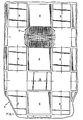
- FIG. 1 is a top plan view in broken section of a portion of a module substrate illustrating the placement of integrated circuit devices, EC devices, and EC lines.
- FIG. 2 is a schematic view in perspective that illustrates buried EC lines in the substrate and their relationship to deletable EC pads and integrated circuit devices.
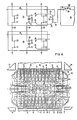
- FIGS. 3 and 4 are detailed views of structures for interconnecting X and Y lines on EC devices.
- FIG. 5 is a schematic view of a portion of X-Y lines on an EC device illustrating their relationship to the EC pads and deletable links for tailoring the EC device.
- FIG. 6 is a schematic view of buried EC lines in the substrate between devices, which illustrates an EC line connection between two spaced devices.
- FIG. 7 is a plan view, in enlarged scale, of a surface metallurgy pattern on the substrate, similar to the pattern in FIG. 1.
- FIG. 1 there is illustrated a top view of a module substrate 10 including integrated circuit devices 12, engineering change devices 14 and a typical fan-out pattern 15 terminating in EC pads (FIG. 7).
- the substrate 10 is typically a multilayer ceramic (MLC) substrate of the type described in the above-cited U.S. Patent 4,245,273.
- MLC multilayer ceramic
- Substrate 10 is formed of a plurality of laminated green ceramic sheets that have been punched to form via holes and a conductive metal line pattern formed thereon.
- the conductive lines collectively form an internal metallurgy system that interconnects the devices 12 with each other and to a plurality of I/O terminals on the opposite side, not shown.
- the laminated sheet assembly is subsequently sintered forming a unitary body.
- the substrate is provided with a fan-out pattern 15, also shown in FIG. 7, which can be either formed as a separate surface metallization layer with an overlying dielectric layer, as illustrated in FIG. 1, or in the top surface layers of the substrate (not illustrated).
- the fan-out layer consists basically of conductive lines 13 that connect the solder pads on the surface of substrate 10 joined to the terminals of the device 12 with EC pads 16 on the top surface of the substrate, located in the area between the devices 12. The end of each line 13 terminates in an EC pad 16 and a short deletable line portion 17 wherein the fan-out line can be disconnected from the internal metallization circuity of substrate 10.
- Both the device terminal pads and the EC pads are preferably solder wettable pads which are joined to the terminals of the integrated circuit devices 12 and the terminals of EC devices 14 by solder connections, as described in U.S. Patent 3,429,040.
- both X lines 18 and Y lines 20 surface periodically on the surface of the substrate 10 as pairs of solder pads 26 and 22.
- Deletable links 23 and 24 join the adjacent pads 22 and 26 thus forming continuous metal stripes.
- Pads 22 and 26 are solder wettable. Links 23 and 24 can be either covered with a thin dielectric layer or have a top surface layer that is not solder wettable. This will constrain the solder to the pads 22 and 26 when the solder mass used to make the solder connections is heated to a molten state.
- the buried EC lines are described in the cited U.S. Patent 4,489,364.
- the fan-out pattern 15, as illustrated in FIG. 1, is repeated on each side of devices 12. In general, it is symmetrical about a center line with one-half of the fan-out pattern associated with one device 12, and the other side associated with the adjacent device 12.
- the pads 22 and 26 joined to the buried EC lines are located in the center area as shown.
- the fan-out pattern is preferably a single layer of metallurgy which can be deposited using conventional deposition and etching techniques.
- the pads are formed with a solder-wettable top metal layer, such as copper.
- the link portion can be formed with at least the top layer of a metal that is not solder wettable.
- the link portion can be covered with a thin dielectric layer.
- the stripes of the fan-out layer can be severed with a laser beam to isolate the stripe from the internal metallurgy of the substrate.
- Adjacent sets of pads 22 and 26 can also be electrically isolated by severing portion 23 or 24.
- solder pads to buried EC lines in both the X and Y directions will be accessible in each fan-out pattern 15.
- the lines in the X direction can be made to surface in a short stripe 24 which can be severed.
- Surface lead lines 25 (FIG. 7) joined to the ends of link 24 are joined to pads 26. The use of these pads will become apparent in the following explanation.
- Engineering change (EC) devices 14 are each provided with a solder pad configuration that is the mirror image of the solder pad configuration of fan-out pattern 15.
- Devices 14 have a tailorable metallurgy system 30, 32, 34, 36 that will permit making electrical connections between the various solder pads of the fan-out pattern 15.
- the substrate 10 is tested to determine if any of the internal buried lines are defective, the appropriate lines are severed in pattern 15 on substrate 10, the metallurgy of device is tailored to make the required electrical connections between the various pads to correct the substrate defects, and the device 14 is joined to the substrate using solder joining techniques to join the respective solder pads.
- the same technique can be used to alter the circuit arrangement of the substrate, i.e. make engineering and design changes.
- EC devices 14 are each provided with a solder pad configuration that is the mirror image of the solder pad configuration of fan-out pattern 15.
- Devices 14 have a tailorable metallurgy system that will permit making electrical connections between the various solder pads of fan-out pattern 15.
- FIG. 5 of the drawings there is illustrated a schematic circuit diagram of a representative portion of the circuit of an EC device 14.
- Each pad 16′ is connected to a single stripe 30 that extends in the X direction.
- stripes 30 are all on a single metallurgy level.
- a similar set of stripes 30 and pads 16′ (not shown) can be provided beneath the set of stripes 30 of FIG. 5.
- the row of pads 16′ associated with each set of stripes 30 is related to a similar row of EC pads 16 on substrate 10.
- a plurality of pads 22′ are joined to stripes 32 that extend in the Y direction.
- a set of pads 26′ joined to stripes 34 are located between stripes 32.
- Pads 22′ and 26′ correspond in placement and spacing to pads 22 and 26 on substrate 10.
- the stripes 32 and 34 are preferably formed in the same metallurgy layer which is electrically isolated from stripes 30 by a suitable dielectric layer. Surface pads 22′ and 26′ are solder wettable.
- Connection 36 can be a connection 36A, as illustrated in FIG. 3 or a connection 36B, as illustrated in FIG. 4.
- Connection 36A is a personalized connection that is selectively formed on substrate 14 after it has been determined which connections must be made to form the proper EC changes.
- the printed connection 36A is made to connect vias 38 and 40 by suitable deposition and subtractive etching techniques that are well-known in the art. If the top stripe is not covered by a dielectric layer, the connection is made directly to the exposed stripe, without the need for a via.
- Device 14 is formed without connections 36A, and tailored by adding the needed connections after they have been determined.
- link 36B is formed during the metallization of the device 14.
- Link 36B has a thin portion which can be blown by applying a suitable electrical current across the connection, using pads 16′, 22′ and 26′ as terminals. After it has been determined which connections are needed to make the EC changes, the remaining links are broken. Links 36B can also be broken with a laser pulse.
- the aforedescribed metallurgy lines can be used to interconnect any solder pad 16 to any EC pad 22 or 26 on substrate 10.
- Stripes 39 which extend in the X direction and are preferably in the same metallurgy layer as stripes 30 can be used to join EC pads 22, associated with EC lines in the Y direction, to EC pads 26, associated with EC lines 18 in the X direction in substrate 10. Lines are each joined to a pad 41′ which can be joined to similarly placed solder pads 41 on substrate 10. The primary use, however, of pad 41′ is to provide an electrical connection to blow out the unneeded links 36.
- a pad 26′ can be connected to a pad 22′ by leaving or forming the link connections 36 at the juncture of the associated stripe 34 and stripe 39, and the juncture of stripe 39 and the associated stripe 32.
- the fan-out line 50 (FIG. 7) is electrically isolated from the internal electrical network of substrate 10 by severing the stripe portion 52.
- the metallurgy pattern on device 14 is then tailored to connect the substrate solder pad 50 to 51.
- the method of making a connection in the device metallurgy between an I/O fan-out pad and an engineering change line pad was described previously.
- a similar procedure is used to join the I/O terminal of the integrated circuit device 12 to an engineering change line connection 53 (FIG. 6).
- a connection 44 between pads 22 and 26, under a different EC device pad 14 located at the intersection of the chosen X and Y EC lines 18 and 20 respectively must be established in EC device 14 overlying the intersecting lines.
- the procedure for tailoring the metallurgy system of device 14 to interconnect EC pads from an X and Y EC lines, i.e. pads 22′ and 26′ was described previously.
- the delete stripes 52 and 54 are severed to isolate a segment of EC line 18.
- Delete stripes 56 and 58 are severed to electrically isolate a segment of EC line 20.
- the devices are joined to the solder pads associated with the respective pads of the fan-out patterns 15. This establishes an engineering change, connecting lead points 53 to 55 which are each connected in turn to selected I/O terminals under different separated integrated circuit devices 12 as previously described in connecting solder pads 16 to 22.
- a row of solder pads 41 can be provided along the edge of fan-out pattern 15 on substrate 10. Lines, either on the surface or buried, join these pads to similar placed pads under the adjacent EC devices which pads are connected to EC lines that extend in the X direction. Pads 41′ (FIG. 5) are connected to pads 41 (FIG. 7) of device 10. Thus, a link connection 36 can be made on EC device metallurgy to join solder pads 22, which are connected to the EC lines that extend in the Y direction to solder pads 26 in the adjacent pattern that are joined to EC lines 18 in the X direction.
Claims (10)
- Module pour un ensemble de dispositifs semi-conducteurs à circuits intégrés, comprenant
un substrat (10) de matériau isolant ayant une surface supérieure et des jeux de plots à braser de dispositif, situés sur cette surface et destinés à être reliés à des plots de dispositifs semi-conducteurs (12) à circuits intégrés, une circuiterie de métallisation interne située à l'intérieur du substrat (10) et destinée à interconnecter électriquement ces dispositifs (12) à circuits intégrés montés sur ladite surface, des plots à braser (16) de modification technique, situés sur ladite surface à proximité des dispositifs (12) et ayant des connexions supprimables à la circuiterie de métallisation interne, des lignes (13) de métallisation de distribution se trouvant sur le substrat (10) et reliant les plots à braser de dispositif à des plots à braser (16) de modification technique respectifs, des lignes de modification technique (18, 20) noyées dans le substrat (10) et comportant une pluralité de moyens de rupture mutuellement espacés par des intervalles réguliers, des trous d'interconnexion entre couches, s'étendant à ladite surface depuis les extrémités des moyens de rupture et se terminant par des plots à braser (22, 26) de lignes de modification technique au-dessus des trous d'interconnexion, ainsi qu'une ligne (23, 24) supprimable reliant chaque paire desdits plots à braser (22, 26) de lignes de modification technique, caractérisé par:
des dispositifs (14) de modification technique comportant des plots à braser (16', 22', 26') agencés pour correspondre aux plots à braser (16) de modification technique et aux plots à braser (22, 26) de lignes de modification technique sur le substrat (10), ainsi qu'un système de métallisation (30, 32, 34, 36) adaptable aux besoins sur chaque dispositif (14) de modification technique, système qui est conçu pour raccorder sélectivement les plots à braser (16', 22', 26') sur ce dispositif,
le dispositif (14) de modification technique étant conçu pour, lorsqu'il attaché au substrat (10), raccorder sélectivement des plots à braser (16) de modification technique à des plots à braser (22, 26) coordonnés adjacents de lignes de modification technique, de manière à modifier ainsi la circuiterie de métallisation interne du substrat (10). - Module selon la revendication 1, dans lequel le substrat (10) est un substrat céramique multicouche et dans lequel les plots à braser (16) de modification technique sont connectés à la circuiterie de métallisation interne par une partie de ligne (17) de métallisation supprimable sur ladite surface.
- Module selon la revendication 1 ou 2, dans lequel les lignes (13) de métallisation de distribution sont situées dans une seule couche sur ladite surface du substrat (10) et sont couvertes par une couche de matériau diélectrique.
- Module selon une des revendications précédentes, dans lequel les lignes noyées de modification technique sont constituées d'une première série de lignes parallèles (18) s'étendant suivant la direction X et d'une deuxième série de lignes parallèles (20) s'étendant suivant la direction X.
- Module selon une des revendications précédentes, dans lequel les plots à braser (16) de modification technique et les plots à braser (22, 26) des lignes de modification techniques sont situés entre les plots à braser de dispositif pour les dispositifs (12) voisins.
- Module selon une des revendications précédentes, dans lequel toutes les connexions électriques entre les dispositifs (12) à circuits intégrés et les plots à braser de dispositif sont des connexions brasées à refusion et toutes les connexions électriques entre les plots à braser (16', 22', 26') sur les dispositifs (14) de modification technique, les plots à braser (16) de modification technique et les plots à braser (22, 26) des lignes de modification technique, sont des connexions brasées à refusion.
- Module selon une des revendications précédentes, dans lequel le système de métallisation adaptable aux besoins sur le dispositif (14) de modification technique est constitué d'une pluralité de bandes conductrices (30, 39) parallèles s'étendant suivant la direction X, une pluralité de bandes conductrices (32, 34) parallèles s'étendant suivant la direction Y, une couche de matériau diélectrique séparant les pluralités de lignes conductrices X et Y, une connexion électrique supprimable (36) adjacente à chacune des intersections des bandes conductrices Y et X, connexion qui relie électriquement les bandes respectives, les plots à braser (16', 22', 26', 41') étant reliés à des bandes respectives de chacune desdites bandes s'étendant suivant les directions X et Y.
- Module selon la revendication 7, dans lequel les connexions électriques supprimables sont constituées chacune d'une mince ligne conductrice fusible (36B).
- Procédé pour modifier l'interconnexion électrique d'une pluralité de dispositifs (12) à circuits intégrés montés sur une surface supérieure du substrat (10) d'un module et interconnectés électriquement par une circuiterie de métallisation interne, se trouvant à l'intérieur du substrat (10), comprenant:
former sur ladite surface, à proximité des dispositifs (12), des plots à braser (16) de modification technique, qui sont connectés électriquement par des lignes (13) de métallisation de distribution à des bornes des dispositifs (12) à circuits intégrés et sont connectés à la circuiterie de métallisation interne d'une manière permettant de supprimer la connexion,
former des lignes de modification technique (18, 20) noyées dans le substrat (10) et
former des moyens de rupture mutuellement espacés par des intervalles réguliers dans les lignes de modification technique (18, 20) et des trous d'interconnexion aux extrémités de ces moyens de rupture, trous qui s'étendent jusqu'à ladite surface du substrat (10), de même que des plots à braser (22, 26) de lignes de modification technique au-dessus chaque trou d'interconnexion et des lignes de surface supprimables (23, 24) qui relient chaque paire de plots à braser (22, 26) adjacents d'une ligne de modification technique, caractérisé par
la formation de dispositifs (14) de modification technique avec une série de plots à braser (16', 22', 26') disposés suivant un motif correspondant aux plots à braser (16) de modification technique et aux plots à braser (22, 26) des lignes de modification technique, ainsi qu'avec un système de métallisation (30, 32, 34, 36) adaptable aux besoins pour connecter électriquement, de façon sélective, les plots à braser (16', 22', 26') sur le dispositif (14) de modification technique,
l'adaptation aux besoins du système de métallisation (30, 32, 34, 36) du dispositif (14) de modification technique afin de réaliser la modification désirée dans la circuiterie de métallisation interne du substrat (10) et
le raccordement des plots à braser (16', 22', 26') sur le dispositif (14) de modification technique aux plots à braser (16) de modification technique et aux plots à braser (22, 26) des lignes de modification technique sur le substrat (10) par des techniques de refusion de brasure.
- Procédé selon la revendication 9, dans lequel le dispositif (14) de modification technique est pourvu de bandes métalliques de liaison fusibles (36B) qui connectent électriquement tous les plots à braser (16', 22', 26'), le procédé comprenant l'étape consistant à
supprimer sélectivement des bandes métalliques de liaison fusibles (36B) par l'application sélective de courants électriques, en laissant subsister les connexions nécessaires pour produire seulement les modifications désirées dans la circuiterie de métallisation interne du substrat (10).
Applications Claiming Priority (2)
| Application Number | Priority Date | Filing Date | Title |
|---|---|---|---|
| US792708 | 1985-10-28 | ||
| US06/792,708 US4652974A (en) | 1985-10-28 | 1985-10-28 | Method and structure for effecting engineering changes in a multiple device module package |
Publications (3)
| Publication Number | Publication Date |
|---|---|
| EP0220503A2 EP0220503A2 (fr) | 1987-05-06 |
| EP0220503A3 EP0220503A3 (en) | 1989-05-31 |
| EP0220503B1 true EP0220503B1 (fr) | 1992-05-27 |
Family
ID=25157814
Family Applications (1)
| Application Number | Title | Priority Date | Filing Date |
|---|---|---|---|
| EP86113233A Expired - Lifetime EP0220503B1 (fr) | 1985-10-28 | 1986-09-26 | Procédé et structure pour permettre un changement voulu dans un ensemble de dispositifs modulaires |
Country Status (5)
| Country | Link |
|---|---|
| US (1) | US4652974A (fr) |
| EP (1) | EP0220503B1 (fr) |
| JP (1) | JPS62101062A (fr) |
| CA (1) | CA1236926A (fr) |
| DE (1) | DE3685472D1 (fr) |
Families Citing this family (38)
| Publication number | Priority date | Publication date | Assignee | Title |
|---|---|---|---|---|
| US5165166A (en) * | 1987-09-29 | 1992-11-24 | Microelectronics And Computer Technology Corporation | Method of making a customizable circuitry |
| AU610249B2 (en) * | 1987-09-29 | 1991-05-16 | Microelectronics And Computer Technology Corporation | Customizable circuitry |
| US5039628A (en) * | 1988-02-19 | 1991-08-13 | Microelectronics & Computer Technology Corporation | Flip substrate for chip mount |
| US4926241A (en) * | 1988-02-19 | 1990-05-15 | Microelectronics And Computer Technology Corporation | Flip substrate for chip mount |
| US4888665A (en) * | 1988-02-19 | 1989-12-19 | Microelectronics And Computer Technology Corporation | Customizable circuitry |
| US5081561A (en) * | 1988-02-19 | 1992-01-14 | Microelectronics And Computer Technology Corporation | Customizable circuitry |
| JPH036844U (fr) * | 1989-06-05 | 1991-01-23 | ||
| US5060116A (en) * | 1990-04-20 | 1991-10-22 | Grobman Warren D | Electronics system with direct write engineering change capability |
| US5224022A (en) * | 1990-05-15 | 1993-06-29 | Microelectronics And Computer Technology Corporation | Reroute strategy for high density substrates |
| US5162792A (en) * | 1990-08-03 | 1992-11-10 | American Telephone And Telegraph Company | On-the-fly arrangement for interconnecting leads and connectors |
| US5220490A (en) * | 1990-10-25 | 1993-06-15 | Microelectronics And Computer Technology Corporation | Substrate interconnect allowing personalization using spot surface links |
| US5155577A (en) * | 1991-01-07 | 1992-10-13 | International Business Machines Corporation | Integrated circuit carriers and a method for making engineering changes in said carriers |
| US5184284A (en) * | 1991-09-03 | 1993-02-02 | International Business Machines Corporation | Method and apparatus for implementing engineering changes for integrated circuit module |
| US5243140A (en) * | 1991-10-04 | 1993-09-07 | International Business Machines Corporation | Direct distribution repair and engineering change system |
| US5247735A (en) * | 1991-12-18 | 1993-09-28 | International Business Machines Corporation | Electrical wire deletion |
| DE4222402A1 (de) * | 1992-07-08 | 1994-01-13 | Daimler Benz Ag | Anordnung für die Mehrfachverdrahtung von Mulichipmodulen |
| US5432708A (en) * | 1992-10-08 | 1995-07-11 | Aptix Corporation | Multichip module integrated circuit device having maximum input/output capability |
| US5539186A (en) * | 1992-12-09 | 1996-07-23 | International Business Machines Corporation | Temperature controlled multi-layer module |
| US5497027A (en) * | 1993-11-30 | 1996-03-05 | At&T Global Information Solutions Company | Multi-chip module packaging system |
| US5834824A (en) * | 1994-02-08 | 1998-11-10 | Prolinx Labs Corporation | Use of conductive particles in a nonconductive body as an integrated circuit antifuse |
| US5726482A (en) * | 1994-02-08 | 1998-03-10 | Prolinx Labs Corporation | Device-under-test card for a burn-in board |
| US5917229A (en) * | 1994-02-08 | 1999-06-29 | Prolinx Labs Corporation | Programmable/reprogrammable printed circuit board using fuse and/or antifuse as interconnect |
| US5808351A (en) * | 1994-02-08 | 1998-09-15 | Prolinx Labs Corporation | Programmable/reprogramable structure using fuses and antifuses |
| US5572409A (en) * | 1994-02-08 | 1996-11-05 | Prolinx Labs Corporation | Apparatus including a programmable socket adapter for coupling an electronic component to a component socket on a printed circuit board |
| US5813881A (en) * | 1994-02-08 | 1998-09-29 | Prolinx Labs Corporation | Programmable cable and cable adapter using fuses and antifuses |
| US5537108A (en) * | 1994-02-08 | 1996-07-16 | Prolinx Labs Corporation | Method and structure for programming fuses |
| US6101710A (en) * | 1994-12-14 | 2000-08-15 | International Business Machines Corporation | Method for facilitating engineering changes in a multiple level circuit package |
| US5962815A (en) * | 1995-01-18 | 1999-10-05 | Prolinx Labs Corporation | Antifuse interconnect between two conducting layers of a printed circuit board |
| US5937515A (en) * | 1995-04-25 | 1999-08-17 | Johnson; Morgan T. | Reconfigurable circuit fabrication method |
| US5906042A (en) * | 1995-10-04 | 1999-05-25 | Prolinx Labs Corporation | Method and structure to interconnect traces of two conductive layers in a printed circuit board |
| US5767575A (en) * | 1995-10-17 | 1998-06-16 | Prolinx Labs Corporation | Ball grid array structure and method for packaging an integrated circuit chip |
| US5872338A (en) * | 1996-04-10 | 1999-02-16 | Prolinx Labs Corporation | Multilayer board having insulating isolation rings |
| US6034427A (en) * | 1998-01-28 | 2000-03-07 | Prolinx Labs Corporation | Ball grid array structure and method for packaging an integrated circuit chip |
| FR2810158B1 (fr) * | 2000-06-09 | 2002-08-30 | Centre Nat Etd Spatiales | Procede pour realiser une permutation d'entrees/sorties de plusieurs pistes a branches paralleles d'un circuit integre et circuit obtenu |
| DE10054114A1 (de) | 2000-10-31 | 2002-05-16 | Dupont Performance Coatings | Verfahren zur Herstellung von Pulverlackzusammensetzungen |
| US6954984B2 (en) * | 2002-07-25 | 2005-10-18 | International Business Machines Corporation | Land grid array structure |
| US6700196B1 (en) * | 2002-09-23 | 2004-03-02 | Honeywell Federal Manufacturing & Technologies | Programmable multi-chip module |
| US7299102B2 (en) * | 2004-12-02 | 2007-11-20 | Norman Ken Ouchi | Method and system for engineering change implementation |
Family Cites Families (6)
| Publication number | Priority date | Publication date | Assignee | Title |
|---|---|---|---|---|
| US3378920A (en) * | 1966-01-26 | 1968-04-23 | Air Force Usa | Method for producing an interconnection matrix |
| US4089734A (en) * | 1974-09-16 | 1978-05-16 | Raytheon Company | Integrated circuit fusing technique |
| FR2404990A1 (fr) * | 1977-10-03 | 1979-04-27 | Cii Honeywell Bull | Substrat d'interconnexion de composants electroniques a circuits integres, muni d'un dispositif de reparation |
| US4254445A (en) * | 1979-05-07 | 1981-03-03 | International Business Machines Corporation | Discretionary fly wire chip interconnection |
| US4245273A (en) * | 1979-06-29 | 1981-01-13 | International Business Machines Corporation | Package for mounting and interconnecting a plurality of large scale integrated semiconductor devices |
| US4489364A (en) * | 1981-12-31 | 1984-12-18 | International Business Machines Corporation | Chip carrier with embedded engineering change lines with severable periodically spaced bridging connectors on the chip supporting surface |
-
1985
- 1985-10-28 US US06/792,708 patent/US4652974A/en not_active Expired - Fee Related
-
1986
- 1986-05-22 CA CA000509769A patent/CA1236926A/fr not_active Expired
- 1986-08-20 JP JP61193029A patent/JPS62101062A/ja active Granted
- 1986-09-26 DE DE8686113233T patent/DE3685472D1/de not_active Expired - Fee Related
- 1986-09-26 EP EP86113233A patent/EP0220503B1/fr not_active Expired - Lifetime
Non-Patent Citations (1)
| Title |
|---|
| IBM TECHNICAL DISCLOSURE BULLETIN, vol. 24, no. 11 A, April 1982: pages 5554-5556, New York, US; E. HUBACHER et al.: "Shared EC PAD design" * |
Also Published As
| Publication number | Publication date |
|---|---|
| EP0220503A3 (en) | 1989-05-31 |
| DE3685472D1 (de) | 1992-07-02 |
| US4652974A (en) | 1987-03-24 |
| JPH0226393B2 (fr) | 1990-06-08 |
| JPS62101062A (ja) | 1987-05-11 |
| CA1236926A (fr) | 1988-05-17 |
| EP0220503A2 (fr) | 1987-05-06 |
Similar Documents
| Publication | Publication Date | Title |
|---|---|---|
| EP0220503B1 (fr) | Procédé et structure pour permettre un changement voulu dans un ensemble de dispositifs modulaires | |
| US4489364A (en) | Chip carrier with embedded engineering change lines with severable periodically spaced bridging connectors on the chip supporting surface | |
| AU610249B2 (en) | Customizable circuitry | |
| EP0083405B1 (fr) | Support de puce pour circuits intégrés à grande échelle et un procédé pour la fabrication du support | |
| EP0098932B1 (fr) | Système à multi-niveaux réparable pour dispositif semi-conducteur | |
| US5165166A (en) | Method of making a customizable circuitry | |
| US4888665A (en) | Customizable circuitry | |
| EP0530185B1 (fr) | Systeme electronique ayant une capacite de changements techniques par application directe de depots metalliques | |
| US4991000A (en) | Vertically interconnected integrated circuit chip system | |
| EP0073149B1 (fr) | Module de montage pour puce semi-conductrice | |
| US5488542A (en) | MCM manufactured by using thin film multilevel interconnection technique | |
| EP0226433B1 (fr) | Circuit imprimé à haute densité | |
| US5354955A (en) | Direct jump engineering change system | |
| EP0018489A2 (fr) | Module pour matrice de pastilles à circuits integrés comprenant des fils adaptables pour l'interconnection | |
| JPH06302759A (ja) | 集積回路キャリアおよびその回路構成変更方法 | |
| EP0166401B1 (fr) | Circuit électrique à module | |
| US5081561A (en) | Customizable circuitry | |
| EP0268111A2 (fr) | Procédé pour effectuer une modification technique des interconnexions entre plusieurs circuits intégrés en utilisant des pièces intermédiaires | |
| JPH01241140A (ja) | テープ・ボンデイング・パツケージ | |
| JPH03215995A (ja) | 多層配線モジュール | |
| US7514798B2 (en) | Arrangement for the protection of three-dimensional structures on wafers | |
| KR20000005426A (ko) | 반도체 장치, 반도체 장치 제조 프로세스, 다이 입출력 패턴 재구성 방법 및 다이 적응성 반도체 장치어셈블리 설계 방법 | |
| JPH1098131A (ja) | 拡散パターニング技術を用いたファインピッチ・バイア形成 | |
| JPS58137294A (ja) | 電気的相互接続パツケ−ジの製造方法 | |
| JP2000138251A (ja) | 半導体装置及び配線基板 |
Legal Events
| Date | Code | Title | Description |
|---|---|---|---|
| PUAI | Public reference made under article 153(3) epc to a published international application that has entered the european phase |
Free format text: ORIGINAL CODE: 0009012 |
|
| AK | Designated contracting states |
Kind code of ref document: A2 Designated state(s): DE FR GB IT |
|
| 17P | Request for examination filed |
Effective date: 19870821 |
|
| PUAL | Search report despatched |
Free format text: ORIGINAL CODE: 0009013 |
|
| AK | Designated contracting states |
Kind code of ref document: A3 Designated state(s): DE FR GB IT |
|
| 17Q | First examination report despatched |
Effective date: 19910211 |
|
| GRAA | (expected) grant |
Free format text: ORIGINAL CODE: 0009210 |
|
| AK | Designated contracting states |
Kind code of ref document: B1 Designated state(s): DE FR GB IT |
|
| PG25 | Lapsed in a contracting state [announced via postgrant information from national office to epo] |
Ref country code: IT Free format text: LAPSE BECAUSE OF FAILURE TO SUBMIT A TRANSLATION OF THE DESCRIPTION OR TO PAY THE FEE WITHIN THE PRE;WARNING: LAPSES OF ITALIAN PATENTS WITH EFFECTIVE DATE BEFORE 2007 MAY HAVE OCCURRED AT ANY TIME BEFORE 2007. THE CORRECT EFFECTIVE DATE MAY BE DIFFERENT FROM THE ONE RECORDED.SCRIBED TIME-LIMIT Effective date: 19920527 |
|
| REF | Corresponds to: |
Ref document number: 3685472 Country of ref document: DE Date of ref document: 19920702 |
|
| ET | Fr: translation filed | ||
| PLBE | No opposition filed within time limit |
Free format text: ORIGINAL CODE: 0009261 |
|
| STAA | Information on the status of an ep patent application or granted ep patent |
Free format text: STATUS: NO OPPOSITION FILED WITHIN TIME LIMIT |
|
| 26N | No opposition filed | ||
| PGFP | Annual fee paid to national office [announced via postgrant information from national office to epo] |
Ref country code: DE Payment date: 19950921 Year of fee payment: 10 |
|
| PGFP | Annual fee paid to national office [announced via postgrant information from national office to epo] |
Ref country code: GB Payment date: 19960827 Year of fee payment: 11 |
|
| PGFP | Annual fee paid to national office [announced via postgrant information from national office to epo] |
Ref country code: FR Payment date: 19960909 Year of fee payment: 11 |
|
| PG25 | Lapsed in a contracting state [announced via postgrant information from national office to epo] |
Ref country code: DE Effective date: 19970603 |
|
| PG25 | Lapsed in a contracting state [announced via postgrant information from national office to epo] |
Ref country code: GB Free format text: LAPSE BECAUSE OF NON-PAYMENT OF DUE FEES Effective date: 19970926 |
|
| PG25 | Lapsed in a contracting state [announced via postgrant information from national office to epo] |
Ref country code: FR Free format text: THE PATENT HAS BEEN ANNULLED BY A DECISION OF A NATIONAL AUTHORITY Effective date: 19970930 |
|
| GBPC | Gb: european patent ceased through non-payment of renewal fee |
Effective date: 19970926 |
|
| REG | Reference to a national code |
Ref country code: FR Ref legal event code: ST |