EP0213562A2 - Circuit de traitement de signaux comportant un transistor à effet de champ MOSFET et des transistors bipolaires - Google Patents
Circuit de traitement de signaux comportant un transistor à effet de champ MOSFET et des transistors bipolaires Download PDFInfo
- Publication number
- EP0213562A2 EP0213562A2 EP86111595A EP86111595A EP0213562A2 EP 0213562 A2 EP0213562 A2 EP 0213562A2 EP 86111595 A EP86111595 A EP 86111595A EP 86111595 A EP86111595 A EP 86111595A EP 0213562 A2 EP0213562 A2 EP 0213562A2
- Authority
- EP
- European Patent Office
- Prior art keywords
- signal
- transistor
- mosfet
- npn
- base
- Prior art date
- Legal status (The legal status is an assumption and is not a legal conclusion. Google has not performed a legal analysis and makes no representation as to the accuracy of the status listed.)
- Granted
Links
Images


Classifications
-
- H—ELECTRICITY
- H03—ELECTRONIC CIRCUITRY
- H03D—DEMODULATION OR TRANSFERENCE OF MODULATION FROM ONE CARRIER TO ANOTHER
- H03D7/00—Transference of modulation from one carrier to another, e.g. frequency-changing
- H03D7/12—Transference of modulation from one carrier to another, e.g. frequency-changing by means of semiconductor devices having more than two electrodes
-
- H—ELECTRICITY
- H03—ELECTRONIC CIRCUITRY
- H03G—CONTROL OF AMPLIFICATION
- H03G1/00—Details of arrangements for controlling amplification
- H03G1/0005—Circuits characterised by the type of controlling devices operated by a controlling current or voltage signal
- H03G1/0035—Circuits characterised by the type of controlling devices operated by a controlling current or voltage signal using continuously variable impedance elements
- H03G1/0082—Circuits characterised by the type of controlling devices operated by a controlling current or voltage signal using continuously variable impedance elements using bipolar transistor-type devices
Definitions
- the present invention relates to a signal-processing circuit having a field-effect transistor and a bipolar transistor connected in cascade to the field-effect transistor.
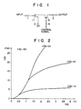
- a gain-controlled amplifier for use in a high-frequency amplifying stage, such as a tuner, has the structure shown in Fig. l or that shown in Fig. 4.
- the amplifier of Fig. l is disclosed in Japanese Patent Disclosure Sho 6l-l60l70.
- This circuit comprises a MOSFET ll (metal oxide semiconductor field-effect transistor) used as the first stage, and another MOSFET l2 used as the second stage and cascade-connected to MOSFET ll.
- the gate of FET ll is connected to input terminal l which in turn is coupled to an input tuning circuit (not shown), and can receive a DC bias signal and an input signal from the tuning circuit via input terminal l.
- a predetermined voltage (usually, the ground potential) is applied to the gate of FET l2 through gain control terminal 3.
- the drain of FET l2 is connected to output terminal 4.
- the amplifier shown in Fig. 4 is disclosed in Integrated Electronics , McGraw-Hill, Inc., pp 566-569.
- This circuit comprises an NPN transistor l3 used as the first stage, and an NPN transistor l4 used as the second state and which is cascade-connected to NPN transistor l3.
- the base of transistor l3 is coupled to input terminal l.
- the emitter of transistor l4 is connected to terminal 2 held at a predetermined potential.
- the base and collector of transistor l4 are connected to gain control terminal 3 and output terminal 4, respectively.
- the amplifier of Fig. l amplifies the signal supplied to input terminal l when a predetermined operation current flows through first-stage FET ll and second-stage FET l2.
- the amplifier has one drawback, however. Its input-output characteristic contains prominent third distortion components. This is because the MOSFETs have a high equivalent resistance, due to their structure and function. More specifically, the amplifier exhibits the DC input-output characteristics shown in Fig. 2, when a gain control voltage is applied to the gate of FET l2.
- the DC input-output characteristic is the relation between voltage Vl2 between terminals l and 2, and current I42 flowing between terminals 2 and 4.
- voltage V32 between terminals 2 and 3 (i.e., the gain-controlling voltage) is regarded as a parameter, and voltage V42 between terminals 2 and 4 is fixed at 6V.
- the equivalent resistance of FETs ll and l2 affects the prominence of the third distortion components of output current I42 near the boundary between the region where the characteristic of FET ll is predominant and current I42 is thus small, and the region where the characteristic of FET l2 is predominant and current I42 is large.
- the inflection points shown in Fig. 3 correspond to the third distortion components of the input-output characteristic curve (Fig. 2). As Fig. 3 clearly shows, there are inflection points where the slope of the characteristic curve is steep. This means that the characteristic curve has prominent third distortion components. Fig. 3 further reveals that there are two inflection points where gain-controlling voltage V32 falls. If such is the case, the third distortion components will become more prominent.
- the equivalent resistance of the collector-emitter path of transistor l3 is far lower than that of either MOSFET used in the amplifier of Fig. l.
- the input-output characteristic curve of the amplifier shown in Fig. 4 also has prominent third distortion components. This is inevitably because the first-stage transistor is a bipolar transistor.
- the object of this invention is to provide a signal-processing circuit whose input-output characteristic curve has small distortion components; in particular, small third distortion components.
- a signal-processing circuit comprises means for receiving a first signal; a metal oxide semiconductor field-effect (MOSFET) whose gate is connected to the means for receiving the first signal and whose current path is supplied with a predetermined potential; means for receiving a second signal; means for supplying an output signal; and an NPN bipolar transistor whose collector-emitter path is connected at one end to the current path of the MOSFET and at the other end to the means for supplying the output signal, whose base is connected to the means for receiving the second signal, and whose base current is controlled by the second signal supplied from the means for receiving the second signal.
- the first signal can therefore be controlled by the second signal.
- the signal-processing circuit can have an input-output characteristic curve with negligible distortion components, particularly negligible third distortion components.
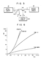
- Fig. 5 is a circuit diagram of a gain-controlled amplifier according to one embodiment of the invention.
- the source of N-channel enhancement or depletion enhancement MOSFET 2l is connected to terminal 2 to which a predetermined potential (usually, the ground potential) is applied.
- the gate of FET 2l is coupled to input terminal l which in turn is connected to input tuning circuit 23.
- the emitter of NPN bipolar transistor 22 is connected to the drain of FET 2l.
- the base of NPN transistor 22 is coupled to gain control terminal 3 which in turn is connected to gain control circuit 24.
- the collector of NPN transistor 22 is connected to output terminal 4 coupled to output tuning circuit 25.
- Input tuning circuit 23 receives a high-frequency signal obtained from, for example, VHF-band TV waves. Circuit 23 supplies this high-frequency signal and, if necessary, a DC bias signal to input terminal l. As a result, a predetermined operation current flows from the power source of output tuning circuit25 to terminal 2 through terminal 4, the collector-emitter path of NPN transistor 22 and the current path of FET 2l. As this current flows through both transistors 2l and 22, the input signal, i.e., the high-frequency signal, is amplified with the gain corresponding to the gain-controlling voltage applied to the base of transistor 22.
- Input voltage Vl2 i.e., the voltage between terminals l and 2) and output current I42 (i.e., the current between terminals 4 and 2) have the relationship illustrated in Fig. 6.
- operation voltage V42 i.e., the voltage between terminals 4 and 2) is set at 6V
- control voltage V32 i.e., the voltage between terminals 3 and 2 is sued as a parameter.
- the first distortion components and second distortion components of the characteristic curve are also less prominent than those of the characteristic curve of the conventional amplifier (Fig. l).
- the gain changes in accordance with control voltage Vl2, same as the conventional gain-controlled amplifiers shown in Figs. l and 4.
- the gain-controlled amplifier of this embodiment can therefore generate an output signal containing distortion components which are less prominent than those of the output signal produced by the conventional gain-controlled amplifiers.
- Fig. 8 The modification of Fig. 8 is characterized in two respects. First, resistor 3l for adjusting the base current of second-stage transistor 22 and protecting the base of transistor 22, is connected between the base of transistor 22 and gain control terminal 3. Secondly, capacitor 32 for grounding high-frequency components of a signal, is connected between the base of transistor 22 and gain control terminal 3. Forward transmission admittance
- Fig. 9 The modification shown in Fig. 9 is also characterized in two respects.
- Darlington-connected NPN transistors 4l and 42 are used in place of second-stage transistor 22.
- capacitor 43 for grounding the high-frequency components of a signal is connected between the base of transistor 4l and gain control terminal 3.
- Capacitor 43 can be coupled between the source of FET 2l and the base of transistor 4l.
- Fig. l0 has three characterizing features.
- Darlington-connected NPN transistors 5l and 52 are used in place of second-stage transistor 22.
- resistor 53 for adjusting the base current of transistor 52 is coupled between the base of transistor 52 and gain control terminal 3.
- capacitor 54 for grounding the high-frequency components of a signal is connected between the base of transistor 5l and gain control terminal 3.
- FET 6l should have similar high-frequency characteristic and are highly sensitive (that is, having a high mutual conductance), same as FET 2l.
- the gate voltage of FET 6l is controlled, thereby controlling the drain current of FET 6l.
- the base current of transistor 22 is controlled.
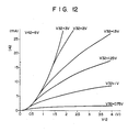
- the amplifier has the input-output characteristic shown in Fig. l2. Its forward transmission admittance
- the amplifier can be gain-controlled and can generate an output signal containing less distortion components than the output signal of the amplifier shown in Fig. 5.
- Fig. l4 shows a modification of the second embodiment (Fig. ll). This modification differs from the amplifier of Fig. ll in three respects.
- Darlington-connected NPN transistors 7l and 72 are used in place of second-stage bipolar transistor 22.
- the current path of control FET 73 is connected between the collector and base of transistor 72.
- capacitor 74 for grounding the high-frequency components of a signal is coupled between the base of transistor 7l and gain control terminal 3. If control FET 73 has excellent DC characteristics, the modification of Fig. l4 can have as good an input-output characteristic as the first and second embodiments shown in Figs. 5 and ll.
- a high-frequency input signal is supplied to terminal l (in other words, the gate of transistor 2l), and a gain control voltage is applied to terminal 3, thereby amplifying the high-frequency input signal by the gain corresponding to the gain control voltage.
- the present invention is not limited to these embodiments.
- Other input signals such as a low-frequency signal or an intermediate-frequency signal, can be amplified.
- Furthermore, first and second signals can be input to terminals l and 3, whereby they are mixed.
- circuits of the above embodiments can be manufactured either in the form of an integrated circuit made by a bipolar/MOS process, or in the form of an assembly of independently made elements.
- the circuits can be manufactured using compound semiconductor, for example GaAs.
- the amplifier shown in Fig. l5 which is a modification of the amplifier shown in Fig. 9, be formed on one pellet mode of silicon, by a bipolar/MOS process, in the form of an integrated circuit is described.
- the amplifier of Fig. l5 is different from that of Fig. 9 in two respects.
- capacitor 43 is connected at one end to the source of FET 2l.
- a bidirectional diode consisting of protective diodes 44 and 45 connected in series and arranged in opposite directions, is connected between the gate and source of FET 2l, thus protecting the gate of FET 2l.
- Fig. l6 is a cross-sectional view of the amplifier of Fig. l5, formed in or on a p-type silicon substrate.
- Fig. l7 is a cross-sectional view of the same amplifier formed on an n-type silicon substrate.
- p-type epitaxial layer ll0B is formed on p-type silicon substrate ll0A.
- Buried layer ll3 having a high n-type impurity concentration (n+-type) is formed at the interface between silicon substrate ll0A and epitaxial layer ll0B.
- Two regions, n-type well region ll4 and n+-type region ll5, are formed in that portion of epitaxial layer ll0B which is located on n+type buried layer ll3.
- Region ll5 is shaped like a ring and surrounds well region ll4, for example.
- p-type regions ll6 and ll7 are formed, set apart from each other.
- n-type region ll8 is formed in the surface region of p-type region ll6, and another n-type region ll9 is formed in the surface region of p-type region ll7.
- Oxide film l20A is formed on epitaxial layer ll0B. Five contact holes are cut in those portions of oxide film l20A which are provided on n+-type region ll5, p-type regions ll6 and ll7, and n-type regions ll8 and ll9.
- Electrodes l2l, l22, l23, and l24 made of aluminum are formed on oxide film l20A. Electrode l2l contacts n+-type region ll5. Electrode l22 contacts p-type region ll7. Electrode l23 connects p-type region l6 and n-type region ll9.
- Electrode l24 connects n-type region ll8 to n-type region l25 corresponding to drain D of MOSFET 2l
- n-type well region ll4, p-type region ll6, and n-type region ll8 correspond to the collector, base, and emitter of first-stage transistor 2l (Fig. l5), respectively
- n-type well region ll4, p-type region ll7, and n-type region ll9 correspond to the collector, base, and emitter of second-stage transistor 42 (Fig. l5), respectively.
- Electrodes l2l and l22 correspond, respectively, to output terminal 4 and gain control terminal 3, both shown in Fig. l5.
- n-type regions l25, l26, and l27, and p+-type region l28 are formed in a surface region of epitaxial layer ll0B.
- p+-type region l29 is formed in the surface region of n-type region l27.
- Insulation film l20B i.e., gate oxide film is formed on that portion of epitaxial layer ll0B which is located between n-type regions l25 and l26.
- Gate electrode l3l is formed on insulation film l20B.
- Thin oxide film l20C is formed on one portion of p+-type region l28.
- Aluminum electrode l32 is formed on thin oxide film l20C.
- Six contact holes are cut in those portions of oxide film l20A formed on epitaxial layer ll0B, which are located in n-type regions l25 and l26, p+-type regions l28, l29, and l30, and gate electrode l3l.
- Electrodes l33, l34, l35, l36, and l37 made of aluminum, are formed on oxide film l20A.
- Electrode l33 contacts n-type region l26.
- Electrodes l34, l35, and l36 contact p+-type regions l28, l29, and l30, respectively.
- Electrode l37 contacts gate electrode l3l.
- N-type regions l25 and l26, and gate electrode l3l correspond to the drain, source, and gate of FET 2l (Fig. l5), respectively.
- Electrodes l37 and l33 correspond to input terminal l and terminal 2 (both shown in Fig. l5), respectively.
- Electrodes l32 and l34 correspond to the electrodes of capacitor 43 (Fig. l5).
- Electrodes l32 and l34 are connected by aluminum wires (not shown) to electrodes l23 and l33, respectively.
- Electrodes l35 and l36 correspond, respectively, to the anodes of diodes 44 and 45, and are connected to electrodes l37 and l33 by wired (not shown).
- the circuit shown in Fig. l5 is made in the form of a pellet, and is attached to a lead frame (not shown) by gold-silicon eutectic or by a resin.
- the lead terminals corresponding to terminals l, 3, and 4, and electrodes l37, l22, and l2l corresponding to input terminal l, gain control terminal 3, and output terminal 4, are connected by a wire-bonding.
- Electrode l33 which is connected to the source of MOSFET 2l and corresponds to terminal 2, is connected to the lead frame by a wire-bonding.
- an oxide film is formed on one major surface of p-type silicon substrate ll0A doped with boron in a concentration of, for example, 4 ⁇ l014 cm ⁇ 3
- the oxide film is patterned, exposing that portion of substrate ll0A in which buried layer ll3 will be formed.
- Antimony in a concentration of 5 ⁇ l019 cm ⁇ 3 is diffused into substrate ll0A, using the patterned oxide film as the diffusion mask, thereby forming n+-type buried layer ll3.
- Epitaxial layer ll0B of silicon containing boron in a concentration l.8 ⁇ l015 cm ⁇ 3 is formed on substrate ll0A; this epitaxial layer has a thickness of 7 to 8 ⁇ m.
- An oxide film is then formed on epitaxial layer ll0B.
- This oxide film is patterned, exposing those portions of epitaxial layer ll0B in which regions ll4, ll5, and l27 will be formed.
- phosphorus is ion-implanted into epitaxial layer ll0B, under acceleration voltage of l50 kev, in a dosage of l ⁇ l015 cm ⁇ 2, thereby forming regions ll4 and l27, and under acceleration voltage of 50 kev, in a dosage of 9 ⁇ l015 cm ⁇ 2, thereby forming region ll5.
- PSG is deposited in the openings of the oxide film.
- the resultant structure is annealed for l5 hours at l200°C in a nitrogen gas atmosphere.
- n-type well region ll4, n+-type region ll5, and n-type region l27 are completed.
- Another oxide film is formed on the surface of the unfinished product, and has a thickness of l80 nm. This oxide film is patterned, to form regions ll6, ll7, l28, l29, and l30.
- boron is ion-implanted into epitaxial layer ll0B under acceleration voltage of 50 kev, in a dosage of l ⁇ l014 cm ⁇ 2, and the resultant structure is annealed for 30 minutes at l000°C in a nitrogen atmosphere, thus forming p-type regions ll6 and ll7.
- boron is ion-implanted into epitaxial layer ll0B under acceleration voltage of 50 kev, in a dosage of l ⁇ l014 cm ⁇ 2, and the unfinished product is annealed for 30 minutes at l000°C in a nitrogen gas atmosphere, thereby forming p+-type regions l28, l29, and l30.
- gate oxide film l20B and oxide film l20C for forming a capacitor are formed.
- Gate electrode l3l having a width of 1.5 ⁇ m is formed of molybdenum silicide (MoSi).
- MoSi molybdenum silicide
- arsenic is ion-implanted into epitaxial layer ll0B under acceleration voltage of 35 kev, in a dosage of l ⁇ l015 cm ⁇ 2, and the resultant structure is annealed for 30 minutes at 900°C in a nitrogen gas atmosphere, thereby forming n-type regions l25 and l26.
- gate electrode l3l arsenic is ion-implanted into regions ll6 and ll7 under acceleration voltage of 35 kev, in a dosage of l ⁇ l015 cm ⁇ 2, and the resultant structure is annealed for 20 minutes at l000°C in a nitrogen gas atmosphere, thereby forming n-type regions ll8 and ll9.
- the oxide film is patterned, thus making contact holes.
- the unfinished product is subjected to thermal oxidation, whereby oxide film l20A is formed.
- An aluminum film is then formed on oxide film l20A.
- the aluminum film is patterned, thereby forming electrodes l2l-l24 and electrodes l32-l37.
- the gain-controlled amplifier shown in Fig. l7 differs from the gain-controlled amplifier of Fig. l6 in the following respects:
- the signal-processing circuit of this invention can be used as a gain controlled amplifiers, since its input-output characteristic curve has far less third distortion components as compared to the characteristic curves of the conventional gain-controlled amplifiers. Hence, it can operate effectively, particularly when it is used as a high-frequency amplifier whose gain is controlled by AGC (automatic gain control) feedback voltage. Further, when the signal-processing circuit is employed as a mixing circuit, it can generate an output signal having negligibly small distortion components; in particularly, negligible third distortion components.
Landscapes
- Engineering & Computer Science (AREA)
- Power Engineering (AREA)
- Amplifiers (AREA)
Applications Claiming Priority (4)
| Application Number | Priority Date | Filing Date | Title |
|---|---|---|---|
| JP189232/85 | 1985-08-28 | ||
| JP18923285 | 1985-08-28 | ||
| JP72950/86 | 1986-03-31 | ||
| JP61072950A JPS62122307A (ja) | 1985-08-28 | 1986-03-31 | 利得制御増幅回路 |
Publications (4)
| Publication Number | Publication Date |
|---|---|
| EP0213562A2 true EP0213562A2 (fr) | 1987-03-11 |
| EP0213562A3 EP0213562A3 (en) | 1989-03-15 |
| EP0213562B1 EP0213562B1 (fr) | 1993-01-13 |
| EP0213562B2 EP0213562B2 (fr) | 1997-11-12 |
Family
ID=26414084
Family Applications (1)
| Application Number | Title | Priority Date | Filing Date |
|---|---|---|---|
| EP86111595A Expired - Lifetime EP0213562B2 (fr) | 1985-08-28 | 1986-08-21 | Circuit de traitement de signaux comportant un transistor à effet de champ MOSFET et des transistors bipolaires |
Country Status (3)
| Country | Link |
|---|---|
| US (1) | US4757276A (fr) |
| EP (1) | EP0213562B2 (fr) |
| DE (1) | DE3687494T3 (fr) |
Cited By (2)
| Publication number | Priority date | Publication date | Assignee | Title |
|---|---|---|---|---|
| EP1020993A1 (fr) * | 1999-01-18 | 2000-07-19 | Alps Electric Co., Ltd. | Circuit d'accord |
| CN103644303A (zh) * | 2013-11-17 | 2014-03-19 | 苏州蓝王机床工具科技有限公司 | 皮带运输机托辊轴端密封圈结构 |
Families Citing this family (11)
| Publication number | Priority date | Publication date | Assignee | Title |
|---|---|---|---|---|
| US5212398A (en) * | 1989-11-30 | 1993-05-18 | Kabushiki Kaisha Toshiba | BiMOS structure having a protective diode |
| US5187110A (en) * | 1990-10-05 | 1993-02-16 | Allied-Signal Inc. | Field effect transistor-bipolar transistor darlington pair |
| US5086282A (en) * | 1990-10-05 | 1992-02-04 | Allied-Signal Inc. | Field effect transistor-bipolar transistor Darlington pair |
| JP3161721B2 (ja) * | 1990-10-19 | 2001-04-25 | 株式会社日立製作所 | 増幅回路及びディスプレイ装置 |
| US5748035A (en) * | 1994-05-27 | 1998-05-05 | Arithmos, Inc. | Channel coupled feedback circuits |
| US5920230A (en) * | 1997-10-21 | 1999-07-06 | Trw Inc. | HEMT-HBT cascode distributed amplifier |
| US6184751B1 (en) * | 1998-08-17 | 2001-02-06 | Motorola, Inc. | Amplifier circuit |
| JP2000278109A (ja) * | 1999-03-19 | 2000-10-06 | Fujitsu Ltd | 高周波スイッチ、切替型高周波スイッチ、および切替型高周波電力増幅器 |
| RU2292997C2 (ru) * | 2003-10-08 | 2007-02-10 | Хитачи Коки Ко. Лтд. | Станок для резки под углом с индикацией угла установки режущего элемента (варианты) |
| JP2006135518A (ja) * | 2004-11-04 | 2006-05-25 | Alps Electric Co Ltd | 高周波増幅器 |
| DE102013206412A1 (de) * | 2013-04-11 | 2014-10-16 | Ifm Electronic Gmbh | Schutzschaltung für eine Signalausgangs-Stufe |
Citations (4)
| Publication number | Priority date | Publication date | Assignee | Title |
|---|---|---|---|---|
| DE1512683A1 (de) * | 1966-02-12 | 1969-08-07 | Emi Ltd | Verstaerker mit steuerbarer Verstaerkung |
| US3882410A (en) * | 1972-12-13 | 1975-05-06 | Song Corp | Gain control circuit |
| GB2002608A (en) * | 1977-08-01 | 1979-02-21 | Pioneer Electronic Corp | Automatic gain control circuit |
| JPS5970006A (ja) * | 1982-10-13 | 1984-04-20 | Hitachi Ltd | ミクサ回路 |
Family Cites Families (3)
| Publication number | Priority date | Publication date | Assignee | Title |
|---|---|---|---|---|
| US3541234A (en) * | 1967-10-20 | 1970-11-17 | Rca Corp | Video circuits employing cascoded combinations of field effect transistors with high voltage,low bandwidth bipolar transistors |
| US3609479A (en) * | 1968-02-29 | 1971-09-28 | Westinghouse Electric Corp | Semiconductor integrated circuit having mis and bipolar transistor elements |
| US4586004A (en) * | 1983-06-27 | 1986-04-29 | Saber Technology Corp. | Logic and amplifier cells |
-
1986
- 1986-08-21 DE DE3687494T patent/DE3687494T3/de not_active Expired - Lifetime
- 1986-08-21 EP EP86111595A patent/EP0213562B2/fr not_active Expired - Lifetime
- 1986-08-25 US US06/899,592 patent/US4757276A/en not_active Expired - Lifetime
Patent Citations (4)
| Publication number | Priority date | Publication date | Assignee | Title |
|---|---|---|---|---|
| DE1512683A1 (de) * | 1966-02-12 | 1969-08-07 | Emi Ltd | Verstaerker mit steuerbarer Verstaerkung |
| US3882410A (en) * | 1972-12-13 | 1975-05-06 | Song Corp | Gain control circuit |
| GB2002608A (en) * | 1977-08-01 | 1979-02-21 | Pioneer Electronic Corp | Automatic gain control circuit |
| JPS5970006A (ja) * | 1982-10-13 | 1984-04-20 | Hitachi Ltd | ミクサ回路 |
Non-Patent Citations (2)
| Title |
|---|
| PATENT ABSTRACTS OF JAPAN, vol. 8, no. 176 (E-260)[1613], 14th August 1984; & JP-A-59 70 006 (HITACHI SEISAKUSHO K.K.) 20-04-1984 * |
| W.HEINLEIN et al.: "ACTIVE FILTERS FOR INTEGRATED CIRCUITS", "Fundamentals and Design Methods", 1974, pages 250-251, Springer-Verlag, New York, US * |
Cited By (2)
| Publication number | Priority date | Publication date | Assignee | Title |
|---|---|---|---|---|
| EP1020993A1 (fr) * | 1999-01-18 | 2000-07-19 | Alps Electric Co., Ltd. | Circuit d'accord |
| CN103644303A (zh) * | 2013-11-17 | 2014-03-19 | 苏州蓝王机床工具科技有限公司 | 皮带运输机托辊轴端密封圈结构 |
Also Published As
| Publication number | Publication date |
|---|---|
| DE3687494T2 (de) | 1993-04-29 |
| DE3687494D1 (de) | 1993-02-25 |
| DE3687494T3 (de) | 1998-06-10 |
| EP0213562B1 (fr) | 1993-01-13 |
| EP0213562B2 (fr) | 1997-11-12 |
| EP0213562A3 (en) | 1989-03-15 |
| US4757276A (en) | 1988-07-12 |
Similar Documents
| Publication | Publication Date | Title |
|---|---|---|
| EP0213562A2 (fr) | Circuit de traitement de signaux comportant un transistor à effet de champ MOSFET et des transistors bipolaires | |
| US5633610A (en) | Monolithic microwave integrated circuit apparatus | |
| US5592124A (en) | Integrated photodiode/transimpedance amplifier | |
| KR100303725B1 (ko) | 상보형금속산화물반도체"또는바이폴라/cmos공정을사용하여n-채널및p-채널접합전계효과트랜지스터및cmos트랜지스터를제조하는방법 | |
| US5498885A (en) | Modulation circuit | |
| JP2000101403A (ja) | 比較増幅検出回路 | |
| Fukuta et al. | GaAs microwave power FET | |
| US6044255A (en) | Radio frequency circuit with integrated elements and method of manufacture | |
| US5614424A (en) | Method for fabricating an accumulated-base bipolar junction transistor | |
| KR900004764B1 (ko) | 신호처리회로 | |
| US4580106A (en) | Differential amplifier with bipolar transistors which is compatible with standard complimentary MOS (CMOS) technology | |
| US4607172A (en) | Bipolar strobed transistor latch for a high gain comparator | |
| US5021859A (en) | High-frequency amplifying semiconductor device | |
| Ogawa et al. | A Long‐Wavelength Optical Receiver Using a Short‐Channel Si‐MOSFET | |
| GB2061655A (en) | Amplifier protection | |
| Aoki et al. | A 1.4-dB-NF variable-gain LNA with continuous control for 2-GHz-band mobile phones using InGaP emitter HBTs | |
| GB1598044A (en) | Hf-amplifier circuit | |
| Kobayashi et al. | A novel monolithic LNA integrating a common-source HEMT with an HBT Darlington amplifier | |
| Erben et al. | Application of a production ready SiGe HBT process to 1.9, 5.7 and 10 GHz low noise MMICs | |
| JP2708442B2 (ja) | 半導体集積回路 | |
| CN115118238B (zh) | 一种基于soi工艺的斩波仪表放大器 | |
| EP0686305A1 (fr) | Procede de fabrication d'un dispositif cmos comportant des elements jfet | |
| US7423485B2 (en) | Differential circuit with improved linearity | |
| JP2878717B2 (ja) | 半導体装置、半導体集積回路装置 | |
| JP3047063B2 (ja) | フォトダイオード |
Legal Events
| Date | Code | Title | Description |
|---|---|---|---|
| PUAI | Public reference made under article 153(3) epc to a published international application that has entered the european phase |
Free format text: ORIGINAL CODE: 0009012 |
|
| 17P | Request for examination filed |
Effective date: 19860918 |
|
| AK | Designated contracting states |
Kind code of ref document: A2 Designated state(s): DE FR GB |
|
| PUAL | Search report despatched |
Free format text: ORIGINAL CODE: 0009013 |
|
| AK | Designated contracting states |
Kind code of ref document: A3 Designated state(s): DE FR GB |
|
| 17Q | First examination report despatched |
Effective date: 19910219 |
|
| GRAA | (expected) grant |
Free format text: ORIGINAL CODE: 0009210 |
|
| AK | Designated contracting states |
Kind code of ref document: B1 Designated state(s): DE FR GB |
|
| REF | Corresponds to: |
Ref document number: 3687494 Country of ref document: DE Date of ref document: 19930225 |
|
| ET | Fr: translation filed | ||
| PLBI | Opposition filed |
Free format text: ORIGINAL CODE: 0009260 |
|
| 26 | Opposition filed |
Opponent name: INTERESSENGEMEINSCHAFT FUER RUNDFUNKSCHUTZRECHTE E Effective date: 19931012 |
|
| PLAB | Opposition data, opponent's data or that of the opponent's representative modified |
Free format text: ORIGINAL CODE: 0009299OPPO |
|
| PLBQ | Unpublished change to opponent data |
Free format text: ORIGINAL CODE: EPIDOS OPPO |
|
| R26 | Opposition filed (corrected) |
Opponent name: INTERESSENGEMEINSCHAFT FUER RUNDFUNKSCHUTZRECHTE E Effective date: 19931012 |
|
| PLAW | Interlocutory decision in opposition |
Free format text: ORIGINAL CODE: EPIDOS IDOP |
|
| PLAW | Interlocutory decision in opposition |
Free format text: ORIGINAL CODE: EPIDOS IDOP |
|
| PUAH | Patent maintained in amended form |
Free format text: ORIGINAL CODE: 0009272 |
|
| STAA | Information on the status of an ep patent application or granted ep patent |
Free format text: STATUS: PATENT MAINTAINED AS AMENDED |
|
| 27A | Patent maintained in amended form |
Effective date: 19971112 |
|
| AK | Designated contracting states |
Kind code of ref document: B2 Designated state(s): DE FR GB |
|
| ET3 | Fr: translation filed ** decision concerning opposition | ||
| REG | Reference to a national code |
Ref country code: GB Ref legal event code: 746 Effective date: 19981026 |
|
| REG | Reference to a national code |
Ref country code: FR Ref legal event code: D6 |
|
| REG | Reference to a national code |
Ref country code: GB Ref legal event code: IF02 |
|
| PGFP | Annual fee paid to national office [announced via postgrant information from national office to epo] |
Ref country code: FR Payment date: 20050809 Year of fee payment: 20 |
|
| PGFP | Annual fee paid to national office [announced via postgrant information from national office to epo] |
Ref country code: GB Payment date: 20050817 Year of fee payment: 20 |
|
| PGFP | Annual fee paid to national office [announced via postgrant information from national office to epo] |
Ref country code: DE Payment date: 20050818 Year of fee payment: 20 |
|
| PG25 | Lapsed in a contracting state [announced via postgrant information from national office to epo] |
Ref country code: GB Free format text: LAPSE BECAUSE OF EXPIRATION OF PROTECTION Effective date: 20060820 |
|
| REG | Reference to a national code |
Ref country code: GB Ref legal event code: PE20 |