EP0206325A2 - Method for fabricating an optical isolator. - Google Patents
Method for fabricating an optical isolator. Download PDFInfo
- Publication number
- EP0206325A2 EP0206325A2 EP86108623A EP86108623A EP0206325A2 EP 0206325 A2 EP0206325 A2 EP 0206325A2 EP 86108623 A EP86108623 A EP 86108623A EP 86108623 A EP86108623 A EP 86108623A EP 0206325 A2 EP0206325 A2 EP 0206325A2
- Authority
- EP
- European Patent Office
- Prior art keywords
- photodiode
- led
- lead
- downset
- optical isolator
- Prior art date
- Legal status (The legal status is an assumption and is not a legal conclusion. Google has not performed a legal analysis and makes no representation as to the accuracy of the status listed.)
- Granted
Links
- 230000003287 optical effect Effects 0.000 title claims abstract description 54
- 238000000034 method Methods 0.000 title claims description 39
- 238000002955 isolation Methods 0.000 claims abstract description 47
- 229920005989 resin Polymers 0.000 claims abstract description 20
- 239000011347 resin Substances 0.000 claims abstract description 20
- 239000000463 material Substances 0.000 claims description 17
- 239000003989 dielectric material Substances 0.000 claims 5
- 238000005538 encapsulation Methods 0.000 claims 2
- 239000012780 transparent material Substances 0.000 claims 1
- 238000004519 manufacturing process Methods 0.000 description 7
- 238000001721 transfer moulding Methods 0.000 description 4
- 230000015556 catabolic process Effects 0.000 description 3
- XEEYBQQBJWHFJM-UHFFFAOYSA-N Iron Chemical compound [Fe] XEEYBQQBJWHFJM-UHFFFAOYSA-N 0.000 description 2
- PXHVJJICTQNCMI-UHFFFAOYSA-N Nickel Chemical compound [Ni] PXHVJJICTQNCMI-UHFFFAOYSA-N 0.000 description 2
- 239000000853 adhesive Substances 0.000 description 2
- 230000001070 adhesive effect Effects 0.000 description 2
- 239000012790 adhesive layer Substances 0.000 description 2
- 150000001875 compounds Chemical class 0.000 description 2
- 230000006835 compression Effects 0.000 description 2
- 238000007906 compression Methods 0.000 description 2
- 230000007423 decrease Effects 0.000 description 2
- 230000000694 effects Effects 0.000 description 2
- 238000000465 moulding Methods 0.000 description 2
- JBRZTFJDHDCESZ-UHFFFAOYSA-N AsGa Chemical compound [As]#[Ga] JBRZTFJDHDCESZ-UHFFFAOYSA-N 0.000 description 1
- 229910001218 Gallium arsenide Inorganic materials 0.000 description 1
- 229910045601 alloy Inorganic materials 0.000 description 1
- 239000000956 alloy Substances 0.000 description 1
- 239000011248 coating agent Substances 0.000 description 1
- 238000000576 coating method Methods 0.000 description 1
- 238000010276 construction Methods 0.000 description 1
- 230000001351 cycling effect Effects 0.000 description 1
- PCHJSUWPFVWCPO-UHFFFAOYSA-N gold Chemical compound [Au] PCHJSUWPFVWCPO-UHFFFAOYSA-N 0.000 description 1
- 229910052737 gold Inorganic materials 0.000 description 1
- 239000010931 gold Substances 0.000 description 1
- 238000003780 insertion Methods 0.000 description 1
- 230000037431 insertion Effects 0.000 description 1
- 229910052742 iron Inorganic materials 0.000 description 1
- 229910052759 nickel Inorganic materials 0.000 description 1
- 239000012811 non-conductive material Substances 0.000 description 1
- 238000004806 packaging method and process Methods 0.000 description 1
- 230000035515 penetration Effects 0.000 description 1
- 229920003223 poly(pyromellitimide-1,4-diphenyl ether) Polymers 0.000 description 1
- 239000011253 protective coating Substances 0.000 description 1
- 239000004065 semiconductor Substances 0.000 description 1
- 230000035939 shock Effects 0.000 description 1
- 229920002050 silicone resin Polymers 0.000 description 1
- 230000003313 weakening effect Effects 0.000 description 1
- 238000009736 wetting Methods 0.000 description 1
Images


Classifications
-
- H—ELECTRICITY
- H01—ELECTRIC ELEMENTS
- H01L—SEMICONDUCTOR DEVICES NOT COVERED BY CLASS H10
- H01L31/00—Semiconductor devices sensitive to infrared radiation, light, electromagnetic radiation of shorter wavelength or corpuscular radiation and specially adapted either for the conversion of the energy of such radiation into electrical energy or for the control of electrical energy by such radiation; Processes or apparatus specially adapted for the manufacture or treatment thereof or of parts thereof; Details thereof
- H01L31/12—Semiconductor devices sensitive to infrared radiation, light, electromagnetic radiation of shorter wavelength or corpuscular radiation and specially adapted either for the conversion of the energy of such radiation into electrical energy or for the control of electrical energy by such radiation; Processes or apparatus specially adapted for the manufacture or treatment thereof or of parts thereof; Details thereof structurally associated with, e.g. formed in or on a common substrate with, one or more electric light sources, e.g. electroluminescent light sources, and electrically or optically coupled thereto
- H01L31/16—Semiconductor devices sensitive to infrared radiation, light, electromagnetic radiation of shorter wavelength or corpuscular radiation and specially adapted either for the conversion of the energy of such radiation into electrical energy or for the control of electrical energy by such radiation; Processes or apparatus specially adapted for the manufacture or treatment thereof or of parts thereof; Details thereof structurally associated with, e.g. formed in or on a common substrate with, one or more electric light sources, e.g. electroluminescent light sources, and electrically or optically coupled thereto the semiconductor device sensitive to radiation being controlled by the light source or sources
- H01L31/167—Semiconductor devices sensitive to infrared radiation, light, electromagnetic radiation of shorter wavelength or corpuscular radiation and specially adapted either for the conversion of the energy of such radiation into electrical energy or for the control of electrical energy by such radiation; Processes or apparatus specially adapted for the manufacture or treatment thereof or of parts thereof; Details thereof structurally associated with, e.g. formed in or on a common substrate with, one or more electric light sources, e.g. electroluminescent light sources, and electrically or optically coupled thereto the semiconductor device sensitive to radiation being controlled by the light source or sources the light sources and the devices sensitive to radiation all being semiconductor devices characterised by at least one potential or surface barrier
-
- H—ELECTRICITY
- H01—ELECTRIC ELEMENTS
- H01L—SEMICONDUCTOR DEVICES NOT COVERED BY CLASS H10
- H01L2224/00—Indexing scheme for arrangements for connecting or disconnecting semiconductor or solid-state bodies and methods related thereto as covered by H01L24/00
- H01L2224/01—Means for bonding being attached to, or being formed on, the surface to be connected, e.g. chip-to-package, die-attach, "first-level" interconnects; Manufacturing methods related thereto
- H01L2224/42—Wire connectors; Manufacturing methods related thereto
- H01L2224/47—Structure, shape, material or disposition of the wire connectors after the connecting process
- H01L2224/48—Structure, shape, material or disposition of the wire connectors after the connecting process of an individual wire connector
- H01L2224/481—Disposition
- H01L2224/48151—Connecting between a semiconductor or solid-state body and an item not being a semiconductor or solid-state body, e.g. chip-to-substrate, chip-to-passive
- H01L2224/48221—Connecting between a semiconductor or solid-state body and an item not being a semiconductor or solid-state body, e.g. chip-to-substrate, chip-to-passive the body and the item being stacked
- H01L2224/48245—Connecting between a semiconductor or solid-state body and an item not being a semiconductor or solid-state body, e.g. chip-to-substrate, chip-to-passive the body and the item being stacked the item being metallic
- H01L2224/48247—Connecting between a semiconductor or solid-state body and an item not being a semiconductor or solid-state body, e.g. chip-to-substrate, chip-to-passive the body and the item being stacked the item being metallic connecting the wire to a bond pad of the item
-
- H—ELECTRICITY
- H01—ELECTRIC ELEMENTS
- H01L—SEMICONDUCTOR DEVICES NOT COVERED BY CLASS H10
- H01L2224/00—Indexing scheme for arrangements for connecting or disconnecting semiconductor or solid-state bodies and methods related thereto as covered by H01L24/00
- H01L2224/01—Means for bonding being attached to, or being formed on, the surface to be connected, e.g. chip-to-package, die-attach, "first-level" interconnects; Manufacturing methods related thereto
- H01L2224/42—Wire connectors; Manufacturing methods related thereto
- H01L2224/47—Structure, shape, material or disposition of the wire connectors after the connecting process
- H01L2224/48—Structure, shape, material or disposition of the wire connectors after the connecting process of an individual wire connector
- H01L2224/484—Connecting portions
- H01L2224/48463—Connecting portions the connecting portion on the bonding area of the semiconductor or solid-state body being a ball bond
- H01L2224/48465—Connecting portions the connecting portion on the bonding area of the semiconductor or solid-state body being a ball bond the other connecting portion not on the bonding area being a wedge bond, i.e. ball-to-wedge, regular stitch
-
- H—ELECTRICITY
- H01—ELECTRIC ELEMENTS
- H01L—SEMICONDUCTOR DEVICES NOT COVERED BY CLASS H10
- H01L2924/00—Indexing scheme for arrangements or methods for connecting or disconnecting semiconductor or solid-state bodies as covered by H01L24/00
- H01L2924/15—Details of package parts other than the semiconductor or other solid state devices to be connected
- H01L2924/181—Encapsulation
Definitions
- An optical isolator may be used in an electrical circuit to allow signal propagation in a forward direction while maintaining voltage and current isolation between the input and the output of the optical isolator.
- Such an isolator includes a light emitting diode (LED) at the input, a photodiode at the output and an optically transmissive high breakdown voltage isolation gap separating the LED and the photodiode.
- LED light emitting diode
- photodiode at the output
- an optically transmissive high breakdown voltage isolation gap separating the LED and the photodiode.
- an optical isolator is manufactured simply and repeatably using standard form lead frames.
- the LED and photodiode attachment portions of the lead frame Prior to die attachment and wire bonding of the optical isolator, the LED and photodiode attachment portions of the lead frame are displaced to a common plane located below the plane of the remainder of the lead frame.
- the entire LED section of the lead frame is then rotated 180 degrees about a pair of hinge pins until it is coplanar with the photodiode section of the lead frame. After rotation is completed the hinge pins are stamped to eliminate spring back of the rotated LED section of the lead frame.
- a clear resin is injected between two dielectric sheets attached to the outer surfaces of the LED and photodiode leads to form a light guide between the LED and the photodiode.
- the optical isolator is encapsulated and the protruding leads are cut and bent to the desired final package shape.
- a first dielectric sheet is attached to the outer surface of either the LED or the photodiode lead and a second dielectric sheet is positioned between the LED and the photodiode dice. The second sheet rests upon (and adheres to adhesive on) the first sheet and extends between the dice at an angle so that damage to the dice and to the bond wires is avoided.
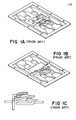
- Figures 1 and 2 show optocouplers which are fabricated according to the prior art.
- Figures 1A-C illustrate two 90° folding steps, described in U.S. Patent No. 4,446,375, which have been used in the manufacture of prior art optocouplers to align the LED and the photodiode.
- Figure 2 shows an optocoupler, described in U.S. Patent No. 3,925,801, which uses the thickness of a single dielectric sheet compressed between the LED and the photodiode dice to establish the size of the isolation gap.
- FIG 3 shows a lead frame 1 which is used in the assembly of an optical isolator in accordance with the preferred embodiment of the present invention.
- the lead frame 1 is 0,254mm (.010 inch) thick and is fabricated from alloy 42 (42% nickel, 58% iron) in a well known manner.
- the hatched regions are plated with gold to facilitate later die attach and wire bond operations and for the sake of clarity these plated regions are not shown in the other Figures.
- Two side rails 3 and 5 provide longitudinal stability for the lead frame 1 which is approximately 213,36mm (8.4 inches) in length and one inch in width. Repeated tie rails 21 and 23 provide lateral stability to the lead frame 1.
- each alternating LED sections 11 and photodiode sections 13 are located on lead frame 1 and each individual section is divided about arms 17 and seats 19 into identical left and right halves.
- the LED sections 11 are attached to side rails 3 and 5 by 0,3556mm (.014 inch) wide hinge pins 31, 33 and the photodiode sections 13 are attached to side rails 3 and 5 by dam bar ends 35, 37.
- each left pair of LED sections 11 and photodiode sections 13 will be combined to form one optical isolator.
- Each right pair will be combined into one optical isolator in a like manner.
- a total of twenty optical isolators in standard integrated circuit 8-lead packages will be fabricated upon the single lead frame 1.
- Figures 4A-B are a flow chart of the various assembly steps which are performed during the manufacture of an optical isolator in accordance with the present invention.
- the individual assembly steps for a single optical isolator 103 are discussed below in connection with Figures 5-11. During automated assembly all of the optical isolators on the lead frame 1 would be fabricated sequentially.
- Figure 5 shows the lead frame 1 after performance of step 41 in which attachment portions 81 and 83 are down set below the plane of side rails 3 and 5.
- the down set operation may easily be performed using well known stamping techniques and the amount of down set is predetermined to set the size of the isolation gap.
- each of the attachment portions 81, 83 was down set a distance of 0,4826mm (.019 inch) although this downset distance may vary with the thickness of different LED and photodiode dice.
- the seat 19 is down set by an amount equal to the thickness of the arm 17, i.e., 0,254mm (.010 inch), to set coplanar alignment of the LED section 11 with the photodiode section 13 after rotation by allowing the arm 17 to rest against the down set area of the seat 19. After rotation is completed, the two sections 81 and 83 will be located equidistantly above and below the plane of the side rails 3, 5.
- FIG. 6 shows steps 43 and 45 in which the die attach and wire bond operations are performed upon lead frame 1 in a conventional manner.
- An LED die 91 and an optional buffer die 93 are attached to an LED lead 95 and a photodiode die 97 is attached to a photodiode lead 99.
- Various bond wires are attached to the other leads shown as required.
- the LED 91 is a high speed gallium arsenide phosphide device of the type described in U.S. Patent No. 3,836,793 which is incorporated herein by reference.
- the LED 91 has a thickness of approximately 0,1524mm (.006 inch) and the photodiode 97 has a thickness of approximately 0,3048mm (.012 inch).
- FIG 7 shows the first of the combination steps 47 which are outlined in greater detail in the flow chart of Figure 48. For the sake of clarity, only the left section of the lead frame 1 is shown in Figures 7-9.
- combination operation step 61 the tie rail 21 of LED section 11 is severed from both of the side rails 3 and 5. This leaves the LED section 11 attached only at the laterally aligned hinge pins 31, 33 and longitudinal rotation about the hinge pins is possible.
- the dam bar ends 35 and 37 of the photodiode section 13 are not severed and, consequently, the photodiode section 13 remains rigidly attached to the side rails 3 and 5.
- step 63 the LED section 11 is rotated approximately 15° upwards about the hinge pins 31 and 33.
- the rotational movements of steps 63-69 may be made in a single step or in multiple steps as required for the particular combination apparatus used.
- the lead frame 1 is configured for a standard 8-lead package, standard integrated circuit processing equipment may be used.
- persons of ordinary skill in the art will be well able to reconfigure the lead frame 1 to allow rotation of the photodiode section 13 instead of rotation of the LED section 11.
- FIG. 8 shows step 65 in which the LED section 11 is rotated to approximately 90° relative to the plane of the side rails 3, 5.
- step 67 (not shown), the LED section 11 is rotated to approximately 165°.
- the entire 180° rotation could be performed in a single step instead of in the multiple steps used in the preferred embodiment.
- Figure 9 shows step 69 in which pressure pads of the combination apparatus press the LED section 11 to a fully 180° rotated position coplanar with side rails 3, 5 and photodiode section 13.
- the arm 17 is seated against the down set area of the seat 19 and damage to the two dice may be avoided if the lead frame 1 is accidentally bumped.
- the arm 17 and the seat 19 may be spot welded together to provide additional stability during transfer molding. Since, unlike certain prior art devices, the size of the isolation gap is not set by compression of a dielectric sheet between the dice 91, 97 damage to the dice 91, 97 does not occur.
- each of hinge pins 31, 33 must be greater than the thickness of side rails 3 and 5 so that swaging can occur. But, the hinge pins 31, 33 widths must not be so great that excessive material cold flows during stamping thereby causing buckling or deformation of portions of the lead frame 1. In the preferred embodiment, widths in the range of 0,3048mm (.012inch) to 0,4064mm (.016inch) were used.
- Figure 10 shows a close-up cross sectional view of the optical isolator 103 after completion of the step 47.
- the LED 91 is positioned correctly over the photodiode 97 across an isolation gap 101.
- the size of the isolation gap 101 is determined in step 41 by the amount of down set of attachment portions 81, 83 and seat 19 and by the thicknesses of the dice 91 and 97.
- the leads 95 and 99 are coplanar which permits the use of standard transfer molding apparatus in step 53 and eliminates flashing on the bond leads during molding.
- FIG 11 shows steps 49-55 in which final packaging of the optical isolator 103 is performed.
- two dielectric sheets 111, 113 are attached to the outer surfaces of leads 95 and 99.
- Sheets 111, 113 may be made from any nonconductive material such as 0,07112mm (.0028 inch) thick commercially available DuPont Company Kapton tape which is cut to 2,54 by 2,54mm (.100 by .100 inch) in size and which has an adhesive coating on one side.
- an optically transmissive silicone resin such as Dow Corning Company's Hipec Ql-4939 semiconductor protective coating is injected into the isolation gap 101 between sheets 111 and 113 to form a light guide 115.
- the sheets 111, 113 limit the resin flow to the desired location and preclude structural weakening of the optical isolator 103 which could be caused by excessive resin flow.
- the resin effectively encapsulates the dice 91, 93, 97 within the light guide 115 and thereby reduces the risk of damage to the optical isolator 103 during thermal shock or temperature cycling.
- step 53 standard transfer molding techniques are used to encapsulate the entire optical isolator 103 in an opaque package 117 of, e.g., Nitto Electric Industrial Co. MP-101S transfer molding compound.
- step 55 all of the leads including leads 95 and 99 are cut from side rails 3, 5 and tie rails 21, 23 and the leads are bent to the desired packaged shape.
- Figure 12 shows an alternate preferred embodiment of the present invention in which a dielectric sheet 131 is positioned within the isolation gap 101 between dice 91, 97.
- Figure 13 is a flow chart of the assembly of the optical isolator 121 shown in Figure 12 using a number of steps common to the flow chart of Figure 4A.
- step 151 the sheet 113 shown in Figure 11 or any other rigid material sheet is attached to the lead 99 using the adhesive layer on the upper surface of the sheet 113.
- step a second dielectric sheet 131 is placed on top of the die 97 touching the end of sheet 113 and adhering to the adhesive layer thereon so that the sheet 131 is angled away from the bond wires thereby avoiding damage to the bond wires.
- the tilted angling of sheet 131 creates a wedge shaped cavity between the sheet 131 and the die 97 in which resin 133 is contained in the desired position for transmitting light to the photodiode die 97.
- the sheet 131 is 3,175mm by 3,175mm (.125 inch by .125 inch) in size and may be fabricated from a piece of DuPont Company FEP number 200C20 material.
- step 155 resin 133, discussed above with reference to Figure 11, is applied between the sheet 131 and the die 97 and in step 157 the resin is briefly cured to attain a gel consistency.
- Performance of the combination operations of step 47 does not result in damage to the dice 91, 97 because the size of the isolation gap 101 is determined by the amount of down set and not by compression of the sheet 131 between the dice 91, 97 as is often done in the prior art. Damage to the bond wires is avoided since the sheet 131 rests against the sheet 113 and the edge of die 97 and is thereby tilted at an angle and avoids contact with the bond wires.
- step 161 additional resin 133 is applied between the sheet 131 and the die 91. The resin is cured to a gel consistency in step 163 and it is completely cured in step 165 before final steps 53, 55 are performed.
- the sheet 131 has the effect of increasing the breakdown voltage of the optical isolator 121 since it has a greater breakdown voltage than does the resin 133. It also serves to increase the length of any air gap present at the interface between the resin 133 and the molding compound 117 and minimizes the effect of air bubbles within the resin 133.
- the angled presence of the sheet 131 creates a properly positioned and resin filled wedge shaped cavity which conducts light between the die 91, 97 and which also allows a smaller amount of resin 133 to be used so that the amount of resin that may wet the leads 95, 99 is reduced. This decrease in lead wetting results in the attainment of superior moisture penetration resistance properties by the optical isolator 121.
Abstract
Description
- An optical isolator may be used in an electrical circuit to allow signal propagation in a forward direction while maintaining voltage and current isolation between the input and the output of the optical isolator. Such an isolator includes a light emitting diode (LED) at the input, a photodiode at the output and an optically transmissive high breakdown voltage isolation gap separating the LED and the photodiode. In order to achieve optimum isolator performance the size of the isolation gap and the alignment of the LED and the photodiode must be maintained accurately during manufacture.
- One prior art attempt to automate optical isolator manufacture, described in U.S. Patent No. 4,446,375 and shown in Figures 1A-C hereof, has been to align the LED and the photodiode during fabrication by folding the LED lead and the separate LED bond lead into place over the detector in two ninety degree steps. Although the use of such a folded lead frame technique decreases the assembly time for each isolator a complex folding apparatus is required to make the two 90° folds which lie along different axes and errors in the placement of the folds may affect the accuracy of the LED-photodiode alignment. During folding, damage to the bond wires may occur because the LED lead and the LED bond lead are not securely attached together and because the dielectric sheet between the LED and the photodiode dice is free to rest against and damage the LED and photodiode bond wires. As additionally described in U.S. Patent No. 3,925,801 and shown in Figure 2 hereof, the size of the isolation gap in many prior art optical isolators is determined by the thickness of a dielectric sheet located between the LED and the photodiode. The insertion of such a sheet during manufacture has often resulted in bond wire damage.
- In accordance with the illustrated preferred embodiment of the present invention, an optical isolator is manufactured simply and repeatably using standard form lead frames. Prior to die attachment and wire bonding of the optical isolator, the LED and photodiode attachment portions of the lead frame are displaced to a common plane located below the plane of the remainder of the lead frame. The entire LED section of the lead frame is then rotated 180 degrees about a pair of hinge pins until it is coplanar with the photodiode section of the lead frame. After rotation is completed the hinge pins are stamped to eliminate spring back of the rotated LED section of the lead frame. A clear resin is injected between two dielectric sheets attached to the outer surfaces of the LED and photodiode leads to form a light guide between the LED and the photodiode. The optical isolator is encapsulated and the protruding leads are cut and bent to the desired final package shape. In an alternate preferred embodiment of the present invention, a first dielectric sheet is attached to the outer surface of either the LED or the photodiode lead and a second dielectric sheet is positioned between the LED and the photodiode dice. The second sheet rests upon (and adheres to adhesive on) the first sheet and extends between the dice at an angle so that damage to the dice and to the bond wires is avoided.
- Other features and advantages of the present invention will appear from the following description.
- Figures 1A-C show a prior art optocoupler having a folded lead frame construction.
- Figure 2 shows a prior art optocoupler having a dielectric sheet compressed between the LED and the photodiode.
- Figure 3 shows an optical isolator lead frame in accordance with the preferred embodiment of the present invention.
- Figures 4A-B are a flow chart of the optical isolator assembly steps in accordance with the preferred embodiment of the present invention.
- Figures 5-11 show various stages in. the assembly of the optical isolator in accordance with the flow chart of Figure 4.
- Figure 12 shows an alternate preferred embodiment of the present invention in which a dielectric sheet is positioned between the LED and photodiode dice at a tilted angle.
- Figure 13 is a flow chart of the assembly steps of the alternate preferred embodiment shown in Figure 12.
- Figures 1 and 2 show optocouplers which are fabricated according to the prior art. Figures 1A-C illustrate two 90° folding steps, described in U.S. Patent No. 4,446,375, which have been used in the manufacture of prior art optocouplers to align the LED and the photodiode. Figure 2 shows an optocoupler, described in U.S. Patent No. 3,925,801, which uses the thickness of a single dielectric sheet compressed between the LED and the photodiode dice to establish the size of the isolation gap.
- Figure 3 shows a
lead frame 1 which is used in the assembly of an optical isolator in accordance with the preferred embodiment of the present invention. Thelead frame 1 is 0,254mm (.010 inch) thick and is fabricated from alloy 42 (42% nickel, 58% iron) in a well known manner. The hatched regions are plated with gold to facilitate later die attach and wire bond operations and for the sake of clarity these plated regions are not shown in the other Figures. Twoside rails lead frame 1 which is approximately 213,36mm (8.4 inches) in length and one inch in width. Repeatedtie rails lead frame 1. Ten eachalternating LED sections 11 andphotodiode sections 13 are located onlead frame 1 and each individual section is divided aboutarms 17 andseats 19 into identical left and right halves. TheLED sections 11 are attached toside rails wide hinge pins photodiode sections 13 are attached toside rails dam bar ends LED sections 11 andphotodiode sections 13 will be combined to form one optical isolator. Each right pair will be combined into one optical isolator in a like manner. A total of twenty optical isolators in standard integrated circuit 8-lead packages will be fabricated upon thesingle lead frame 1. - Figures 4A-B are a flow chart of the various assembly steps which are performed during the manufacture of an optical isolator in accordance with the present invention. The individual assembly steps for a single
optical isolator 103 are discussed below in connection with Figures 5-11. During automated assembly all of the optical isolators on thelead frame 1 would be fabricated sequentially. - Figure 5 shows the
lead frame 1 after performance ofstep 41 in whichattachment portions side rails attachment portions seat 19 is down set by an amount equal to the thickness of thearm 17, i.e., 0,254mm (.010 inch), to set coplanar alignment of theLED section 11 with thephotodiode section 13 after rotation by allowing thearm 17 to rest against the down set area of theseat 19. After rotation is completed, the twosections side rails - Figure 6 shows
steps lead frame 1 in a conventional manner. AnLED die 91 and an optional buffer die 93 are attached to anLED lead 95 and a photodiode die 97 is attached to aphotodiode lead 99. Various bond wires are attached to the other leads shown as required. TheLED 91 is a high speed gallium arsenide phosphide device of the type described in U.S. Patent No. 3,836,793 which is incorporated herein by reference. TheLED 91 has a thickness of approximately 0,1524mm (.006 inch) and thephotodiode 97 has a thickness of approximately 0,3048mm (.012 inch). - Figure 7 shows the first of the
combination steps 47 which are outlined in greater detail in the flow chart of Figure 48. For the sake of clarity, only the left section of thelead frame 1 is shown in Figures 7-9. Incombination operation step 61, thetie rail 21 ofLED section 11 is severed from both of theside rails LED section 11 attached only at the laterally alignedhinge pins photodiode section 13 are not severed and, consequently, thephotodiode section 13 remains rigidly attached to theside rails - In
step 63, theLED section 11 is rotated approximately 15° upwards about thehinge pins lead frame 1 is configured for a standard 8-lead package, standard integrated circuit processing equipment may be used. Of course, persons of ordinary skill in the art will be well able to reconfigure thelead frame 1 to allow rotation of thephotodiode section 13 instead of rotation of theLED section 11. - Figure 8 shows
step 65 in which theLED section 11 is rotated to approximately 90° relative to the plane of theside rails LED section 11 is rotated to approximately 165°. Of course, the entire 180° rotation could be performed in a single step instead of in the multiple steps used in the preferred embodiment. - Figure 9 shows
step 69 in which pressure pads of the combination apparatus press theLED section 11 to a fully 180° rotated position coplanar withside rails photodiode section 13. At this point, thearm 17 is seated against the down set area of theseat 19 and damage to the two dice may be avoided if thelead frame 1 is accidentally bumped. Thearm 17 and theseat 19 may be spot welded together to provide additional stability during transfer molding. Since, unlike certain prior art devices, the size of the isolation gap is not set by compression of a dielectric sheet between thedice dice - In order to prevent rotational spring back of the
LED section 11 from the 180° rotated position the two hinge pins 31, 33 are stamped and thereby flattened. The width of each of hinge pins 31, 33 must be greater than the thickness ofside rails lead frame 1. In the preferred embodiment, widths in the range of 0,3048mm (.012inch) to 0,4064mm (.016inch) were used. - Figure 10 shows a close-up cross sectional view of the
optical isolator 103 after completion of thestep 47. TheLED 91 is positioned correctly over thephotodiode 97 across anisolation gap 101. The size of theisolation gap 101 is determined instep 41 by the amount of down set ofattachment portions seat 19 and by the thicknesses of thedice step 53 and eliminates flashing on the bond leads during molding. - Figure 11 shows steps 49-55 in which final packaging of the
optical isolator 103 is performed. Instep 49, twodielectric sheets leads Sheets isolation gap 101 betweensheets light guide 115. By using surface tension forces, thesheets optical isolator 103 which could be caused by excessive resin flow. The resin effectively encapsulates thedice light guide 115 and thereby reduces the risk of damage to theoptical isolator 103 during thermal shock or temperature cycling. - In
step 53, standard transfer molding techniques are used to encapsulate the entireoptical isolator 103 in anopaque package 117 of, e.g., Nitto Electric Industrial Co. MP-101S transfer molding compound. Finally, instep 55, all of the leads including leads 95 and 99 are cut fromside rails - Figure 12 shows an alternate preferred embodiment of the present invention in which a
dielectric sheet 131 is positioned within theisolation gap 101 betweendice optical isolator 121 shown in Figure 12 using a number of steps common to the flow chart of Figure 4A. Instep 151 thesheet 113 shown in Figure 11 or any other rigid material sheet is attached to thelead 99 using the adhesive layer on the upper surface of thesheet 113. In step 153 asecond dielectric sheet 131 is placed on top of the die 97 touching the end ofsheet 113 and adhering to the adhesive layer thereon so that thesheet 131 is angled away from the bond wires thereby avoiding damage to the bond wires. The tilted angling ofsheet 131 creates a wedge shaped cavity between thesheet 131 and the die 97 in whichresin 133 is contained in the desired position for transmitting light to the photodiode die 97. Thesheet 131 is 3,175mm by 3,175mm (.125 inch by .125 inch) in size and may be fabricated from a piece of DuPont Company FEP number 200C20 material. - In
step 155resin 133, discussed above with reference to Figure 11, is applied between thesheet 131 and thedie 97 and instep 157 the resin is briefly cured to attain a gel consistency. Performance of the combination operations ofstep 47 does not result in damage to thedice isolation gap 101 is determined by the amount of down set and not by compression of thesheet 131 between thedice sheet 131 rests against thesheet 113 and the edge ofdie 97 and is thereby tilted at an angle and avoids contact with the bond wires. Instep 161,additional resin 133 is applied between thesheet 131 and thedie 91. The resin is cured to a gel consistency instep 163 and it is completely cured instep 165 beforefinal steps - The
sheet 131 has the effect of increasing the breakdown voltage of theoptical isolator 121 since it has a greater breakdown voltage than does theresin 133. It also serves to increase the length of any air gap present at the interface between theresin 133 and themolding compound 117 and minimizes the effect of air bubbles within theresin 133. The angled presence of thesheet 131 creates a properly positioned and resin filled wedge shaped cavity which conducts light between the die 91, 97 and which also allows a smaller amount ofresin 133 to be used so that the amount of resin that may wet theleads optical isolator 121.
Claims (45)
Applications Claiming Priority (2)
| Application Number | Priority Date | Filing Date | Title |
|---|---|---|---|
| US748520 | 1985-06-25 | ||
| US06/748,520 US4694183A (en) | 1985-06-25 | 1985-06-25 | Optical isolator fabricated upon a lead frame |
Publications (3)
| Publication Number | Publication Date |
|---|---|
| EP0206325A2 true EP0206325A2 (en) | 1986-12-30 |
| EP0206325A3 EP0206325A3 (en) | 1989-03-15 |
| EP0206325B1 EP0206325B1 (en) | 1992-03-25 |
Family
ID=25009800
Family Applications (1)
| Application Number | Title | Priority Date | Filing Date |
|---|---|---|---|
| EP86108623A Expired - Lifetime EP0206325B1 (en) | 1985-06-25 | 1986-06-25 | Method for fabricating an optical isolator. |
Country Status (4)
| Country | Link |
|---|---|
| US (1) | US4694183A (en) |
| EP (1) | EP0206325B1 (en) |
| JP (1) | JPH084148B2 (en) |
| DE (1) | DE3684519D1 (en) |
Cited By (4)
| Publication number | Priority date | Publication date | Assignee | Title |
|---|---|---|---|---|
| EP0276749A1 (en) * | 1987-01-26 | 1988-08-03 | Siemens Aktiengesellschaft | Optoelectronic coupling element |
| EP0513908A2 (en) * | 1991-05-17 | 1992-11-19 | Koninklijke Philips Electronics N.V. | Opto-electronic coupler |
| US7291905B2 (en) | 2000-08-08 | 2007-11-06 | Nec Electronics Corporation | Lead frame, semiconductor device produced by using the same and method of producing the semiconductor device |
| CN103021892A (en) * | 2012-12-28 | 2013-04-03 | 日月光半导体(昆山)有限公司 | Leadless semiconductor package, method for manufacturing the same, and lead frame strip |
Families Citing this family (14)
| Publication number | Priority date | Publication date | Assignee | Title |
|---|---|---|---|---|
| DE3713067A1 (en) * | 1986-09-30 | 1988-03-31 | Siemens Ag | OPTOELECTRONIC COUPLING ELEMENT AND METHOD FOR THE PRODUCTION THEREOF |
| US4980568A (en) * | 1989-05-22 | 1990-12-25 | Hewlett-Packard Company | Optical isolator having high voltage isolation and high light flux light guide |
| SG52794A1 (en) * | 1990-04-26 | 1998-09-28 | Hitachi Ltd | Semiconductor device and method for manufacturing same |
| JPH0749815Y2 (en) * | 1990-07-23 | 1995-11-13 | シャープ株式会社 | Surface mount type optical coupling device |
| JPH0621293A (en) * | 1992-06-29 | 1994-01-28 | Rohm Co Ltd | Axial lead frame |
| JP2004087802A (en) * | 2002-08-27 | 2004-03-18 | Fujitsu Ltd | Optical communication apparatus |
| JP4897530B2 (en) * | 2007-03-23 | 2012-03-14 | ルネサスエレクトロニクス株式会社 | Photocoupler and its assembly method |
| JP5088059B2 (en) * | 2007-09-18 | 2012-12-05 | 富士電機株式会社 | Isolator and method of manufacturing isolator |
| CN101458366B (en) * | 2007-12-13 | 2010-12-01 | 旭丽电子(广州)有限公司 | Optical coupler wire guide frame band |
| TWI416684B (en) * | 2010-02-02 | 2013-11-21 | Everlight Electronics Co Ltd | Double-sided leadframe structure |
| US20130168553A1 (en) * | 2012-01-03 | 2013-07-04 | Avago Technologies Ecbu Ip (Singapore) Pte. Ltd. | Thermally-Sensitive Optocoupler |
| US9029818B2 (en) * | 2012-06-21 | 2015-05-12 | Avago Technologies General Ip (Singapore) Pte. Ltd. | Optoelectronic device and method of manufacture |
| US10283699B2 (en) * | 2016-01-29 | 2019-05-07 | Avago Technologies International Sales Pte. Limited | Hall-effect sensor isolator |
| TWI630430B (en) * | 2017-07-26 | 2018-07-21 | 茂達電子股份有限公司 | Optocoupler device and frame module thereof |
Citations (6)
| Publication number | Priority date | Publication date | Assignee | Title |
|---|---|---|---|---|
| FR2176103A1 (en) * | 1972-03-15 | 1973-10-26 | Motorola Inc | |
| DE2304148A1 (en) * | 1973-01-29 | 1974-08-01 | Siemens Ag | OPTOELECTRONIC COMPONENT |
| US3839782A (en) * | 1972-03-15 | 1974-10-08 | M Lincoln | Method for using a lead frame for the manufacture of electric devices having semiconductor chips placed in a face-to-face relation |
| US3893158A (en) * | 1972-03-15 | 1975-07-01 | Motorola Inc | Lead frame for the manufacture of electric devices having semiconductor chips placed in a face to face relation |
| US4047045A (en) * | 1975-03-03 | 1977-09-06 | Paxton Jr Grady W | Optical coupler |
| GB2107929A (en) * | 1981-10-14 | 1983-05-05 | Gen Electric | Optocouplers |
Family Cites Families (5)
| Publication number | Priority date | Publication date | Assignee | Title |
|---|---|---|---|---|
| US3660669A (en) * | 1970-04-15 | 1972-05-02 | Motorola Inc | Optical coupler made by juxtaposition of lead frame mounted sensor and light emitter |
| GB1423779A (en) * | 1972-02-14 | 1976-02-04 | Hewlett Packard Co | Photon isolators |
| GB1557685A (en) * | 1976-02-02 | 1979-12-12 | Fairchild Camera Instr Co | Optically coupled isolator device |
| JPS57143889A (en) * | 1981-03-02 | 1982-09-06 | Toshiba Corp | Photo-coupling semiconductor device |
| JPS57197880A (en) * | 1981-05-29 | 1982-12-04 | Toshiba Corp | Photo coupling semiconductor device |
-
1985
- 1985-06-25 US US06/748,520 patent/US4694183A/en not_active Expired - Lifetime
-
1986
- 1986-06-25 DE DE8686108623T patent/DE3684519D1/en not_active Expired - Lifetime
- 1986-06-25 JP JP61149299A patent/JPH084148B2/en not_active Expired - Lifetime
- 1986-06-25 EP EP86108623A patent/EP0206325B1/en not_active Expired - Lifetime
Patent Citations (6)
| Publication number | Priority date | Publication date | Assignee | Title |
|---|---|---|---|---|
| FR2176103A1 (en) * | 1972-03-15 | 1973-10-26 | Motorola Inc | |
| US3839782A (en) * | 1972-03-15 | 1974-10-08 | M Lincoln | Method for using a lead frame for the manufacture of electric devices having semiconductor chips placed in a face-to-face relation |
| US3893158A (en) * | 1972-03-15 | 1975-07-01 | Motorola Inc | Lead frame for the manufacture of electric devices having semiconductor chips placed in a face to face relation |
| DE2304148A1 (en) * | 1973-01-29 | 1974-08-01 | Siemens Ag | OPTOELECTRONIC COMPONENT |
| US4047045A (en) * | 1975-03-03 | 1977-09-06 | Paxton Jr Grady W | Optical coupler |
| GB2107929A (en) * | 1981-10-14 | 1983-05-05 | Gen Electric | Optocouplers |
Cited By (6)
| Publication number | Priority date | Publication date | Assignee | Title |
|---|---|---|---|---|
| EP0276749A1 (en) * | 1987-01-26 | 1988-08-03 | Siemens Aktiengesellschaft | Optoelectronic coupling element |
| EP0513908A2 (en) * | 1991-05-17 | 1992-11-19 | Koninklijke Philips Electronics N.V. | Opto-electronic coupler |
| EP0513908A3 (en) * | 1991-05-17 | 1993-03-17 | N.V. Philips' Gloeilampenfabrieken | Opto-electronic coupler |
| US7291905B2 (en) | 2000-08-08 | 2007-11-06 | Nec Electronics Corporation | Lead frame, semiconductor device produced by using the same and method of producing the semiconductor device |
| CN103021892A (en) * | 2012-12-28 | 2013-04-03 | 日月光半导体(昆山)有限公司 | Leadless semiconductor package, method for manufacturing the same, and lead frame strip |
| CN103021892B (en) * | 2012-12-28 | 2016-05-11 | 日月光半导体(昆山)有限公司 | Leadless semiconductor package, method for manufacturing the same, and lead frame strip |
Also Published As
| Publication number | Publication date |
|---|---|
| EP0206325B1 (en) | 1992-03-25 |
| US4694183A (en) | 1987-09-15 |
| EP0206325A3 (en) | 1989-03-15 |
| DE3684519D1 (en) | 1992-04-30 |
| JPS6236883A (en) | 1987-02-17 |
| JPH084148B2 (en) | 1996-01-17 |
Similar Documents
| Publication | Publication Date | Title |
|---|---|---|
| US5049527A (en) | Optical isolator | |
| US5148243A (en) | Optical isolator with encapsulation | |
| EP0206325B1 (en) | Method for fabricating an optical isolator. | |
| US6072228A (en) | Multi-part lead frame with dissimilar materials and method of manufacturing | |
| US5696033A (en) | Method for packaging a semiconductor die | |
| US5834691A (en) | Lead frame, its use in the fabrication of resin-encapsulated semiconductor device | |
| US7863107B2 (en) | Semiconductor device and manufacturing method of the same | |
| EP0502710A1 (en) | Flexible film semiconductor package | |
| US6454158B1 (en) | Wire bonding apparatus and wire bonding method of semiconductor device | |
| US5923081A (en) | Compression layer on the leadframe to reduce stress defects | |
| US4863806A (en) | Optical isolator | |
| JPH11121543A (en) | Chip scale package | |
| US8975119B2 (en) | Manufacturing method of semiconductor device | |
| JPH09172033A (en) | Semiconductor device and manufacture thereof | |
| KR100304922B1 (en) | Lead frame and semiconductor package with such lead frame | |
| JPH0366152A (en) | Semiconductor integrated circuit module | |
| EP0807972A2 (en) | Semiconductor device and method of its fabrication | |
| JP3185455B2 (en) | Resin-sealed semiconductor device | |
| JP3293757B2 (en) | Method of manufacturing lead frame assembly for manufacturing semiconductor device | |
| EP0410116A2 (en) | Method of manufacturing a wire-bonded semiconductor device | |
| JPH05291486A (en) | Resin-sealed semiconductor device | |
| JPH07120728B2 (en) | Semiconductor device and manufacturing method thereof | |
| JPH10163382A (en) | Semiconductor package and its manufacture | |
| JPH0666399B2 (en) | Lead frame |
Legal Events
| Date | Code | Title | Description |
|---|---|---|---|
| PUAI | Public reference made under article 153(3) epc to a published international application that has entered the european phase |
Free format text: ORIGINAL CODE: 0009012 |
|
| AK | Designated contracting states |
Kind code of ref document: A2 Designated state(s): DE FR GB |
|
| PUAL | Search report despatched |
Free format text: ORIGINAL CODE: 0009013 |
|
| AK | Designated contracting states |
Kind code of ref document: A3 Designated state(s): DE FR GB |
|
| 17P | Request for examination filed |
Effective date: 19890905 |
|
| 17Q | First examination report despatched |
Effective date: 19901102 |
|
| GRAA | (expected) grant |
Free format text: ORIGINAL CODE: 0009210 |
|
| AK | Designated contracting states |
Kind code of ref document: B1 Designated state(s): DE FR GB |
|
| REF | Corresponds to: |
Ref document number: 3684519 Country of ref document: DE Date of ref document: 19920430 |
|
| ET | Fr: translation filed | ||
| PLBE | No opposition filed within time limit |
Free format text: ORIGINAL CODE: 0009261 |
|
| STAA | Information on the status of an ep patent application or granted ep patent |
Free format text: STATUS: NO OPPOSITION FILED WITHIN TIME LIMIT |
|
| 26N | No opposition filed | ||
| PGFP | Annual fee paid to national office [announced via postgrant information from national office to epo] |
Ref country code: FR Payment date: 19950526 Year of fee payment: 10 |
|
| PGFP | Annual fee paid to national office [announced via postgrant information from national office to epo] |
Ref country code: GB Payment date: 19960529 Year of fee payment: 11 |
|
| PG25 | Lapsed in a contracting state [announced via postgrant information from national office to epo] |
Ref country code: FR Effective date: 19970228 |
|
| REG | Reference to a national code |
Ref country code: FR Ref legal event code: ST |
|
| PG25 | Lapsed in a contracting state [announced via postgrant information from national office to epo] |
Ref country code: GB Free format text: LAPSE BECAUSE OF NON-PAYMENT OF DUE FEES Effective date: 19970625 |
|
| GBPC | Gb: european patent ceased through non-payment of renewal fee |
Effective date: 19970625 |
|
| PGFP | Annual fee paid to national office [announced via postgrant information from national office to epo] |
Ref country code: DE Payment date: 20050801 Year of fee payment: 20 |