EP0201037B1 - Method for etching openings with a controlled wall profile - Google Patents
Method for etching openings with a controlled wall profile Download PDFInfo
- Publication number
- EP0201037B1 EP0201037B1 EP86105947A EP86105947A EP0201037B1 EP 0201037 B1 EP0201037 B1 EP 0201037B1 EP 86105947 A EP86105947 A EP 86105947A EP 86105947 A EP86105947 A EP 86105947A EP 0201037 B1 EP0201037 B1 EP 0201037B1
- Authority
- EP
- European Patent Office
- Prior art keywords
- layer
- opening
- etching
- silicon dioxide
- chf3
- Prior art date
- Legal status (The legal status is an assumption and is not a legal conclusion. Google has not performed a legal analysis and makes no representation as to the accuracy of the status listed.)
- Expired
Links
- 238000000034 method Methods 0.000 title claims description 37
- 238000005530 etching Methods 0.000 title claims description 24
- VYPSYNLAJGMNEJ-UHFFFAOYSA-N Silicium dioxide Chemical compound O=[Si]=O VYPSYNLAJGMNEJ-UHFFFAOYSA-N 0.000 claims description 53
- 235000012239 silicon dioxide Nutrition 0.000 claims description 26
- 239000000377 silicon dioxide Substances 0.000 claims description 26
- 229920002120 photoresistant polymer Polymers 0.000 claims description 23
- XPDWGBQVDMORPB-UHFFFAOYSA-N Fluoroform Chemical compound FC(F)F XPDWGBQVDMORPB-UHFFFAOYSA-N 0.000 claims description 21
- 238000001020 plasma etching Methods 0.000 claims description 13
- 230000003247 decreasing effect Effects 0.000 claims description 5
- 239000007789 gas Substances 0.000 description 25
- 229960001866 silicon dioxide Drugs 0.000 description 15
- 239000004215 Carbon black (E152) Substances 0.000 description 12
- 229930195733 hydrocarbon Natural products 0.000 description 12
- 150000002430 hydrocarbons Chemical class 0.000 description 12
- 229910052681 coesite Inorganic materials 0.000 description 6
- 229910052906 cristobalite Inorganic materials 0.000 description 6
- 239000000203 mixture Substances 0.000 description 6
- 229910052682 stishovite Inorganic materials 0.000 description 6
- 229910052905 tridymite Inorganic materials 0.000 description 6
- 229910052581 Si3N4 Inorganic materials 0.000 description 5
- 239000002184 metal Substances 0.000 description 5
- HQVNEWCFYHHQES-UHFFFAOYSA-N silicon nitride Chemical compound N12[Si]34N5[Si]62N3[Si]51N64 HQVNEWCFYHHQES-UHFFFAOYSA-N 0.000 description 5
- XUIMIQQOPSSXEZ-UHFFFAOYSA-N Silicon Chemical compound [Si] XUIMIQQOPSSXEZ-UHFFFAOYSA-N 0.000 description 4
- 239000010703 silicon Substances 0.000 description 4
- 239000004020 conductor Substances 0.000 description 3
- 230000007423 decrease Effects 0.000 description 3
- 239000001257 hydrogen Substances 0.000 description 3
- 229910052739 hydrogen Inorganic materials 0.000 description 3
- 229910052710 silicon Inorganic materials 0.000 description 3
- UFHFLCQGNIYNRP-UHFFFAOYSA-N Hydrogen Chemical compound [H][H] UFHFLCQGNIYNRP-UHFFFAOYSA-N 0.000 description 2
- 230000015556 catabolic process Effects 0.000 description 2
- 239000003153 chemical reaction reagent Substances 0.000 description 2
- 230000007547 defect Effects 0.000 description 2
- 238000004519 manufacturing process Methods 0.000 description 2
- 239000000463 material Substances 0.000 description 2
- 238000001465 metallisation Methods 0.000 description 2
- 229910052814 silicon oxide Inorganic materials 0.000 description 2
- QVGXLLKOCUKJST-UHFFFAOYSA-N atomic oxygen Chemical compound [O] QVGXLLKOCUKJST-UHFFFAOYSA-N 0.000 description 1
- 229910052731 fluorine Inorganic materials 0.000 description 1
- 239000011737 fluorine Substances 0.000 description 1
- 125000001153 fluoro group Chemical group F* 0.000 description 1
- NBVXSUQYWXRMNV-UHFFFAOYSA-N fluoromethane Chemical compound FC NBVXSUQYWXRMNV-UHFFFAOYSA-N 0.000 description 1
- 239000001307 helium Substances 0.000 description 1
- 229910052734 helium Inorganic materials 0.000 description 1
- SWQJXJOGLNCZEY-UHFFFAOYSA-N helium atom Chemical compound [He] SWQJXJOGLNCZEY-UHFFFAOYSA-N 0.000 description 1
- 150000002431 hydrogen Chemical class 0.000 description 1
- 239000011810 insulating material Substances 0.000 description 1
- 238000010849 ion bombardment Methods 0.000 description 1
- 150000002500 ions Chemical class 0.000 description 1
- 239000001301 oxygen Substances 0.000 description 1
- 229910052760 oxygen Inorganic materials 0.000 description 1
- 239000005360 phosphosilicate glass Substances 0.000 description 1
- 239000004065 semiconductor Substances 0.000 description 1
- 239000007787 solid Substances 0.000 description 1
Images
Classifications
-
- H—ELECTRICITY
- H01—ELECTRIC ELEMENTS
- H01L—SEMICONDUCTOR DEVICES NOT COVERED BY CLASS H10
- H01L21/00—Processes or apparatus adapted for the manufacture or treatment of semiconductor or solid state devices or of parts thereof
- H01L21/02—Manufacture or treatment of semiconductor devices or of parts thereof
- H01L21/04—Manufacture or treatment of semiconductor devices or of parts thereof the devices having potential barriers, e.g. a PN junction, depletion layer or carrier concentration layer
- H01L21/18—Manufacture or treatment of semiconductor devices or of parts thereof the devices having potential barriers, e.g. a PN junction, depletion layer or carrier concentration layer the devices having semiconductor bodies comprising elements of Group IV of the Periodic Table or AIIIBV compounds with or without impurities, e.g. doping materials
- H01L21/30—Treatment of semiconductor bodies using processes or apparatus not provided for in groups H01L21/20 - H01L21/26
- H01L21/31—Treatment of semiconductor bodies using processes or apparatus not provided for in groups H01L21/20 - H01L21/26 to form insulating layers thereon, e.g. for masking or by using photolithographic techniques; After treatment of these layers; Selection of materials for these layers
- H01L21/3105—After-treatment
- H01L21/311—Etching the insulating layers by chemical or physical means
- H01L21/31105—Etching inorganic layers
- H01L21/31111—Etching inorganic layers by chemical means
- H01L21/31116—Etching inorganic layers by chemical means by dry-etching
Definitions
- the invention relates to a method for etching openings with a controlled wall profile in a layer of material.
- vias or openings are formed in an insulating layer prior to metallization to provide contacts to underlying regions. It is preferable that these openings have a rounded profile in order to minimize the possibility of defects in the overlying metal layer.
- One problem is a step-coverage defect, which sometimes occurs when a metal layer is formed over an opening having a steep profile and causes a discontinuity in the conductor formed by the metal layer.
- Such steep openings that is, openings having nearly vertical sidewalls, typically occur when an insulating layer is anisotropically etched, for example by a plasma or reactive ion etching process.
- the insulating layer via profile becomes more important as the number of metal interconnection layers increases and the thickness of each metal layer decreases
- One method for providing an opening having a sloped profile is to form a predetermined slope in the sidewalls of the openings in a mask layer overlying the insulating layer to be etched.
- the sidewall profile in the mask layer typically a photoresist, is then transferred to the opening in the insulating layer during the etching process.
- a disadvantage is that this method requires an extra high temperature bake step to form the desired opening profile in the mask layer. This step to obtain a predetermined slope in the mask layer is not easily controlled, thus resulting in an etch profile that is difficult to repeat from wafer to wafer.
- Another method of providing a sloped sidewall profile during anisotropic plasma or reactive ion etching is to vary the ion bombardment energy.
- this requires a complex triode or a flexible diode reactor and it is often difficult to precisely control the profile.
- U.S. Patent No. 4,174,251 to Paschke describes a two step etching process for a low pressure plasma reactor wherein a silicon nitride layer is etched through a photoresist mask without destroying the mask layer.
- the process includes a pre-etch step using a high plasma power level and a 95:5 CF4:02 etchant gas to etch halfway through the silicon nitride layer, followed by a main etch step at a lower power level, using a 50:50 CF4:02 etchant gas to etch the remainder of the silicon nitride layer.
- IBM Technical Disclosure Bulletin, Vol. 20, No. 4, September 1977 discloses a method for sidewall tailoring of openings using two different reactive ion etchants in succession. From D.HG. Choe et al., Production RIE - I. Selective Dielectric Etching, Solid State Technology, April 1984, pages 177-183, it is known to accomplish a sloped profile of contact holes etched in phosphosilicate glasses or silicon dioxide layers by means of a CHF3-O2 plasma, thereby varying the oxygen flow-rate.
- U.S. Patent No. 3,940,506 to Heinecke discloses a method of adjusting the concentration of a reducing species, such as hydrogen, in a plasma to control the relative etch rates of silicon and silicon dioxide or silicon nitride, particularly for use in a low pressure plasma reactor.
- Hydrogen is used to control the selectivity and may be added to the CF4 etchant gas mixture by using a partially fluorine substituted hydrocarbon such as CHF3.
- U.S. Patent No. 4,324,611 to Vogel et al. describes a method for tailoring a reagent gas mixture to achieve a high etch rate, high selectivity and low breakdown of photoresist in a single wafer, high power, high pressure reactor.
- the disclosed reagent gas mixture includes a primary etching gas consisting of a pure carbon-fluorine, and a secondary gas containing hydrogen to control the selectivity of the etch.
- a tertiary gas containing helium may be included to prevent the breakdown of the photoresist mask layer.
- the primary gas is C2F6 and the secondary gas is CHF3.
- Another object of the invention is to provide a method for plasma etching an insulating layer to provide an opening having a desired profile.
- the wall profile of opening is controlled during plasma etching by changing the percentage gas concentration of the etching species at least at one predetermined point during the etching process.
- the layer to be etched comprises an insulating material, like silicon dioxide, and said mask layer comprises a photoresist, like a hydrocarbon photoresist.
- the silicon oxide layer is etched through a hydrocarbon photoresist mask layer where at the beginning of the etching in a mixture of CF4 and CHF3 a high initial percentage gas concentration of CHF3 is selected to achieve a high silicon dioxide:photoresist etch rate ratio and after etching through a portion of the silicon dioxide layer, the percentage gas concentration of the CHF3 is decreased to decrease the silicon dioxide:photoresist etch rate ratio.
- the sidewall slope angle of the final etched opening in the silicon dioxide layer also varies.
- a low SiO2:HC etch rate ratio results in a small sidewall slope angle with respect to the horizontal, i.e., a shallow etched opening profile
- a high etch rate ratio results in a large sidewall slope angle or a steep etched opening profile.
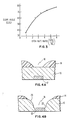
- FIG. 4A shows a portion of an insulating layer 10, for example, silicon dio xide which may be formed on a silicon body (not shown) or other underlying layer. Included in layer 10, for purposes of illustration, is a conductor 12 which may be a portion of a metallic interconnection layer. Overlying layer 10 is a mask layer 14, for example, a hydrocarbon photoresist, including mask openings 16 through which layer 10 will be etched. Mask opening 16 can be formed by any of a number of well known processes.
- Fig 4B shows layer 10 after the completion of the present etching process wherein an opening 18 has been formed.
- the upper sidewall portion 20 of opening 18 is formed by using an etchant having a high percentage CHF3 gas concentration during the initial phase of the etching process.
- the etchant has a high etch rate ratio of SiO2:HC and therefore causes sidewall portion 20 to initially have a high slope angle with respect to the horizontal.
- a smaller thickness of the photoresist layer 14 is etched as compared to the thickness of the SiO2 layer 10 etched during the initial etching phase.
- the percentage CHF3 gas concentration is decreased.
- the etch rate ratio is similarly decreased resulting in a high final slope angle for the lower sidewall portion 22 of opening 18 as compared to upper portion 20. That is, since a greater thickness of photoresist layer 14 is etched than during the initial etching phase, a larger surface area of SiO2 layer 10 will be uncovered during the final etching phase, causing the upper portion 20 of layer 10 to have a shallower final etched slope than the lower portion 22. In the example shown in Fig. 4B, the etching process is completed when the upper surface of conductor 12 is fully exposed.
- a silicon wafer having a 2.0 ⁇ m SiO2 layer thereon was etched through a 2000 nm diameter opening in a photoresist layer approximately 1500 nm thick.
- the process was carried out in a single wafer, planar plasma reactor at an RF frequency of about 13.56 MHz., an RF power of about 200 watts and a pressure of about 1.33 mbar.
- the initial CHF3 gas concentration was about 25%, and the final CHF3 gas concentration was about 5%, resulting in a lower sidewall slope of about 85 degrees and an upper sidewall slope of about 30 degrees.
- the entire etching process took approximately two minutes.
- This process is particularly adaptable to single wafer, high pressure plasma reactors having a relatively small plasma chamber volume, for example, less than about 40 ccm.
- the small chamber volume results in a low residence time and permits the precise control of the opening profile, since a change in CHF3 concentration causes an extremely fast change in the etch rate ratio. Under the above-described process conditions this change has been observed to occur in less than 0.5 seconds.
- the etchant gas concentration is changed abruptly during the etch cycle, a slight discontinuity in the etched profile is observed. Although this will not affect step coverage during subsequent metal deposition, the discontinuity can be avoided and the smoothly varying profile as shown in FIG. 4B can be achieved by continuously varying the CHF3 concentration. This can be readily carried out by using, for example, a microprocessor or an analog control loop.
Landscapes
- Engineering & Computer Science (AREA)
- Chemical & Material Sciences (AREA)
- Condensed Matter Physics & Semiconductors (AREA)
- Inorganic Chemistry (AREA)
- Physics & Mathematics (AREA)
- General Chemical & Material Sciences (AREA)
- Chemical Kinetics & Catalysis (AREA)
- General Physics & Mathematics (AREA)
- Manufacturing & Machinery (AREA)
- Computer Hardware Design (AREA)
- Microelectronics & Electronic Packaging (AREA)
- Power Engineering (AREA)
- Drying Of Semiconductors (AREA)
Applications Claiming Priority (2)
| Application Number | Priority Date | Filing Date | Title |
|---|---|---|---|
| US06/730,976 US4671849A (en) | 1985-05-06 | 1985-05-06 | Method for control of etch profile |
| US730976 | 1985-05-06 |
Publications (3)
| Publication Number | Publication Date |
|---|---|
| EP0201037A2 EP0201037A2 (en) | 1986-11-12 |
| EP0201037A3 EP0201037A3 (en) | 1988-03-23 |
| EP0201037B1 true EP0201037B1 (en) | 1991-06-26 |
Family
ID=24937562
Family Applications (1)
| Application Number | Title | Priority Date | Filing Date |
|---|---|---|---|
| EP86105947A Expired EP0201037B1 (en) | 1985-05-06 | 1986-04-30 | Method for etching openings with a controlled wall profile |
Country Status (5)
| Country | Link |
|---|---|
| US (1) | US4671849A (enExample) |
| EP (1) | EP0201037B1 (enExample) |
| JP (1) | JPS61256724A (enExample) |
| CA (1) | CA1261785A (enExample) |
| DE (1) | DE3679933D1 (enExample) |
Families Citing this family (46)
| Publication number | Priority date | Publication date | Assignee | Title |
|---|---|---|---|---|
| DE68922474T2 (de) * | 1988-12-09 | 1996-01-11 | Philips Electronics Nv | Verfahren zum Herstellen einer integrierten Schaltung einschliesslich Schritte zum Herstellen einer Verbindung zwischen zwei Schichten. |
| US5174857A (en) * | 1990-10-29 | 1992-12-29 | Gold Star Co., Ltd. | Slope etching process |
| US5317938A (en) * | 1992-01-16 | 1994-06-07 | Duke University | Method for making microstructural surgical instruments |
| US5880036A (en) * | 1992-06-15 | 1999-03-09 | Micron Technology, Inc. | Method for enhancing oxide to nitride selectivity through the use of independent heat control |
| US5651855A (en) * | 1992-07-28 | 1997-07-29 | Micron Technology, Inc. | Method of making self aligned contacts to silicon substrates during the manufacture of integrated circuits |
| JP2787646B2 (ja) | 1992-11-27 | 1998-08-20 | 三菱電機株式会社 | 半導体装置の製造方法 |
| US5466626A (en) * | 1993-12-16 | 1995-11-14 | International Business Machines Corporation | Micro mask comprising agglomerated material |
| US6870272B2 (en) * | 1994-09-20 | 2005-03-22 | Tessera, Inc. | Methods of making microelectronic assemblies including compliant interfaces |
| US5842387A (en) * | 1994-11-07 | 1998-12-01 | Marcus; Robert B. | Knife blades having ultra-sharp cutting edges and methods of fabrication |
| US6040247A (en) * | 1995-01-10 | 2000-03-21 | Lg Semicon Co., Ltd. | Method for etching contact |
| US6284563B1 (en) * | 1995-10-31 | 2001-09-04 | Tessera, Inc. | Method of making compliant microelectronic assemblies |
| US6211572B1 (en) * | 1995-10-31 | 2001-04-03 | Tessera, Inc. | Semiconductor chip package with fan-in leads |
| KR0179792B1 (ko) * | 1995-12-27 | 1999-04-15 | 문정환 | 고밀도 플라즈마 식각장비를 이용한 슬로프 콘택 홀 형성방법 |
| KR0179791B1 (ko) * | 1995-12-27 | 1999-03-20 | 문정환 | 플래쉬 메모리 소자 및 그 제조방법 |
| US6033991A (en) * | 1997-09-29 | 2000-03-07 | Cypress Semiconductor Corporation | Isolation scheme based on recessed locos using a sloped Si etch and dry field oxidation |
| US6074957A (en) * | 1998-02-26 | 2000-06-13 | Micron Technology, Inc. | Methods of forming openings and methods of controlling the degree of taper of openings |
| AU2002220595A1 (en) | 2000-10-11 | 2002-04-22 | Koninklijke Philips Electronics N.V. | Scalable coding of multi-media objects |
| US20050161429A1 (en) * | 2002-02-07 | 2005-07-28 | Andrew Sauciunac | Non-symmetrical photo tooling and dual surface etching |
| RU2314905C2 (ru) | 2002-03-11 | 2008-01-20 | Бектон, Дикинсон Энд Компани | Способ изготовления хирургических лезвий (варианты) |
| US7387742B2 (en) * | 2002-03-11 | 2008-06-17 | Becton, Dickinson And Company | Silicon blades for surgical and non-surgical use |
| US20040087153A1 (en) * | 2002-10-31 | 2004-05-06 | Yan Du | Method of etching a silicon-containing dielectric material |
| US7355687B2 (en) * | 2003-02-20 | 2008-04-08 | Hunter Engineering Company | Method and apparatus for vehicle service system with imaging components |
| JP2006518944A (ja) * | 2003-02-25 | 2006-08-17 | テッセラ,インコーポレイテッド | バンプを有するボールグリッドアレー |
| US20050155955A1 (en) * | 2003-03-10 | 2005-07-21 | Daskal Vadim M. | Method for reducing glare and creating matte finish of controlled density on a silicon surface |
| US20090007436A1 (en) * | 2003-03-10 | 2009-01-08 | Daskal Vadim M | Silicon blades for surgical and non-surgical use |
| JP2007514457A (ja) * | 2003-09-17 | 2007-06-07 | ベクトン・ディキンソン・アンド・カンパニー | シリコンおよびその他の結晶質材料にルータを用いて直線状および非直線状の溝を作成するシステムおよび方法 |
| US20050211171A1 (en) * | 2004-03-26 | 2005-09-29 | Applied Materials, Inc. | Chemical vapor deposition plasma reactor having an ion shower grid |
| US7244474B2 (en) * | 2004-03-26 | 2007-07-17 | Applied Materials, Inc. | Chemical vapor deposition plasma process using an ion shower grid |
| US7695590B2 (en) * | 2004-03-26 | 2010-04-13 | Applied Materials, Inc. | Chemical vapor deposition plasma reactor having plural ion shower grids |
| US20050211547A1 (en) * | 2004-03-26 | 2005-09-29 | Applied Materials, Inc. | Reactive sputter deposition plasma reactor and process using plural ion shower grids |
| US20050211546A1 (en) * | 2004-03-26 | 2005-09-29 | Applied Materials, Inc. | Reactive sputter deposition plasma process using an ion shower grid |
| US7291360B2 (en) * | 2004-03-26 | 2007-11-06 | Applied Materials, Inc. | Chemical vapor deposition plasma process using plural ion shower grids |
| US7396484B2 (en) * | 2004-04-30 | 2008-07-08 | Becton, Dickinson And Company | Methods of fabricating complex blade geometries from silicon wafers and strengthening blade geometries |
| US8058156B2 (en) * | 2004-07-20 | 2011-11-15 | Applied Materials, Inc. | Plasma immersion ion implantation reactor having multiple ion shower grids |
| US7767561B2 (en) * | 2004-07-20 | 2010-08-03 | Applied Materials, Inc. | Plasma immersion ion implantation reactor having an ion shower grid |
| JP4484641B2 (ja) * | 2004-09-10 | 2010-06-16 | Okiセミコンダクタ株式会社 | 強誘電体メモリの製造方法 |
| EP1851798B1 (en) * | 2005-02-25 | 2016-08-03 | Tessera, Inc. | Microelectronic assemblies having compliancy |
| US7883631B2 (en) * | 2006-03-07 | 2011-02-08 | Tokyo Electron Limited | Plasma etching method, plasma etching apparatus, control program and computer-readable storage medium |
| US7749886B2 (en) * | 2006-12-20 | 2010-07-06 | Tessera, Inc. | Microelectronic assemblies having compliancy and methods therefor |
| US8196285B1 (en) * | 2008-12-17 | 2012-06-12 | Western Digital (Fremont), Llc | Method and system for providing a pole for a perpendicular magnetic recording head using a multi-layer hard mask |
| US8254060B1 (en) | 2009-04-17 | 2012-08-28 | Western Digital (Fremont), Llc | Straight top main pole for PMR bevel writer |
| US8225488B1 (en) | 2009-05-22 | 2012-07-24 | Western Digital (Fremont), Llc | Method for providing a perpendicular magnetic recording (PMR) pole |
| US9346672B1 (en) | 2009-08-04 | 2016-05-24 | Western Digital (Fremont), Llc | Methods for fabricating damascene write poles using ruthenium hard masks |
| US8298881B2 (en) | 2010-06-28 | 2012-10-30 | International Business Machines Corporation | Nanowire FET with trapezoid gate structure |
| US8525338B2 (en) | 2011-06-07 | 2013-09-03 | Tessera, Inc. | Chip with sintered connections to package |
| EP2819162B1 (en) | 2013-06-24 | 2020-06-17 | IMEC vzw | Method for producing contact areas on a semiconductor substrate |
Family Cites Families (13)
| Publication number | Priority date | Publication date | Assignee | Title |
|---|---|---|---|---|
| GB1417085A (en) * | 1973-05-17 | 1975-12-10 | Standard Telephones Cables Ltd | Plasma etching |
| DE2658448C3 (de) * | 1976-12-23 | 1979-09-20 | Deutsche Itt Industries Gmbh, 7800 Freiburg | Verfahren zum Ätzen einer auf einem Halbleiterkörper aufgebrachten Schicht aus Siliciumnitrid in einem Gasplasma |
| US4283249A (en) * | 1979-05-02 | 1981-08-11 | International Business Machines Corporation | Reactive ion etching |
| US4324611A (en) * | 1980-06-26 | 1982-04-13 | Branson International Plasma Corporation | Process and gas mixture for etching silicon dioxide and silicon nitride |
| JPS57164529A (en) * | 1981-04-03 | 1982-10-09 | Oki Electric Ind Co Ltd | Dry etching method |
| US4409319A (en) * | 1981-07-15 | 1983-10-11 | International Business Machines Corporation | Electron beam exposed positive resist mask process |
| JPS58197820A (ja) * | 1982-05-14 | 1983-11-17 | Nippon Telegr & Teleph Corp <Ntt> | プラズマエツチング方法 |
| US4417947A (en) * | 1982-07-16 | 1983-11-29 | Signetics Corporation | Edge profile control during patterning of silicon by dry etching with CCl4 -O2 mixtures |
| DE3306703A1 (de) * | 1983-02-25 | 1984-08-30 | Siemens AG, 1000 Berlin und 8000 München | Verfahren zum herstellen von halbleitervorrichtungen |
| US4511430A (en) * | 1984-01-30 | 1985-04-16 | International Business Machines Corporation | Control of etch rate ratio of SiO2 /photoresist for quartz planarization etch back process |
| JPS60182136A (ja) * | 1984-02-29 | 1985-09-17 | Fujitsu Ltd | エツチング方法 |
| US4484979A (en) * | 1984-04-16 | 1984-11-27 | At&T Bell Laboratories | Two-step anisotropic etching process for patterning a layer without penetrating through an underlying thinner layer |
| JPS61114530A (ja) * | 1984-11-09 | 1986-06-02 | Oki Electric Ind Co Ltd | ドライエツチング方法及びその装置 |
-
1985
- 1985-05-06 US US06/730,976 patent/US4671849A/en not_active Expired - Lifetime
-
1986
- 1986-03-24 CA CA000504799A patent/CA1261785A/en not_active Expired
- 1986-04-04 JP JP61076856A patent/JPS61256724A/ja active Granted
- 1986-04-30 EP EP86105947A patent/EP0201037B1/en not_active Expired
- 1986-04-30 DE DE8686105947T patent/DE3679933D1/de not_active Expired - Lifetime
Also Published As
| Publication number | Publication date |
|---|---|
| EP0201037A2 (en) | 1986-11-12 |
| US4671849A (en) | 1987-06-09 |
| EP0201037A3 (en) | 1988-03-23 |
| CA1261785A (en) | 1989-09-26 |
| JPH0519977B2 (enExample) | 1993-03-18 |
| DE3679933D1 (de) | 1991-08-01 |
| JPS61256724A (ja) | 1986-11-14 |
Similar Documents
| Publication | Publication Date | Title |
|---|---|---|
| EP0201037B1 (en) | Method for etching openings with a controlled wall profile | |
| US7153779B2 (en) | Method to eliminate striations and surface roughness caused by dry etch | |
| EP0263220B1 (en) | Method of forming a via-having a desired slope in a photoresist masked composite insulating layer | |
| EP0243273B1 (en) | Method for planarizing semiconductor substrates | |
| US4522681A (en) | Method for tapered dry etching | |
| KR100778260B1 (ko) | 수소로 포토레지스트를 포스트 에칭 박리하기 위한 프로세스 | |
| US5691246A (en) | In situ etch process for insulating and conductive materials | |
| US20020052113A1 (en) | Two etchant etch method | |
| EP0436387A2 (en) | Single chamber via etch through a dual-layer dielectric | |
| WO2002065512A2 (en) | Process for etching organic low-k materials | |
| US6890863B1 (en) | Etchant and method of use | |
| WO2002065530A2 (en) | Use of hydrocarbon addition for the elimination of micromasking during etching of organic low-k dielectrics | |
| KR100743873B1 (ko) | 플라즈마 처리 챔버 내에서의 에칭을 개선하기 위한 기술 | |
| EP0536968A2 (en) | Process for forming contact holes in the fabrication of semi-conducteur devices | |
| US5167762A (en) | Anisotropic etch method | |
| KR100311487B1 (ko) | 산화막식각방법 | |
| JP2002520848A (ja) | 2ステップ自己整合コンタクトエッチング | |
| US4678540A (en) | Plasma etch process | |
| US20030190814A1 (en) | Method of reducing micromasking during plasma etching of a silicon-comprising substrate | |
| US5968278A (en) | High aspect ratio contact | |
| JPH02156529A (ja) | 半導体ウェーハの酸化物層傾斜エッチング方法 | |
| US20010006850A1 (en) | Method for manufacturing contact hole in semiconductor device | |
| JPH10177997A (ja) | Barcおよび窒化物のその場エッチングプロセス | |
| JPH06318576A (ja) | ドライエッチング方法 | |
| KR930008841B1 (ko) | 반도체 제조중 콘택트홀의 형성방법 |
Legal Events
| Date | Code | Title | Description |
|---|---|---|---|
| PUAI | Public reference made under article 153(3) epc to a published international application that has entered the european phase |
Free format text: ORIGINAL CODE: 0009012 |
|
| AK | Designated contracting states |
Kind code of ref document: A2 Designated state(s): DE FR GB IT |
|
| PUAB | Information related to the publication of an a document modified or deleted |
Free format text: ORIGINAL CODE: 0009199EPPU |
|
| RA1 | Application published (corrected) |
Date of ref document: 19861217 Kind code of ref document: A2 |
|
| 17P | Request for examination filed |
Effective date: 19870327 |
|
| PUAL | Search report despatched |
Free format text: ORIGINAL CODE: 0009013 |
|
| AK | Designated contracting states |
Kind code of ref document: A3 Designated state(s): DE FR GB IT |
|
| 17Q | First examination report despatched |
Effective date: 19900123 |
|
| GRAA | (expected) grant |
Free format text: ORIGINAL CODE: 0009210 |
|
| AK | Designated contracting states |
Kind code of ref document: B1 Designated state(s): DE FR GB IT |
|
| PG25 | Lapsed in a contracting state [announced via postgrant information from national office to epo] |
Ref country code: IT Free format text: LAPSE BECAUSE OF FAILURE TO SUBMIT A TRANSLATION OF THE DESCRIPTION OR TO PAY THE FEE WITHIN THE PRESCRIBED TIME-LIMIT;WARNING: LAPSES OF ITALIAN PATENTS WITH EFFECTIVE DATE BEFORE 2007 MAY HAVE OCCURRED AT ANY TIME BEFORE 2007. THE CORRECT EFFECTIVE DATE MAY BE DIFFERENT FROM THE ONE RECORDED. Effective date: 19910626 |
|
| REF | Corresponds to: |
Ref document number: 3679933 Country of ref document: DE Date of ref document: 19910801 |
|
| ET | Fr: translation filed | ||
| PLBE | No opposition filed within time limit |
Free format text: ORIGINAL CODE: 0009261 |
|
| STAA | Information on the status of an ep patent application or granted ep patent |
Free format text: STATUS: NO OPPOSITION FILED WITHIN TIME LIMIT |
|
| 26N | No opposition filed | ||
| PGFP | Annual fee paid to national office [announced via postgrant information from national office to epo] |
Ref country code: GB Payment date: 19970325 Year of fee payment: 12 |
|
| PGFP | Annual fee paid to national office [announced via postgrant information from national office to epo] |
Ref country code: FR Payment date: 19970401 Year of fee payment: 12 |
|
| PGFP | Annual fee paid to national office [announced via postgrant information from national office to epo] |
Ref country code: DE Payment date: 19970422 Year of fee payment: 12 |
|
| PG25 | Lapsed in a contracting state [announced via postgrant information from national office to epo] |
Ref country code: FR Free format text: THE PATENT HAS BEEN ANNULLED BY A DECISION OF A NATIONAL AUTHORITY Effective date: 19980430 Ref country code: GB Free format text: LAPSE BECAUSE OF NON-PAYMENT OF DUE FEES Effective date: 19980430 |
|
| GBPC | Gb: european patent ceased through non-payment of renewal fee |
Effective date: 19980430 |
|
| PG25 | Lapsed in a contracting state [announced via postgrant information from national office to epo] |
Ref country code: DE Free format text: LAPSE BECAUSE OF NON-PAYMENT OF DUE FEES Effective date: 19990202 |
|
| REG | Reference to a national code |
Ref country code: FR Ref legal event code: ST |