EP0198698A2 - Circuit intégré comportant une structure de ligne à ruban - Google Patents
Circuit intégré comportant une structure de ligne à ruban Download PDFInfo
- Publication number
- EP0198698A2 EP0198698A2 EP86302753A EP86302753A EP0198698A2 EP 0198698 A2 EP0198698 A2 EP 0198698A2 EP 86302753 A EP86302753 A EP 86302753A EP 86302753 A EP86302753 A EP 86302753A EP 0198698 A2 EP0198698 A2 EP 0198698A2
- Authority
- EP
- European Patent Office
- Prior art keywords
- strip line
- layer
- conductive layer
- microstrip line
- line structure
- Prior art date
- Legal status (The legal status is an assumption and is not a legal conclusion. Google has not performed a legal analysis and makes no representation as to the accuracy of the status listed.)
- Granted
Links
Images


Classifications
-
- H—ELECTRICITY
- H01—ELECTRIC ELEMENTS
- H01L—SEMICONDUCTOR DEVICES NOT COVERED BY CLASS H10
- H01L23/00—Details of semiconductor or other solid state devices
- H01L23/58—Structural electrical arrangements for semiconductor devices not otherwise provided for, e.g. in combination with batteries
- H01L23/64—Impedance arrangements
- H01L23/642—Capacitive arrangements
-
- H—ELECTRICITY
- H01—ELECTRIC ELEMENTS
- H01L—SEMICONDUCTOR DEVICES NOT COVERED BY CLASS H10
- H01L23/00—Details of semiconductor or other solid state devices
- H01L23/58—Structural electrical arrangements for semiconductor devices not otherwise provided for, e.g. in combination with batteries
- H01L23/64—Impedance arrangements
- H01L23/66—High-frequency adaptations
-
- H—ELECTRICITY
- H01—ELECTRIC ELEMENTS
- H01P—WAVEGUIDES; RESONATORS, LINES, OR OTHER DEVICES OF THE WAVEGUIDE TYPE
- H01P5/00—Coupling devices of the waveguide type
- H01P5/02—Coupling devices of the waveguide type with invariable factor of coupling
- H01P5/022—Transitions between lines of the same kind and shape, but with different dimensions
- H01P5/028—Transitions between lines of the same kind and shape, but with different dimensions between strip lines
-
- H—ELECTRICITY
- H01—ELECTRIC ELEMENTS
- H01P—WAVEGUIDES; RESONATORS, LINES, OR OTHER DEVICES OF THE WAVEGUIDE TYPE
- H01P5/00—Coupling devices of the waveguide type
- H01P5/08—Coupling devices of the waveguide type for linking dissimilar lines or devices
-
- H—ELECTRICITY
- H01—ELECTRIC ELEMENTS
- H01L—SEMICONDUCTOR DEVICES NOT COVERED BY CLASS H10
- H01L2223/00—Details relating to semiconductor or other solid state devices covered by the group H01L23/00
- H01L2223/58—Structural electrical arrangements for semiconductor devices not otherwise provided for
- H01L2223/64—Impedance arrangements
- H01L2223/66—High-frequency adaptations
- H01L2223/6605—High-frequency electrical connections
- H01L2223/6616—Vertical connections, e.g. vias
-
- H—ELECTRICITY
- H01—ELECTRIC ELEMENTS
- H01L—SEMICONDUCTOR DEVICES NOT COVERED BY CLASS H10
- H01L2224/00—Indexing scheme for arrangements for connecting or disconnecting semiconductor or solid-state bodies and methods related thereto as covered by H01L24/00
- H01L2224/01—Means for bonding being attached to, or being formed on, the surface to be connected, e.g. chip-to-package, die-attach, "first-level" interconnects; Manufacturing methods related thereto
- H01L2224/42—Wire connectors; Manufacturing methods related thereto
- H01L2224/47—Structure, shape, material or disposition of the wire connectors after the connecting process
- H01L2224/48—Structure, shape, material or disposition of the wire connectors after the connecting process of an individual wire connector
- H01L2224/4805—Shape
- H01L2224/4809—Loop shape
- H01L2224/48091—Arched
-
- H—ELECTRICITY
- H01—ELECTRIC ELEMENTS
- H01L—SEMICONDUCTOR DEVICES NOT COVERED BY CLASS H10
- H01L2224/00—Indexing scheme for arrangements for connecting or disconnecting semiconductor or solid-state bodies and methods related thereto as covered by H01L24/00
- H01L2224/01—Means for bonding being attached to, or being formed on, the surface to be connected, e.g. chip-to-package, die-attach, "first-level" interconnects; Manufacturing methods related thereto
- H01L2224/42—Wire connectors; Manufacturing methods related thereto
- H01L2224/47—Structure, shape, material or disposition of the wire connectors after the connecting process
- H01L2224/48—Structure, shape, material or disposition of the wire connectors after the connecting process of an individual wire connector
- H01L2224/481—Disposition
- H01L2224/48151—Connecting between a semiconductor or solid-state body and an item not being a semiconductor or solid-state body, e.g. chip-to-substrate, chip-to-passive
- H01L2224/48221—Connecting between a semiconductor or solid-state body and an item not being a semiconductor or solid-state body, e.g. chip-to-substrate, chip-to-passive the body and the item being stacked
- H01L2224/48225—Connecting between a semiconductor or solid-state body and an item not being a semiconductor or solid-state body, e.g. chip-to-substrate, chip-to-passive the body and the item being stacked the item being non-metallic, e.g. insulating substrate with or without metallisation
- H01L2224/48227—Connecting between a semiconductor or solid-state body and an item not being a semiconductor or solid-state body, e.g. chip-to-substrate, chip-to-passive the body and the item being stacked the item being non-metallic, e.g. insulating substrate with or without metallisation connecting the wire to a bond pad of the item
-
- H—ELECTRICITY
- H01—ELECTRIC ELEMENTS
- H01L—SEMICONDUCTOR DEVICES NOT COVERED BY CLASS H10
- H01L2224/00—Indexing scheme for arrangements for connecting or disconnecting semiconductor or solid-state bodies and methods related thereto as covered by H01L24/00
- H01L2224/01—Means for bonding being attached to, or being formed on, the surface to be connected, e.g. chip-to-package, die-attach, "first-level" interconnects; Manufacturing methods related thereto
- H01L2224/42—Wire connectors; Manufacturing methods related thereto
- H01L2224/47—Structure, shape, material or disposition of the wire connectors after the connecting process
- H01L2224/49—Structure, shape, material or disposition of the wire connectors after the connecting process of a plurality of wire connectors
- H01L2224/491—Disposition
- H01L2224/4912—Layout
- H01L2224/49171—Fan-out arrangements
-
- H—ELECTRICITY
- H01—ELECTRIC ELEMENTS
- H01L—SEMICONDUCTOR DEVICES NOT COVERED BY CLASS H10
- H01L24/00—Arrangements for connecting or disconnecting semiconductor or solid-state bodies; Methods or apparatus related thereto
- H01L24/01—Means for bonding being attached to, or being formed on, the surface to be connected, e.g. chip-to-package, die-attach, "first-level" interconnects; Manufacturing methods related thereto
- H01L24/42—Wire connectors; Manufacturing methods related thereto
- H01L24/47—Structure, shape, material or disposition of the wire connectors after the connecting process
- H01L24/48—Structure, shape, material or disposition of the wire connectors after the connecting process of an individual wire connector
-
- H—ELECTRICITY
- H01—ELECTRIC ELEMENTS
- H01L—SEMICONDUCTOR DEVICES NOT COVERED BY CLASS H10
- H01L24/00—Arrangements for connecting or disconnecting semiconductor or solid-state bodies; Methods or apparatus related thereto
- H01L24/01—Means for bonding being attached to, or being formed on, the surface to be connected, e.g. chip-to-package, die-attach, "first-level" interconnects; Manufacturing methods related thereto
- H01L24/42—Wire connectors; Manufacturing methods related thereto
- H01L24/47—Structure, shape, material or disposition of the wire connectors after the connecting process
- H01L24/49—Structure, shape, material or disposition of the wire connectors after the connecting process of a plurality of wire connectors
-
- H—ELECTRICITY
- H01—ELECTRIC ELEMENTS
- H01L—SEMICONDUCTOR DEVICES NOT COVERED BY CLASS H10
- H01L2924/00—Indexing scheme for arrangements or methods for connecting or disconnecting semiconductor or solid-state bodies as covered by H01L24/00
- H01L2924/0001—Technical content checked by a classifier
- H01L2924/00014—Technical content checked by a classifier the subject-matter covered by the group, the symbol of which is combined with the symbol of this group, being disclosed without further technical details
-
- H—ELECTRICITY
- H01—ELECTRIC ELEMENTS
- H01L—SEMICONDUCTOR DEVICES NOT COVERED BY CLASS H10
- H01L2924/00—Indexing scheme for arrangements or methods for connecting or disconnecting semiconductor or solid-state bodies as covered by H01L24/00
- H01L2924/01—Chemical elements
- H01L2924/01014—Silicon [Si]
-
- H—ELECTRICITY
- H01—ELECTRIC ELEMENTS
- H01L—SEMICONDUCTOR DEVICES NOT COVERED BY CLASS H10
- H01L2924/00—Indexing scheme for arrangements or methods for connecting or disconnecting semiconductor or solid-state bodies as covered by H01L24/00
- H01L2924/01—Chemical elements
- H01L2924/01039—Yttrium [Y]
-
- H—ELECTRICITY
- H01—ELECTRIC ELEMENTS
- H01L—SEMICONDUCTOR DEVICES NOT COVERED BY CLASS H10
- H01L2924/00—Indexing scheme for arrangements or methods for connecting or disconnecting semiconductor or solid-state bodies as covered by H01L24/00
- H01L2924/01—Chemical elements
- H01L2924/01057—Lanthanum [La]
-
- H—ELECTRICITY
- H01—ELECTRIC ELEMENTS
- H01L—SEMICONDUCTOR DEVICES NOT COVERED BY CLASS H10
- H01L2924/00—Indexing scheme for arrangements or methods for connecting or disconnecting semiconductor or solid-state bodies as covered by H01L24/00
- H01L2924/10—Details of semiconductor or other solid state devices to be connected
- H01L2924/11—Device type
- H01L2924/14—Integrated circuits
-
- H—ELECTRICITY
- H01—ELECTRIC ELEMENTS
- H01L—SEMICONDUCTOR DEVICES NOT COVERED BY CLASS H10
- H01L2924/00—Indexing scheme for arrangements or methods for connecting or disconnecting semiconductor or solid-state bodies as covered by H01L24/00
- H01L2924/15—Details of package parts other than the semiconductor or other solid state devices to be connected
- H01L2924/161—Cap
- H01L2924/1615—Shape
- H01L2924/16152—Cap comprising a cavity for hosting the device, e.g. U-shaped cap
-
- H—ELECTRICITY
- H01—ELECTRIC ELEMENTS
- H01L—SEMICONDUCTOR DEVICES NOT COVERED BY CLASS H10
- H01L2924/00—Indexing scheme for arrangements or methods for connecting or disconnecting semiconductor or solid-state bodies as covered by H01L24/00
- H01L2924/15—Details of package parts other than the semiconductor or other solid state devices to be connected
- H01L2924/161—Cap
- H01L2924/1615—Shape
- H01L2924/16195—Flat cap [not enclosing an internal cavity]
-
- H—ELECTRICITY
- H01—ELECTRIC ELEMENTS
- H01L—SEMICONDUCTOR DEVICES NOT COVERED BY CLASS H10
- H01L2924/00—Indexing scheme for arrangements or methods for connecting or disconnecting semiconductor or solid-state bodies as covered by H01L24/00
- H01L2924/19—Details of hybrid assemblies other than the semiconductor or other solid state devices to be connected
- H01L2924/1901—Structure
- H01L2924/1904—Component type
- H01L2924/19041—Component type being a capacitor
-
- H—ELECTRICITY
- H01—ELECTRIC ELEMENTS
- H01L—SEMICONDUCTOR DEVICES NOT COVERED BY CLASS H10
- H01L2924/00—Indexing scheme for arrangements or methods for connecting or disconnecting semiconductor or solid-state bodies as covered by H01L24/00
- H01L2924/30—Technical effects
- H01L2924/301—Electrical effects
- H01L2924/30107—Inductance
-
- H—ELECTRICITY
- H01—ELECTRIC ELEMENTS
- H01L—SEMICONDUCTOR DEVICES NOT COVERED BY CLASS H10
- H01L2924/00—Indexing scheme for arrangements or methods for connecting or disconnecting semiconductor or solid-state bodies as covered by H01L24/00
- H01L2924/30—Technical effects
- H01L2924/301—Electrical effects
- H01L2924/3011—Impedance
-
- H—ELECTRICITY
- H01—ELECTRIC ELEMENTS
- H01L—SEMICONDUCTOR DEVICES NOT COVERED BY CLASS H10
- H01L2924/00—Indexing scheme for arrangements or methods for connecting or disconnecting semiconductor or solid-state bodies as covered by H01L24/00
- H01L2924/30—Technical effects
- H01L2924/301—Electrical effects
- H01L2924/3025—Electromagnetic shielding
-
- H—ELECTRICITY
- H05—ELECTRIC TECHNIQUES NOT OTHERWISE PROVIDED FOR
- H05K—PRINTED CIRCUITS; CASINGS OR CONSTRUCTIONAL DETAILS OF ELECTRIC APPARATUS; MANUFACTURE OF ASSEMBLAGES OF ELECTRICAL COMPONENTS
- H05K1/00—Printed circuits
- H05K1/02—Details
- H05K1/0213—Electrical arrangements not otherwise provided for
- H05K1/0237—High frequency adaptations
-
- H—ELECTRICITY
- H05—ELECTRIC TECHNIQUES NOT OTHERWISE PROVIDED FOR
- H05K—PRINTED CIRCUITS; CASINGS OR CONSTRUCTIONAL DETAILS OF ELECTRIC APPARATUS; MANUFACTURE OF ASSEMBLAGES OF ELECTRICAL COMPONENTS
- H05K3/00—Apparatus or processes for manufacturing printed circuits
- H05K3/30—Assembling printed circuits with electric components, e.g. with resistor
- H05K3/32—Assembling printed circuits with electric components, e.g. with resistor electrically connecting electric components or wires to printed circuits
- H05K3/325—Assembling printed circuits with electric components, e.g. with resistor electrically connecting electric components or wires to printed circuits by abutting or pinching, i.e. without alloying process; mechanical auxiliary parts therefor
Definitions
- the present invention relates to an integrated circuit device. More particularly, it relates to an integrated circuit device suitably applicable to a high speed operation circuit and including a stacked layer unit having a triplate strip line structure therein.
- IC semiconductor integrated circuit
- Si silicon
- GaAs gallium-arsenic
- Such semiconductor IC chips must be naturally hermetically sealed by a package in the same way as for normal semiconductor IC chips.
- connection (lead) wires of resistive material between circuit elements in the device must be regarded as not only resistance components but also as inductance components, due to the application of a high frequency, and wires having a low resistance and low inductance are required for high speed signal transfer lines.
- wires having a high inductance are required for power supply lines and low speed signal transfer lines, to improve isolation between difference power sources and between the circuit elements in the device.
- an impedance matching of the connection wires is also required, thus a normal wire connection technology as used in well known normal semiconductor IC devices cannot be used.
- the high speed IC devices are provided with multi-stacked layers, each consisting of an insulation layer and a plurality of conductive layer strips, and connection members embedded in the multi-stacked layers in a direction perpendicular to the planes of the stacked layers.
- the IC chip in which the circuit elements are formed is mounted on the top of the stacked layers and hermetically sealed by the package.
- the connection of the circuit elements in the IC device is achieved by the connection members and the conductive layer strips of the multi-stacked layers.
- triplate strip lines or microstrip lines are used for such external connection wires.
- the triplate strip lines or microstrip lines suffer from the disadvantage of a poor impedance matching, etc., which will be described later with reference to a specific example.
- the above poor impedance matching is not admissible for high speed IC devices, e.g., approximately more than one giga bits per second.
- an integrated circuit device including: at least one semiconductor chip having a plurality of circuit elements; a package enclosing the semiconductor chip with a hermetic seal; and a strip line unit for connecting the circuit elements in the semiconductor chip to circuits outside of the package, having a microstrip line structure and a triplate strip line structure serial-connected to the microstrip line structure and connecting the outside circuits.
- the triplate strip line structure has a characteristic impedance equal to that of the microstrip line structure, so that the strip line unit has a satisfactory impedance matching.
- the strip line unit may be formed in a stacked layer unit including at least three stacked layers, each having an insulation layer and at least one conductive layer formed on a surface of the insulation layer, and a cavity defined by the package.
- a microstrip line of the microstrip line structure is connected to a center conductive layer strip line of the triplate strip line structure in series.
- the center conductive layer strip line has a predetermined impedance so that the triplate strip line structure has a same characteristic impedance as the microstrip line structure.
- the microstrip line structure may be formed by the microstrip line having predetermined thickness and width and facing the cavity, an insulation layer of the stacked layer unit having a predetermined dielectric constant and the microstrip line being mounted thereon at a plane, and a conductive layer of the stacked layer unit mounted on the insulation layer at another plane opposite to the plane of the microstrip line.
- the triplate strip line structure also may be formed by the center conductive layer strip line directly connected to the microstrip line, the insulation layer, the center conductive layer strip line mounted thereon at one plane, the conductive layer mounted on the insulation layer at another plane, another insulation layer having a predetermined dielectric constant and a predetermined length, formed on the center conductive layer strip line and the insulation layer and forming a part of the package, and another conductive layer formed on another insulation layer.
- the microstrip line and the center conductive layer strip line have the same thickness, and the center conductive layer strip line has a smaller width than that of the microstrip line along the length of the another insulation layer.
- the triplate strip line structure may be further formed by the center conductive layer strip line, a second insulation layer of the stacked layer unit having a predetermined dielectric constant, the conductive layer strip line contacting thereon at one plane, a second conductive layer formed on the second insulation layer at another plane, a third insulation layer of the stacked layer unit having a predetermined dielectric constant, the conductive layer strip line mounted thereon at one plane, and a third conductive layer formed on the third insulation layer at another plane.
- the microstrip line may be formed on a different insulation layer on which the center conductive layer strip line is formed. The microstrip line is connected to the center conductive layer strip line through a conductive member embedded in the second and third insulation layers in a direction perpendicular to a plane of the second and third insulation layers.
- the first conductive layer of the microstrip line structure and the second conductive layer of the triplate strip line structure may be unified and positioned on a same level in the stacked layer unit.
- the microstrip line and the center conductive layer strip line have same thickness, and the center conductive layer strip line has a smaller width than that of the microstrip line.
- the stacked layer unit may be formed as a part of the package.
- the semiconductor chip is mounted on a top insulation layer of the stacked layer unit.
- the semiconductor chip and the strip line unit are enclosed by the package and the stacked layer unit with a hermetic seal.
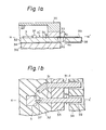
- an IC device includes a semiconductor IC chip 3 having a semiconductor substrate of Si or GaAs and a plurality of transistors and other circuit elements formed on the substrate and mounted on an insulation layer 32 of ceramic or the like.
- the IC device also includes a stacked layer structure consisting of a conductive wire strip 31 formed on the insulation layer 32, a metal film 34 placed beneath the insulation layer 32 and mounted on another insulation layer 36.
- the IC device further includes a package including an insulator 33 and a metal cap 35.
- a cavity. 20' wherein the IC chip 3 is located is defined and hermetically sealed by the package and the stacked layer structure.
- the conductive wire strip 31 is connected to a terminal of the IC chip 3 by soldering 31.
- the conductive wire strip 31 extends outside of the IC device through a hermetic seal portion and is soldered to a connection wire 39 on a substrate 38 positioned outside and adjacent to the IC device. Accordingly, the conductive wire strip 31 functions as an external connection wire.
- Another conductive wire strip 31-1 (Fig. lb) also can be provided.
- a structure of the conductive wire strip 31 indicated by reference Ai may be a microstrip line structure, because the metal film 34 is provided beneath the conductive wire strip 31 through the insulation layer 32, and the cavity 20' is provided above the conductive wire strip 31.
- another structure of the conductive wire strip 31 indicated by reference A 2 ' may be a balanced-type strip line structure, i.e. a triplate strip line structure, because the conductive wire strip 31 is provided between the metal cap 35 and the metal film 34 through the insulator 33 and the insulation layer 32, both having the same thickness and same dielectric constant.
- the thickness t 0 and width W 0 of the conductive wire strip 31 are identical at portions indicated by references Ai and A2.
- a characteristic impedance Z 0 at the portion indicated by reference Ai is 50 ⁇ , which is a desired characteristic impedance in the example.
- another characteristic impedance Z 0 ' at the portion indicated by reference A 2 ' will be reduced due to the effect of the dielectric constant of the insulator 33 and is approximately 33 ⁇ . As a result, a mismatching between the characteristic impedance brings about a reflection loss.
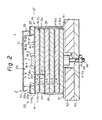
- an IC device 1 embodying the present invention includes a package 2 consisting of a cap 21 formed of an insulation material, an upper shield wall 22 formed of an insulation material, a seal layer 23 and a side wall 24 formed of an insulation material, an IC chip 3 including a plurality of circuit elements formed on a semiconductor substrate of Si or GaAs, and a stacked layer unit 11.
- the IC chip 3 is mounted on the top of the stacked layer unit 11 and is located in a hermetically sealed cavity 20 defined by the package 2 and the stacked layer unit 11.
- the above insulation material is a dielectric material.
- the IC device 1 is mounted on a printed circuit board 52 through conductive leads 51 and secured to a plate 53 through a stud 54 having one end fixed to a bottom surface 11-6C of the stacked layer unit 11, the shaft of the stud 54 passing through a hole 56 in the printed circuit board 52 and the plate 53, and the other end of the stud 54 being fastened thereto by a nut 55.
- the stacked layer unit 11 includes six stacked layers 11-1 to 11-6.
- Each of the stacked layers 11-1 to 11-6 includes an insulation layer or a dielectric layer as shown by the layer 11-lb for the upper layer 11-1, and at least one conductive layer strip as shown by the strip 11-la.
- the insulation layers 11-lb, etc. are formed of a sintered ceramic and have a thickness of approximately 330 ⁇ m and a dielectric constant of 10.
- Two conductive wire strips 15-1 and 15-2 are also provided on the insulation layer 11-lb adjacent to the IC chip 3.
- the conductive layer strips of the second layer 11-2 are used for ground lines or power supply lines.
- the conductive layer strips of the fourth and sixth layers 11-4 and 11-6 are also used for ground lines or power supply lines.
- Conductive layer strips of the third layer 11-3 are used for high speed signal lines.
- the conductive layer strips of the fifth layer 11-5 are used for low speed signal lines.
- Connection wires connecting between the circuit elements in the IC chip 3 are formed by the conductive layer strips and connection members embedded in the insulation layers in a direction perpendicular to the plane of the insulation layers and connecting between the circuit elements and the conductive layer strips. However, these internal connection wires are omitted in Fig. 2, because they do not directly pertain to the present invention.
- Figure 3a is a plan view of a part of the IC device in Fig. 2, indicated by references A 1 and A 2 in Fig. 2 and taken along the line H-H' in Fig. 2.
- Figure 3b is a sectional view of the IC device, taken along the line Y-Y' in Fig. 3a.
- Figures 3a and 3b correspond to Figs. la and lb discussed above.
- the conductive wire strip 15-2 includes a wide width portion 15-2a, a narrow width portion 15-2b, and a wide width portion 15-2c.
- the width W a of the wide width portions 15-2a and 15-2c is 300 ⁇ m and the width W b of the narrow width portion 15-2b is 100 ⁇ m.
- the thickness t of the conductive wire strip 15-2b is 15 ⁇ m, throughout the portions 15-2a to 15-2c.
- the length of the narrow width portion 15-2b is identical to that of the seal layer 23.
- the conductive wire strip 15-2 functions as an external connection wire.
- One end of the conductive wire strip 15-2 is connected to a terminal of the IC chip 3 at the wide width portion 15-2a inside of the IC device through a wire 18-2 and another end of the conductive wire strip 15-2 may be connected to other circuits in other IC devices by the wide width portion 15-2c outside of the IC device and extending on the side wall 24.
- the wide width portion 15-2C may be formed as a coplaner.
- the structure of the wide width portion 15-2a of the conductive wire strip 15-2 indicated by reference A in Fig. 2 is similar to that shown in Fig. la and thus is formed as a microstrip line structure, because the conductive layer 11-2a formed on the insulation layer 11-2b of the second layer 11-2 is provided beneath the wide width portion 15-2a and the cavity 20 is provided above the wide width portion 15-2a.
- the insulation layer 11-2b between the wide width portion 15-2a of the conductive wire strip 15-2 and the conductive layer 11-2a is also formed of a sintered ceramic and has a thickness of approximately 330 um and a dielectric constant of 10. As a result, a characteristic impedance of the microstrip line structure is 50 n.
- another structure of the conductive wire strip 15-2 indicated by reference A 2 includes the seal layer 23 consisting of an insulation layer 23b formed of a sintered ceramic and having a thickness t 23 of approximately 330 ⁇ m, identical to the thickness t 11-1 of the insulation layer 11-lb, and a dielectric constant of 10, and a conductive layer 23a formed on the insulation layer 23b, a narrow width portion 15-2b having the width Wb of 100 ⁇ m which is narrower than that of the wide width portion 15-2a, and the conductive layer 11-2a.
- Capacitors are formed in the insulation layer 23b and the insulation layer 11-lb. Accordingly, another structure is formed as a triplate strip line structure.
- the width W b of the narrow width portion 15-2b may be reduced.
- a characteristic impedance of the triplate strip line structure is 50 ⁇ , identical to that of the microstrip line structure set forth above.
- the impedance matching is achieved throughout the conductive wire strip 15-2 as the external connection wire, with the result that losses such as reflection loss do not occurs
- the essence is to make the characteristic impedance of the triplate strip line structure, which is affected by the insulation layer 23b, equal to that of the microstrip line structure. More specifically, a capacitance of the narrow width portion 15-2b is designed to have a predetermined impedance so that an impedance matching is achieved there between.
- the characteristic impedance can be arbitrary, such as 75 ⁇ .
- Figure 4 is a perspective view of the IC device at the portion indicated by reference B in Fig. 2.
- the conductive wire strip 15-1 formed on the insulation layer 11-lb is connected to the conductive strip 11-3a formed on the insulation layer 11-3b, through a viahole 14-1 which formed by charging an electrical conductive material in a throughhole 12-1 formed in a direction perpendicular to the plane of the stacked layer unit 11 and in the insulation layers 11-lb and 11-2b, and accordingly, becomes electrically conductive.
- a structure formation stack by the conductive layer 11-2a, the insulation layer 11-lb, the conductive wire strip 15-1, and the cavity 20 above the conductive wire strip 15-1 is formed as a microstrip line structure in the same way as set forth with reference to Figs. 3a and 3b.
- the thickness t l of the conductive wire strip 15-1 is 15 ⁇ m and the width W 1 300 ⁇ m, these being equal to those of the conductive wire strip 15-2.
- the thickness and material of the insulation layer 11-lb are as mentioned above. Accordingly, a characteristic impedance of the structure of the conductive wire strip 15-1 is 50 ⁇ .
- Another structure formed as a stack by the conductive layer 11-4a formed on the insulation layer 11-4b, the insulation layer ll-3b, the conductive strip 11-3a, the insulation layer 11-2b, and the conductive layer 11-2a is formed as a triplate strip line structure in the same way as set forth with reference to Figs. 3a and 3b.
- Capacitors CS 1 and CS 2 are formed in the insulation layers 11-2b and 11-3b.
- the thickness t 2 of the conductive strip 11-3a is identical to that of t 1 of the conductive wire strip 15-2, and the width W 2 of 100 ⁇ m is identical to that of W b in Fig. 3a.
- the width W 2 may be reduced as described previously.
- the thickness and material of the insulation layer 11-3b are identical to those of the insulation layer 11-2b.
- the width W 2 is smaller than the width W 1 , and accordingly, the triplate strip line structure has a characteristic impedance of 50 ⁇ identical to that of the microstrip line structure of the conductive wire strip 15-1, even if the affect of the dielectric constant of the insulation layer 11-2b is felt, as described above with reference to Figs. 3a and 3b.
- the impedance matching between the microstrip line structure and the triplate strip line structure is achieved throughout a connection line of the conductive wire strip 15-1, the viahole 14-1, and the conductive layer 11-3a, as an external connection wire, with the result that losses such as reflection loss do not occur.
- An end of the external connection wire is connected to a terminal of the IC chip 3 inside of the IC device, and another end outside of the IC device is connected to a coplaner 25 mounted on the surface of the side wall 24 as shown in Fig. 2.
Landscapes
- Power Engineering (AREA)
- Physics & Mathematics (AREA)
- General Physics & Mathematics (AREA)
- Engineering & Computer Science (AREA)
- Computer Hardware Design (AREA)
- Microelectronics & Electronic Packaging (AREA)
- Condensed Matter Physics & Semiconductors (AREA)
- Microwave Amplifiers (AREA)
- Waveguides (AREA)
- Inductance-Capacitance Distribution Constants And Capacitance-Resistance Oscillators (AREA)
- Coils Or Transformers For Communication (AREA)
- Internal Circuitry In Semiconductor Integrated Circuit Devices (AREA)
- Lead Frames For Integrated Circuits (AREA)
- Wire Bonding (AREA)
- Train Traffic Observation, Control, And Security (AREA)
Priority Applications (1)
| Application Number | Priority Date | Filing Date | Title |
|---|---|---|---|
| AT86302753T ATE68915T1 (de) | 1985-04-13 | 1986-04-14 | Integrierte schaltung mit eingebauter streifenleiterstruktur. |
Applications Claiming Priority (2)
| Application Number | Priority Date | Filing Date | Title |
|---|---|---|---|
| JP60077550A JPH0812887B2 (ja) | 1985-04-13 | 1985-04-13 | 高速集積回路パツケ−ジ |
| JP77550/85 | 1985-04-13 |
Publications (3)
| Publication Number | Publication Date |
|---|---|
| EP0198698A2 true EP0198698A2 (fr) | 1986-10-22 |
| EP0198698A3 EP0198698A3 (en) | 1988-08-03 |
| EP0198698B1 EP0198698B1 (fr) | 1991-10-23 |
Family
ID=13637119
Family Applications (1)
| Application Number | Title | Priority Date | Filing Date |
|---|---|---|---|
| EP86302753A Expired - Lifetime EP0198698B1 (fr) | 1985-04-13 | 1986-04-14 | Circuit intégré comportant une structure de ligne à ruban |
Country Status (8)
| Country | Link |
|---|---|
| US (1) | US4875087A (fr) |
| EP (1) | EP0198698B1 (fr) |
| JP (1) | JPH0812887B2 (fr) |
| AT (1) | ATE68915T1 (fr) |
| CA (1) | CA1246170A (fr) |
| DE (1) | DE3682101D1 (fr) |
| HK (1) | HK56592A (fr) |
| SG (1) | SG58992G (fr) |
Cited By (20)
| Publication number | Priority date | Publication date | Assignee | Title |
|---|---|---|---|---|
| EP0283396A1 (fr) * | 1987-03-20 | 1988-09-21 | Thomson-Csf | Jonction entre une ligne triplaque et une ligne microruban, et applications |
| FR2630261A1 (fr) * | 1988-04-15 | 1989-10-20 | Trt Telecom Radio Electr | Circuit utilisable dans le domaine des hyperfrequences |
| US4949163A (en) * | 1987-04-15 | 1990-08-14 | Kabushiki Kaisha Toshiba | Semiconductor integrated circuit device particularly for high speed logic operations |
| US5021866A (en) * | 1987-09-28 | 1991-06-04 | Kabushiki Kaisha Toshiba | Semiconductor integrated circuit apparatus |
| EP0436848A2 (fr) * | 1990-01-10 | 1991-07-17 | International Business Machines Corporation | Conducteurs verticaux à impédance adaptée dans un substrat laminaire métal-diélectrique à multi-couches |
| GB2247786A (en) * | 1990-09-04 | 1992-03-11 | Watkins Johnson Co | Microwave modules and connecting system therefor |
| EP0478160A2 (fr) * | 1990-09-28 | 1992-04-01 | Fujitsu Limited | Boîtier de circuit intégré comportant des conducteurs électriques dans un corps diélectrique d'emballage |
| US5136271A (en) * | 1989-01-09 | 1992-08-04 | Mitsubishi Denki Kabushiki Kaisha | Microwave integrated circuit mountings |
| US5157477A (en) * | 1990-01-10 | 1992-10-20 | International Business Machines Corporation | Matched impedance vertical conductors in multilevel dielectric laminated wiring |
| EP0525810A1 (fr) * | 1991-07-31 | 1993-02-03 | Hughes Aircraft Company | Transition avec impédance constante entre structures de transmission de dimensions diverses |
| EP0563873A2 (fr) * | 1992-04-03 | 1993-10-06 | Matsushita Electric Industrial Co., Ltd. | Substrat céramique à multi-couche pour hautes fréquences |
| FR2695514A1 (fr) * | 1992-09-10 | 1994-03-11 | Alcatel Telspace | Dispositif hyperfréquence comprenant un filtre triplaque réalisé dans une semelle conductrice d'électricité recouverte d'un matériau diélectrique. |
| EP0617466A2 (fr) * | 1993-03-24 | 1994-09-28 | Intergraph Corporation | Empaquetage multi-couche amélioré |
| DE19534309C1 (de) * | 1995-09-15 | 1997-03-27 | Siemens Ag | Anordnung zum Übertragen von Signalen über Triplate-Leitungen |
| FR2739496A1 (fr) * | 1995-10-03 | 1997-04-04 | Dassault Electronique | Circuit hyperfrequence multicouches a elements actifs integres |
| FR2739492A1 (fr) * | 1995-10-03 | 1997-04-04 | Dassault Electronique | Circuit hyperfrequence multi-couches a elements actifs integres |
| EP0795907A1 (fr) * | 1996-03-14 | 1997-09-17 | Dassault Electronique | Circuit hyperfréquence multicouches à éléments actifs intégrés |
| US6225696B1 (en) * | 1997-09-18 | 2001-05-01 | Trw Inc. | Advanced RF electronics package |
| EP1202377A2 (fr) * | 2000-10-31 | 2002-05-02 | Mitsubishi Denki Kabushiki Kaisha | Dispositif multicouche à transitions verticales pour lignes à bandes et module optique |
| EP1293009A1 (fr) * | 2000-06-09 | 2003-03-19 | Synergy Microwave Corproation | Circuits hyperfrequences multicouches et leurs procedes de fabrication |
Families Citing this family (36)
| Publication number | Priority date | Publication date | Assignee | Title |
|---|---|---|---|---|
| JP2580674B2 (ja) * | 1988-02-08 | 1997-02-12 | 三菱電機株式会社 | 高周波用モールド型パッケージ |
| US5065227A (en) * | 1990-06-04 | 1991-11-12 | International Business Machines Corporation | Integrated circuit packaging using flexible substrate |
| CA2047486C (fr) * | 1990-07-21 | 2002-03-05 | Shigeru Katayama | Dispositif a semi-conducteur et methode de fabrication de ce dispositif |
| US5132613A (en) * | 1990-11-30 | 1992-07-21 | International Business Machines Corporation | Low inductance side mount decoupling test structure |
| US5376909A (en) * | 1992-05-29 | 1994-12-27 | Texas Instruments Incorporated | Device packaging |
| US6271579B1 (en) * | 1993-10-08 | 2001-08-07 | Stratedge Corporation | High-frequency passband microelectronics package |
| JPH10501102A (ja) * | 1995-03-02 | 1998-01-27 | サーキット コンポーネンツ インコーポレーテッド | Bga i/o rfポートフォーマットとセラミックス基板技術とを使用した90ghzまでの周波数領域のマイクロ波回路用の低コスト高性能パッケージ |
| GB2298957A (en) * | 1995-03-16 | 1996-09-18 | Oxley Dev Co Ltd | Microstrip microwave package |
| US5952709A (en) * | 1995-12-28 | 1999-09-14 | Kyocera Corporation | High-frequency semiconductor device and mounted structure thereof |
| US6018283A (en) * | 1996-12-18 | 2000-01-25 | Texas Instruments Incorporated | Ultrawide bandwidth Z-axis interconnect |
| US6687842B1 (en) * | 1997-04-02 | 2004-02-03 | Tessera, Inc. | Off-chip signal routing between multiply-connected on-chip electronic elements via external multiconductor transmission line on a dielectric element |
| US9054094B2 (en) | 1997-04-08 | 2015-06-09 | X2Y Attenuators, Llc | Energy conditioning circuit arrangement for integrated circuit |
| US7336468B2 (en) | 1997-04-08 | 2008-02-26 | X2Y Attenuators, Llc | Arrangement for energy conditioning |
| US7321485B2 (en) | 1997-04-08 | 2008-01-22 | X2Y Attenuators, Llc | Arrangement for energy conditioning |
| US5923234A (en) * | 1997-10-27 | 1999-07-13 | Lockheed Martin Corp. | Hermetic feedthrough using three-via transmission lines |
| US6057600A (en) * | 1997-11-27 | 2000-05-02 | Kyocera Corporation | Structure for mounting a high-frequency package |
| KR100563122B1 (ko) * | 1998-01-30 | 2006-03-21 | 다이요 유덴 가부시키가이샤 | 하이브리드 모듈 및 그 제조방법 및 그 설치방법 |
| US6225690B1 (en) * | 1999-12-10 | 2001-05-01 | Lsi Logic Corporation | Plastic ball grid array package with strip line configuration |
| JP2001308547A (ja) * | 2000-04-27 | 2001-11-02 | Sharp Corp | 高周波多層回路基板 |
| TW452953B (en) * | 2000-05-22 | 2001-09-01 | Via Tech Inc | BGA chip package capable of decreasing its impedance when operating at high frequency |
| JP4462758B2 (ja) * | 2000-12-27 | 2010-05-12 | 京セラ株式会社 | 高周波用配線基板 |
| FR2826780A1 (fr) * | 2001-06-28 | 2003-01-03 | St Microelectronics Sa | Dispositif semi-conducteur a structure hyperfrequence |
| DE10212769A1 (de) * | 2002-03-22 | 2003-10-02 | Dystar Textilfarben Gmbh & Co | Farbstoffmischungen von faserreaktiven Azofarbstoffen, ihre Herstellung und ihre Verwendung |
| JP2005086603A (ja) * | 2003-09-10 | 2005-03-31 | Tdk Corp | 電子部品モジュールおよびその製造方法 |
| JP2008537843A (ja) | 2005-03-01 | 2008-09-25 | エックストゥーワイ アテニュエイターズ,エルエルシー | 内部で重なり合った調整器 |
| US8159832B2 (en) * | 2007-09-21 | 2012-04-17 | Nokia Corporation | Electromagnetic band gap structures and method for making same |
| US8081045B1 (en) * | 2008-08-08 | 2011-12-20 | Lockheed Martin Corporation | Beamformer power divider/combiner with transmission lines distributed between MMIC and associated PC board |
| JP5636834B2 (ja) * | 2010-09-10 | 2014-12-10 | 富士通株式会社 | 高周波回路用パッケージ及び高周波回路装置 |
| US10062972B1 (en) * | 2013-04-23 | 2018-08-28 | National Technology & Engineering Solutions Of Sandia, Llc | Antenna array with low Rx and Tx sidelobe levels |
| JP7155261B2 (ja) | 2017-11-10 | 2022-10-18 | レイセオン カンパニー | 無線周波数回路におけるアディティブ製造技術(amt)ファラデー境界 |
| US20190150296A1 (en) * | 2017-11-10 | 2019-05-16 | Raytheon Company | Additive manufacturing technology microwave vertical launch |
| US11289814B2 (en) | 2017-11-10 | 2022-03-29 | Raytheon Company | Spiral antenna and related fabrication techniques |
| EP4235951A3 (fr) | 2017-11-10 | 2023-09-06 | Raytheon Company | Radiateur à profil bas de technologie de fabrication additive (amt) |
| KR102342520B1 (ko) | 2017-11-10 | 2021-12-22 | 레이던 컴퍼니 | 밀리미터파 전송 라인 구조 |
| EP3760014B1 (fr) | 2018-02-28 | 2022-09-28 | Raytheon Company | Interconnexions rf rapides |
| US11089687B2 (en) | 2018-02-28 | 2021-08-10 | Raytheon Company | Additive manufacturing technology (AMT) low profile signal divider |
Citations (4)
| Publication number | Priority date | Publication date | Assignee | Title |
|---|---|---|---|---|
| US4047132A (en) * | 1975-06-20 | 1977-09-06 | International Computers Limited | Multilayer printed circuit boards |
| GB2007911A (en) * | 1977-10-12 | 1979-05-23 | Secr Defence | Microwave device package |
| EP0198621A2 (fr) * | 1985-03-30 | 1986-10-22 | Fujitsu Limited | Dispositif semi-conducteur |
| GB2181300A (en) * | 1985-09-26 | 1987-04-15 | Int Standard Electric Corp | Semiconductor chip housing and method of manufacture |
Family Cites Families (5)
| Publication number | Priority date | Publication date | Assignee | Title |
|---|---|---|---|---|
| US3715635A (en) * | 1971-06-25 | 1973-02-06 | Bendix Corp | High frequency matched impedance microcircuit holder |
| US4259684A (en) * | 1978-10-13 | 1981-03-31 | The Secretary Of State For Defence In Her Britannic Majesty's Government Of The United Kingdom Of Great Britain And Northern Ireland | Packages for microwave integrated circuits |
| US4276558A (en) * | 1979-06-15 | 1981-06-30 | Ford Aerospace & Communications Corp. | Hermetically sealed active microwave integrated circuit |
| GB2078845A (en) * | 1980-06-23 | 1982-01-13 | Electronic Locks Sweden Ab | Lock system for storage units |
| US4498122A (en) * | 1982-12-29 | 1985-02-05 | At&T Bell Laboratories | High-speed, high pin-out LSI chip package |
-
1985
- 1985-04-13 JP JP60077550A patent/JPH0812887B2/ja not_active Expired - Lifetime
-
1986
- 1986-04-09 CA CA000506182A patent/CA1246170A/fr not_active Expired
- 1986-04-14 EP EP86302753A patent/EP0198698B1/fr not_active Expired - Lifetime
- 1986-04-14 DE DE8686302753T patent/DE3682101D1/de not_active Expired - Fee Related
- 1986-04-14 AT AT86302753T patent/ATE68915T1/de not_active IP Right Cessation
-
1988
- 1988-07-22 US US07/222,303 patent/US4875087A/en not_active Expired - Fee Related
-
1992
- 1992-06-03 SG SG589/92A patent/SG58992G/en unknown
- 1992-07-30 HK HK565/92A patent/HK56592A/xx unknown
Patent Citations (4)
| Publication number | Priority date | Publication date | Assignee | Title |
|---|---|---|---|---|
| US4047132A (en) * | 1975-06-20 | 1977-09-06 | International Computers Limited | Multilayer printed circuit boards |
| GB2007911A (en) * | 1977-10-12 | 1979-05-23 | Secr Defence | Microwave device package |
| EP0198621A2 (fr) * | 1985-03-30 | 1986-10-22 | Fujitsu Limited | Dispositif semi-conducteur |
| GB2181300A (en) * | 1985-09-26 | 1987-04-15 | Int Standard Electric Corp | Semiconductor chip housing and method of manufacture |
Non-Patent Citations (2)
| Title |
|---|
| IEE PROCEEDINGS, vol. 128, part H, no. 1, February 1981, pages 26-33; P.S. HALL et al.: "Design of microstrip antenna feeds. Part 2: Design and performance limitations of triplate corporate feeds" * |
| PATENT ABSTRACTS OF JAPAN, vol. 8, no. 285 (E-287)[1722], 26th December 1984; & JP-A-59 152 649 (NIPPON DENKI K.K.) 31-08-1984 * |
Cited By (35)
| Publication number | Priority date | Publication date | Assignee | Title |
|---|---|---|---|---|
| EP0283396A1 (fr) * | 1987-03-20 | 1988-09-21 | Thomson-Csf | Jonction entre une ligne triplaque et une ligne microruban, et applications |
| FR2612697A1 (fr) * | 1987-03-20 | 1988-09-23 | Thomson Csf | Jonction entre une ligne triplaque et une ligne microruban et applications |
| US4949163A (en) * | 1987-04-15 | 1990-08-14 | Kabushiki Kaisha Toshiba | Semiconductor integrated circuit device particularly for high speed logic operations |
| US5021866A (en) * | 1987-09-28 | 1991-06-04 | Kabushiki Kaisha Toshiba | Semiconductor integrated circuit apparatus |
| FR2630261A1 (fr) * | 1988-04-15 | 1989-10-20 | Trt Telecom Radio Electr | Circuit utilisable dans le domaine des hyperfrequences |
| US5136271A (en) * | 1989-01-09 | 1992-08-04 | Mitsubishi Denki Kabushiki Kaisha | Microwave integrated circuit mountings |
| EP0436848A2 (fr) * | 1990-01-10 | 1991-07-17 | International Business Machines Corporation | Conducteurs verticaux à impédance adaptée dans un substrat laminaire métal-diélectrique à multi-couches |
| EP0436848A3 (en) * | 1990-01-10 | 1991-10-09 | International Business Machines Corporation | Matched impedance vertical conductors in multilevel metal dielectric laminated wiring |
| US5157477A (en) * | 1990-01-10 | 1992-10-20 | International Business Machines Corporation | Matched impedance vertical conductors in multilevel dielectric laminated wiring |
| GB2247786A (en) * | 1990-09-04 | 1992-03-11 | Watkins Johnson Co | Microwave modules and connecting system therefor |
| GB2247786B (en) * | 1990-09-04 | 1994-08-31 | Watkins Johnson Co | Connecting microwave circuit modules |
| EP0478160A2 (fr) * | 1990-09-28 | 1992-04-01 | Fujitsu Limited | Boîtier de circuit intégré comportant des conducteurs électriques dans un corps diélectrique d'emballage |
| EP0478160A3 (en) * | 1990-09-28 | 1993-03-31 | Fujitsu Limited | Ic package with electric conductor lines in dielectric package body |
| AU633774B1 (en) * | 1991-07-31 | 1993-02-04 | Hughes Aircraft Company | A constant impedance transition between transmissions structures of different dimensions |
| EP0525810A1 (fr) * | 1991-07-31 | 1993-02-03 | Hughes Aircraft Company | Transition avec impédance constante entre structures de transmission de dimensions diverses |
| EP0563873A2 (fr) * | 1992-04-03 | 1993-10-06 | Matsushita Electric Industrial Co., Ltd. | Substrat céramique à multi-couche pour hautes fréquences |
| EP0563873A3 (en) * | 1992-04-03 | 1993-11-24 | Matsushita Electric Ind Co Ltd | High frequency ceramic multi-layer substrate |
| US5387888A (en) * | 1992-04-03 | 1995-02-07 | Matsushita Electric Industrial Co., Ltd. | High frequency ceramic multi-layer substrate |
| FR2695514A1 (fr) * | 1992-09-10 | 1994-03-11 | Alcatel Telspace | Dispositif hyperfréquence comprenant un filtre triplaque réalisé dans une semelle conductrice d'électricité recouverte d'un matériau diélectrique. |
| EP0834922A2 (fr) * | 1993-03-24 | 1998-04-08 | Intergraph Corporation | Empaquetage multi couche amélioré |
| EP0617466A2 (fr) * | 1993-03-24 | 1994-09-28 | Intergraph Corporation | Empaquetage multi-couche amélioré |
| US5499445A (en) * | 1993-03-24 | 1996-03-19 | Intergraph Corporation | Method of making a multi-layer to package |
| EP0617466A3 (fr) * | 1993-03-24 | 1994-11-30 | Intergraph Corp | Empaquetage multi-couche amélioré. |
| EP0834922A3 (fr) * | 1993-03-24 | 1998-04-15 | Intergraph Corporation | Empaquetage multi couche amélioré |
| DE19534309C1 (de) * | 1995-09-15 | 1997-03-27 | Siemens Ag | Anordnung zum Übertragen von Signalen über Triplate-Leitungen |
| FR2739496A1 (fr) * | 1995-10-03 | 1997-04-04 | Dassault Electronique | Circuit hyperfrequence multicouches a elements actifs integres |
| EP0767496A1 (fr) * | 1995-10-03 | 1997-04-09 | Dassault Electronique | Circuit hyperfréquence multi-couches à éléments actifs intégrés |
| FR2739492A1 (fr) * | 1995-10-03 | 1997-04-04 | Dassault Electronique | Circuit hyperfrequence multi-couches a elements actifs integres |
| EP0795907A1 (fr) * | 1996-03-14 | 1997-09-17 | Dassault Electronique | Circuit hyperfréquence multicouches à éléments actifs intégrés |
| US6225696B1 (en) * | 1997-09-18 | 2001-05-01 | Trw Inc. | Advanced RF electronics package |
| US6261872B1 (en) | 1997-09-18 | 2001-07-17 | Trw Inc. | Method of producing an advanced RF electronic package |
| EP1293009A1 (fr) * | 2000-06-09 | 2003-03-19 | Synergy Microwave Corproation | Circuits hyperfrequences multicouches et leurs procedes de fabrication |
| EP1293009A4 (fr) * | 2000-06-09 | 2004-06-09 | Synergy Microwave Corproation | Circuits hyperfrequences multicouches et leurs procedes de fabrication |
| EP1202377A2 (fr) * | 2000-10-31 | 2002-05-02 | Mitsubishi Denki Kabushiki Kaisha | Dispositif multicouche à transitions verticales pour lignes à bandes et module optique |
| EP1202377A3 (fr) * | 2000-10-31 | 2003-09-24 | Mitsubishi Denki Kabushiki Kaisha | Dispositif multicouche à transitions verticales pour lignes à bandes et module optique |
Also Published As
| Publication number | Publication date |
|---|---|
| EP0198698A3 (en) | 1988-08-03 |
| DE3682101D1 (de) | 1991-11-28 |
| EP0198698B1 (fr) | 1991-10-23 |
| HK56592A (en) | 1992-08-07 |
| JPS61239650A (ja) | 1986-10-24 |
| SG58992G (en) | 1992-09-04 |
| CA1246170A (fr) | 1988-12-06 |
| ATE68915T1 (de) | 1991-11-15 |
| JPH0812887B2 (ja) | 1996-02-07 |
| US4875087A (en) | 1989-10-17 |
Similar Documents
| Publication | Publication Date | Title |
|---|---|---|
| EP0198698A2 (fr) | Circuit intégré comportant une structure de ligne à ruban | |
| EP0198621B1 (fr) | Dispositif semi-conducteur | |
| CA1249379A (fr) | Dispositif a circuit integre avec couches conductrices superposees faisant le lien entre les elements du circuit | |
| US5235208A (en) | Package for microwave integrated circuit | |
| US4918571A (en) | Chip carrier with energy storage means | |
| US4982311A (en) | Package for very large scale integrated circuit | |
| US4763188A (en) | Packaging system for multiple semiconductor devices | |
| US4038488A (en) | Multilayer ceramic multi-chip, dual in-line packaging assembly | |
| US5451818A (en) | Millimeter wave ceramic package | |
| EP0195520A1 (fr) | Guide d'ondes à microbandes coplanaires | |
| JPH0766949B2 (ja) | Icパッケージ | |
| US5852391A (en) | Microwave/millimeter-wave functional module package | |
| US6359536B1 (en) | High frequency multi-layer module with electronic component receiving aperture and conductive via | |
| US4992851A (en) | Characteristic impedance-correct chip carrier for microwave semiconductor components | |
| CA1301949C (fr) | Dispositif d'interconnexion protegeant les puces micro-ondes nues | |
| US5923234A (en) | Hermetic feedthrough using three-via transmission lines | |
| US20030230797A1 (en) | Semiconductor module structure incorporating antenna | |
| US6538316B2 (en) | High frequency semiconductor device housing package | |
| JP3309056B2 (ja) | 高周波素子収納用パッケージ | |
| US6509633B1 (en) | IC package capable of accommodating discrete devices | |
| KR900005784B1 (ko) | 스트립선 구조를 내장한 집적회로장치 | |
| US5258646A (en) | Package for microwave IC | |
| US6812561B2 (en) | Thin high-frequency module having integrated circuit chip with little breakage | |
| JP3395290B2 (ja) | 高周波用回路基板 | |
| JP3170017B2 (ja) | 半導体装置 |
Legal Events
| Date | Code | Title | Description |
|---|---|---|---|
| PUAI | Public reference made under article 153(3) epc to a published international application that has entered the european phase |
Free format text: ORIGINAL CODE: 0009012 |
|
| AK | Designated contracting states |
Kind code of ref document: A2 Designated state(s): AT DE FR GB IT SE |
|
| PUAL | Search report despatched |
Free format text: ORIGINAL CODE: 0009013 |
|
| AK | Designated contracting states |
Kind code of ref document: A3 Designated state(s): AT DE FR GB IT SE |
|
| 17P | Request for examination filed |
Effective date: 19881019 |
|
| 17Q | First examination report despatched |
Effective date: 19890711 |
|
| GRAA | (expected) grant |
Free format text: ORIGINAL CODE: 0009210 |
|
| AK | Designated contracting states |
Kind code of ref document: B1 Designated state(s): AT DE FR GB IT SE |
|
| PG25 | Lapsed in a contracting state [announced via postgrant information from national office to epo] |
Ref country code: IT Free format text: LAPSE BECAUSE OF FAILURE TO SUBMIT A TRANSLATION OF THE DESCRIPTION OR TO PAY THE FEE WITHIN THE PRE;WARNING: LAPSES OF ITALIAN PATENTS WITH EFFECTIVE DATE BEFORE 2007 MAY HAVE OCCURRED AT ANY TIME BEFORE 2007. THE CORRECT EFFECTIVE DATE MAY BE DIFFERENT FROM THE ONE RECORDED.SCRIBED TIME-LIMIT Effective date: 19911023 Ref country code: AT Effective date: 19911023 Ref country code: SE Effective date: 19911023 |
|
| REF | Corresponds to: |
Ref document number: 68915 Country of ref document: AT Date of ref document: 19911115 Kind code of ref document: T |
|
| REF | Corresponds to: |
Ref document number: 3682101 Country of ref document: DE Date of ref document: 19911128 |
|
| ET | Fr: translation filed | ||
| PLBE | No opposition filed within time limit |
Free format text: ORIGINAL CODE: 0009261 |
|
| STAA | Information on the status of an ep patent application or granted ep patent |
Free format text: STATUS: NO OPPOSITION FILED WITHIN TIME LIMIT |
|
| 26N | No opposition filed | ||
| PGFP | Annual fee paid to national office [announced via postgrant information from national office to epo] |
Ref country code: GB Payment date: 19930202 Year of fee payment: 8 |
|
| PGFP | Annual fee paid to national office [announced via postgrant information from national office to epo] |
Ref country code: FR Payment date: 19930429 Year of fee payment: 8 |
|
| PGFP | Annual fee paid to national office [announced via postgrant information from national office to epo] |
Ref country code: DE Payment date: 19930622 Year of fee payment: 8 |
|
| PG25 | Lapsed in a contracting state [announced via postgrant information from national office to epo] |
Ref country code: GB Effective date: 19940414 |
|
| GBPC | Gb: european patent ceased through non-payment of renewal fee |
Effective date: 19940414 |
|
| PG25 | Lapsed in a contracting state [announced via postgrant information from national office to epo] |
Ref country code: FR Effective date: 19941229 |
|
| PG25 | Lapsed in a contracting state [announced via postgrant information from national office to epo] |
Ref country code: DE Effective date: 19950103 |
|
| REG | Reference to a national code |
Ref country code: FR Ref legal event code: ST |