EP0197454A2 - Verfahren zur Herstellung von Halbleiteranordnungen mit Isolationszonen - Google Patents
Verfahren zur Herstellung von Halbleiteranordnungen mit Isolationszonen Download PDFInfo
- Publication number
- EP0197454A2 EP0197454A2 EP86104272A EP86104272A EP0197454A2 EP 0197454 A2 EP0197454 A2 EP 0197454A2 EP 86104272 A EP86104272 A EP 86104272A EP 86104272 A EP86104272 A EP 86104272A EP 0197454 A2 EP0197454 A2 EP 0197454A2
- Authority
- EP
- European Patent Office
- Prior art keywords
- film
- substrate
- silicon dioxide
- silicon
- forming
- Prior art date
- Legal status (The legal status is an assumption and is not a legal conclusion. Google has not performed a legal analysis and makes no representation as to the accuracy of the status listed.)
- Granted
Links
Images

Classifications
-
- H—ELECTRICITY
- H10—SEMICONDUCTOR DEVICES; ELECTRIC SOLID-STATE DEVICES NOT OTHERWISE PROVIDED FOR
- H10P—GENERIC PROCESSES OR APPARATUS FOR THE MANUFACTURE OR TREATMENT OF DEVICES COVERED BY CLASS H10
- H10P14/00—Formation of materials, e.g. in the shape of layers or pillars
- H10P14/60—Formation of materials, e.g. in the shape of layers or pillars of insulating materials
- H10P14/69—Inorganic materials
- H10P14/692—Inorganic materials composed of oxides, glassy oxides or oxide-based glasses
- H10P14/6921—Inorganic materials composed of oxides, glassy oxides or oxide-based glasses containing silicon
- H10P14/69215—Inorganic materials composed of oxides, glassy oxides or oxide-based glasses containing silicon the material being a silicon oxide, e.g. SiO2
-
- H—ELECTRICITY
- H10—SEMICONDUCTOR DEVICES; ELECTRIC SOLID-STATE DEVICES NOT OTHERWISE PROVIDED FOR
- H10D—INORGANIC ELECTRIC SEMICONDUCTOR DEVICES
- H10D62/00—Semiconductor bodies, or regions thereof, of devices having potential barriers
- H10D62/10—Shapes, relative sizes or dispositions of the regions of the semiconductor bodies; Shapes of the semiconductor bodies
- H10D62/102—Constructional design considerations for preventing surface leakage or controlling electric field concentration
- H10D62/112—Constructional design considerations for preventing surface leakage or controlling electric field concentration for preventing surface leakage due to surface inversion layers, e.g. by using channel stoppers
-
- H—ELECTRICITY
- H10—SEMICONDUCTOR DEVICES; ELECTRIC SOLID-STATE DEVICES NOT OTHERWISE PROVIDED FOR
- H10P—GENERIC PROCESSES OR APPARATUS FOR THE MANUFACTURE OR TREATMENT OF DEVICES COVERED BY CLASS H10
- H10P14/00—Formation of materials, e.g. in the shape of layers or pillars
- H10P14/60—Formation of materials, e.g. in the shape of layers or pillars of insulating materials
- H10P14/63—Formation of materials, e.g. in the shape of layers or pillars of insulating materials characterised by the formation processes
- H10P14/6302—Non-deposition formation processes
- H10P14/6322—Formation by thermal treatments
-
- H—ELECTRICITY
- H10—SEMICONDUCTOR DEVICES; ELECTRIC SOLID-STATE DEVICES NOT OTHERWISE PROVIDED FOR
- H10P—GENERIC PROCESSES OR APPARATUS FOR THE MANUFACTURE OR TREATMENT OF DEVICES COVERED BY CLASS H10
- H10P14/00—Formation of materials, e.g. in the shape of layers or pillars
- H10P14/60—Formation of materials, e.g. in the shape of layers or pillars of insulating materials
- H10P14/66—Formation of materials, e.g. in the shape of layers or pillars of insulating materials characterised by the type of materials
- H10P14/662—Laminate layers, e.g. stacks of alternating high-k metal oxides
-
- H—ELECTRICITY
- H10—SEMICONDUCTOR DEVICES; ELECTRIC SOLID-STATE DEVICES NOT OTHERWISE PROVIDED FOR
- H10P—GENERIC PROCESSES OR APPARATUS FOR THE MANUFACTURE OR TREATMENT OF DEVICES COVERED BY CLASS H10
- H10P14/00—Formation of materials, e.g. in the shape of layers or pillars
- H10P14/60—Formation of materials, e.g. in the shape of layers or pillars of insulating materials
- H10P14/66—Formation of materials, e.g. in the shape of layers or pillars of insulating materials characterised by the type of materials
- H10P14/668—Formation of materials, e.g. in the shape of layers or pillars of insulating materials characterised by the type of materials the materials being characterised by the deposition precursor materials
- H10P14/6681—Formation of materials, e.g. in the shape of layers or pillars of insulating materials characterised by the type of materials the materials being characterised by the deposition precursor materials the precursor containing a compound comprising Si
- H10P14/6684—Formation of materials, e.g. in the shape of layers or pillars of insulating materials characterised by the type of materials the materials being characterised by the deposition precursor materials the precursor containing a compound comprising Si the compound comprising silicon and oxygen
- H10P14/6686—Formation of materials, e.g. in the shape of layers or pillars of insulating materials characterised by the type of materials the materials being characterised by the deposition precursor materials the precursor containing a compound comprising Si the compound comprising silicon and oxygen the compound being a molecule comprising at least one silicon-oxygen bond and the compound having hydrogen or an organic group attached to the silicon or oxygen, e.g. a siloxane
-
- H—ELECTRICITY
- H10—SEMICONDUCTOR DEVICES; ELECTRIC SOLID-STATE DEVICES NOT OTHERWISE PROVIDED FOR
- H10P—GENERIC PROCESSES OR APPARATUS FOR THE MANUFACTURE OR TREATMENT OF DEVICES COVERED BY CLASS H10
- H10P14/00—Formation of materials, e.g. in the shape of layers or pillars
- H10P14/60—Formation of materials, e.g. in the shape of layers or pillars of insulating materials
- H10P14/69—Inorganic materials
- H10P14/694—Inorganic materials composed of nitrides
- H10P14/6943—Inorganic materials composed of nitrides containing silicon
- H10P14/69433—Inorganic materials composed of nitrides containing silicon the material being a silicon nitride not containing oxygen, e.g. SixNy or SixByNz
-
- H—ELECTRICITY
- H10—SEMICONDUCTOR DEVICES; ELECTRIC SOLID-STATE DEVICES NOT OTHERWISE PROVIDED FOR
- H10W—GENERIC PACKAGES, INTERCONNECTIONS, CONNECTORS OR OTHER CONSTRUCTIONAL DETAILS OF DEVICES COVERED BY CLASS H10
- H10W10/00—Isolation regions in semiconductor bodies between components of integrated devices
- H10W10/01—Manufacture or treatment
- H10W10/011—Manufacture or treatment of isolation regions comprising dielectric materials
- H10W10/012—Manufacture or treatment of isolation regions comprising dielectric materials using local oxidation of silicon [LOCOS]
- H10W10/0125—Manufacture or treatment of isolation regions comprising dielectric materials using local oxidation of silicon [LOCOS] comprising introducing electrical impurities in local oxidation regions, e.g. to alter LOCOS oxide growth characteristics
- H10W10/0126—Manufacture or treatment of isolation regions comprising dielectric materials using local oxidation of silicon [LOCOS] comprising introducing electrical impurities in local oxidation regions, e.g. to alter LOCOS oxide growth characteristics introducing electrical active impurities in local oxidation regions to create channel stoppers
-
- H—ELECTRICITY
- H10—SEMICONDUCTOR DEVICES; ELECTRIC SOLID-STATE DEVICES NOT OTHERWISE PROVIDED FOR
- H10W—GENERIC PACKAGES, INTERCONNECTIONS, CONNECTORS OR OTHER CONSTRUCTIONAL DETAILS OF DEVICES COVERED BY CLASS H10
- H10W10/00—Isolation regions in semiconductor bodies between components of integrated devices
- H10W10/10—Isolation regions comprising dielectric materials
- H10W10/13—Isolation regions comprising dielectric materials formed using local oxidation of silicon [LOCOS], e.g. sealed interface localised oxidation [SILO] or side-wall mask isolation [SWAMI]
-
- Y—GENERAL TAGGING OF NEW TECHNOLOGICAL DEVELOPMENTS; GENERAL TAGGING OF CROSS-SECTIONAL TECHNOLOGIES SPANNING OVER SEVERAL SECTIONS OF THE IPC; TECHNICAL SUBJECTS COVERED BY FORMER USPC CROSS-REFERENCE ART COLLECTIONS [XRACs] AND DIGESTS
- Y10—TECHNICAL SUBJECTS COVERED BY FORMER USPC
- Y10S—TECHNICAL SUBJECTS COVERED BY FORMER USPC CROSS-REFERENCE ART COLLECTIONS [XRACs] AND DIGESTS
- Y10S148/00—Metal treatment
- Y10S148/07—Guard rings and cmos
-
- Y—GENERAL TAGGING OF NEW TECHNOLOGICAL DEVELOPMENTS; GENERAL TAGGING OF CROSS-SECTIONAL TECHNOLOGIES SPANNING OVER SEVERAL SECTIONS OF THE IPC; TECHNICAL SUBJECTS COVERED BY FORMER USPC CROSS-REFERENCE ART COLLECTIONS [XRACs] AND DIGESTS
- Y10—TECHNICAL SUBJECTS COVERED BY FORMER USPC
- Y10S—TECHNICAL SUBJECTS COVERED BY FORMER USPC CROSS-REFERENCE ART COLLECTIONS [XRACs] AND DIGESTS
- Y10S148/00—Metal treatment
- Y10S148/085—Isolated-integrated
-
- Y—GENERAL TAGGING OF NEW TECHNOLOGICAL DEVELOPMENTS; GENERAL TAGGING OF CROSS-SECTIONAL TECHNOLOGIES SPANNING OVER SEVERAL SECTIONS OF THE IPC; TECHNICAL SUBJECTS COVERED BY FORMER USPC CROSS-REFERENCE ART COLLECTIONS [XRACs] AND DIGESTS
- Y10—TECHNICAL SUBJECTS COVERED BY FORMER USPC
- Y10S—TECHNICAL SUBJECTS COVERED BY FORMER USPC CROSS-REFERENCE ART COLLECTIONS [XRACs] AND DIGESTS
- Y10S438/00—Semiconductor device manufacturing: process
- Y10S438/975—Substrate or mask aligning feature
-
- Y—GENERAL TAGGING OF NEW TECHNOLOGICAL DEVELOPMENTS; GENERAL TAGGING OF CROSS-SECTIONAL TECHNOLOGIES SPANNING OVER SEVERAL SECTIONS OF THE IPC; TECHNICAL SUBJECTS COVERED BY FORMER USPC CROSS-REFERENCE ART COLLECTIONS [XRACs] AND DIGESTS
- Y10—TECHNICAL SUBJECTS COVERED BY FORMER USPC
- Y10S—TECHNICAL SUBJECTS COVERED BY FORMER USPC CROSS-REFERENCE ART COLLECTIONS [XRACs] AND DIGESTS
- Y10S438/00—Semiconductor device manufacturing: process
- Y10S438/978—Semiconductor device manufacturing: process forming tapered edges on substrate or adjacent layers
Definitions
- the present invention relates to semicnoductor device processing.
- a field insulating regions are usually formed by method of local oxidation of silicon (LOCOS method).
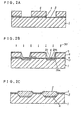
- FIG.1A a silicon dioxide layer 3 is formed over a substrate 1. Then, ion implanted regions 4 are formed by implanting impurities by using silicon nitride layers 2 as a mask. Then, selective local oxidation is carried out to form the field insulating regions 5 with their underlying channel stop regions 4 (see FIG.1B). The F + channel stop regions 4 are provided for obtaining high gate threshold voltage
- the formed cnannel stop regions 4 are extended to n + source and n a drain regions 15. F + -n + junctions are therefore formed therebetween and therefore Junction capacitance there increases. Such higher capacitance reduces the operation speed of MOS circuits constituted thereof.
- the channel stop regions 4 are also extended to underlying part of insulation layers 12 which are provided under the gate electrodes 13, and thus decrease gate width. Such narrowed gate width W 1 reduces current drive ability.
- method for making semiconductor device in accordance with the invention comprises the steps of:
- a semiconductor process described here is particularly suitable in ultra large scale integrated circuit.
- numerous specific details, such as specific layer thicknesses, etc., are set forth in order to provide a thorough understanding of the presently preferred process. However, it will be obvious to one skilled in the art that the invention may be practiced without these specific details.
- MOS metal-oxide-semiconductor
- the substrate 1 is a low conductivity substrate and is doped with a p-type dopant.
- a silicon dioxide layer 3 is formed by thermally oxidizing a surface of the substrate 1.
- a silicon nitride layer 2 as antioxidization layer is formed on the silicon dioxide layer 3 by C.V.D. (chemical vapor deposition) method.
- the silicon dioxide layer 3 is approximately 50 nm thick, and the silicon nitride layer 2 is approximately 120 nm thick.
- the silicon nitride layer 2 is patterned by using a photo-resist layer 6 as a mask.
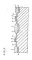
- a silanol film 7 which consists of silanol (H 3 SiOH) as principal ingredient is formed over the resist layer 6 and the substrate 1.
- the silanol film 7 can be formed by spine coating method in such a shape that thickness of the silanol film 7 in an edge 20a of an opening 20 is thicker than that in a center part 20b of the opening 20, when the silanol has viscosity of about 1 cp (centi poise).
- the silanol film 7 is heat-treated in about 300°C for 20 minutes to form a silicon dioxide layer 7.
- the formed silicon dioxide layer 7 has thicker part in the edge 20a of the opening 20 and thinner part in the center 20b of the opening 20.
- the thinner part 20b is about 100 nm thick.
- the substrate I is subject to impurity ion implantation as illustrated by lines 30, to form an ion implanting regions 4.
- Impurity ions are implanted into the substrate 1 through the center parts 20b of the openings 20, because in this part a thicknesses of the silicon dioxide layer 7 and the silicon dioxide layer 3 are thinner (about 150 nm) than the edge part 20a.
- the thicker part 20a of the silicon dioxide layer 7 prevents implantation the impurity ions into the substrate 1. Therefore, unnecessary spreading of the ion implanting regions 4 can be prevented.
- the resist layer 6 and the silicon dioxide layer 7 are removed by known process.
- LOCOS method are used to form the field insulating regions 5 with their underlying channel stop regions 4.
- MOS-LSI is produced.
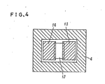
- the channel stop regions 4 are separated from the drain regions 14 and the source regions 15 and are not extended to the underlaying part of the insulation layers 12 provided under gate electrodes 13.
- the channel stop regions 4 are not formed over the edge of the field insulating regions 5 (see FIG.3). Therefore, undesirable junction capasitances between source and drain regions 14, 15 and the channel stop regions 4 are not increased. Such low chapasitances sives high speed to produced semiconductor.
- the gate width is not decreased since the ohannel stop region 4 are not extended to underlying part of insulation layers 12 (see FIG.4).
- the method for making semiconductor device in accordance with the present invention give high speed and high current drive ability to produced semiconductor device, as a result of introducing the forming step of the silanol film before the ion implanting step.
Landscapes
- Element Separation (AREA)
- Local Oxidation Of Silicon (AREA)
Applications Claiming Priority (2)
| Application Number | Priority Date | Filing Date | Title |
|---|---|---|---|
| JP68727/85 | 1985-04-01 | ||
| JP60068727A JPS61226942A (ja) | 1985-04-01 | 1985-04-01 | 半導体集積回路の素子間分離方法 |
Publications (3)
| Publication Number | Publication Date |
|---|---|
| EP0197454A2 true EP0197454A2 (de) | 1986-10-15 |
| EP0197454A3 EP0197454A3 (en) | 1990-11-07 |
| EP0197454B1 EP0197454B1 (de) | 1993-07-28 |
Family
ID=13382114
Family Applications (1)
| Application Number | Title | Priority Date | Filing Date |
|---|---|---|---|
| EP86104272A Expired - Lifetime EP0197454B1 (de) | 1985-04-01 | 1986-03-27 | Verfahren zur Herstellung von Halbleiteranordnungen mit Isolationszonen |
Country Status (4)
| Country | Link |
|---|---|
| US (1) | US4682408A (de) |
| EP (1) | EP0197454B1 (de) |
| JP (1) | JPS61226942A (de) |
| DE (1) | DE3688757T2 (de) |
Cited By (1)
| Publication number | Priority date | Publication date | Assignee | Title |
|---|---|---|---|---|
| EP0482829A1 (de) * | 1990-10-26 | 1992-04-29 | AT&T Corp. | Verfahren zur Herstellung eines compositen Oxyds auf einem hoch dotierten Bereich |
Families Citing this family (11)
| Publication number | Priority date | Publication date | Assignee | Title |
|---|---|---|---|---|
| US4968641A (en) * | 1989-06-22 | 1990-11-06 | Alexander Kalnitsky | Method for formation of an isolating oxide layer |
| US5378650A (en) * | 1990-10-12 | 1995-01-03 | Mitsubishi Denki Kabushiki Kaisha | Semiconductor device and a manufacturing method thereof |
| JP3134344B2 (ja) * | 1991-05-17 | 2001-02-13 | 日本電気株式会社 | 半導体装置 |
| JP3277533B2 (ja) * | 1992-01-08 | 2002-04-22 | ソニー株式会社 | 半導体装置の製造方法 |
| US5322804A (en) * | 1992-05-12 | 1994-06-21 | Harris Corporation | Integration of high voltage lateral MOS devices in low voltage CMOS architecture using CMOS-compatible process steps |
| US5675165A (en) * | 1994-08-02 | 1997-10-07 | Lien; Chuen-Der | Stable SRAM cell using low backgate biased threshold voltage select transistors |
| JP3335060B2 (ja) * | 1995-02-21 | 2002-10-15 | シャープ株式会社 | 半導体装置の製造方法 |
| FR2734403B1 (fr) * | 1995-05-19 | 1997-08-01 | Sgs Thomson Microelectronics | Isolement plan dans des circuits integres |
| DE19959346B4 (de) * | 1999-12-09 | 2004-08-26 | Micronas Gmbh | Verfahren zum Herstellen eines eine Mikrostruktur aufweisenden Festkörpers |
| DE50014168D1 (de) * | 2000-12-21 | 2007-04-26 | Micronas Gmbh | Verfahren zum herstellen eines eine mikrostruktur aufweisenden festkörpers |
| JP6027771B2 (ja) * | 2012-05-28 | 2016-11-16 | キヤノン株式会社 | 半導体装置、半導体装置の製造方法及び液体吐出装置 |
Family Cites Families (10)
| Publication number | Priority date | Publication date | Assignee | Title |
|---|---|---|---|---|
| JPS5228550B2 (de) * | 1972-10-04 | 1977-07-27 | ||
| JPS5253679A (en) * | 1975-10-29 | 1977-04-30 | Hitachi Ltd | Productin of semiconductor device |
| US4502208A (en) * | 1979-01-02 | 1985-03-05 | Texas Instruments Incorporated | Method of making high density VMOS electrically-programmable ROM |
| JPS5754343A (en) * | 1980-09-19 | 1982-03-31 | Matsushita Electric Ind Co Ltd | Formation of inversion preventing region |
| JPS58134443A (ja) * | 1982-02-04 | 1983-08-10 | Toshiba Corp | 半導体装置の製造方法 |
| GB2123605A (en) * | 1982-06-22 | 1984-02-01 | Standard Microsyst Smc | MOS integrated circuit structure and method for its fabrication |
| JPS5992547A (ja) * | 1982-11-19 | 1984-05-28 | Hitachi Ltd | アイソレ−シヨン方法 |
| JPS59136935A (ja) * | 1983-01-27 | 1984-08-06 | Nec Corp | 半導体装置の製造方法 |
| US4570325A (en) * | 1983-12-16 | 1986-02-18 | Kabushiki Kaisha Toshiba | Manufacturing a field oxide region for a semiconductor device |
| JPS60161671A (ja) * | 1984-02-01 | 1985-08-23 | Sanyo Electric Co Ltd | Mos半導体装置の製造方法 |
-
1985
- 1985-04-01 JP JP60068727A patent/JPS61226942A/ja active Pending
-
1986
- 1986-03-27 EP EP86104272A patent/EP0197454B1/de not_active Expired - Lifetime
- 1986-03-27 DE DE86104272T patent/DE3688757T2/de not_active Expired - Fee Related
- 1986-04-01 US US06/846,736 patent/US4682408A/en not_active Expired - Fee Related
Cited By (1)
| Publication number | Priority date | Publication date | Assignee | Title |
|---|---|---|---|---|
| EP0482829A1 (de) * | 1990-10-26 | 1992-04-29 | AT&T Corp. | Verfahren zur Herstellung eines compositen Oxyds auf einem hoch dotierten Bereich |
Also Published As
| Publication number | Publication date |
|---|---|
| DE3688757D1 (de) | 1993-09-02 |
| EP0197454A3 (en) | 1990-11-07 |
| JPS61226942A (ja) | 1986-10-08 |
| DE3688757T2 (de) | 1993-10-28 |
| US4682408A (en) | 1987-07-28 |
| EP0197454B1 (de) | 1993-07-28 |
Similar Documents
| Publication | Publication Date | Title |
|---|---|---|
| US4788160A (en) | Process for formation of shallow silicided junctions | |
| US6043157A (en) | Semiconductor device having dual gate electrode material and process of fabrication thereof | |
| US5918133A (en) | Semiconductor device having dual gate dielectric thickness along the channel and fabrication thereof | |
| EP0476380B1 (de) | Selbstjustierte Bipolartransistorstruktur und deren Herstellungsprozess | |
| US5013678A (en) | Method of making an integrated circuit comprising load resistors arranged on the field oxide zones which separate the active transistor zones | |
| US5397715A (en) | MOS transistor having increased gate-drain capacitance | |
| US5294822A (en) | Polycide local interconnect method and structure | |
| US4891326A (en) | Semiconductor device and a process for manufacturing the same | |
| US5047356A (en) | High speed silicon-on-insulator device and process of fabricating same | |
| US4682408A (en) | Method for making field oxide region with self-aligned channel stop implantation | |
| US5543338A (en) | Method for manufacturing a semiconductor device using a semiconductor-on-insulator substrate | |
| US4488348A (en) | Method for making a self-aligned vertically stacked gate MOS device | |
| JP2924763B2 (ja) | 半導体装置の製造方法 | |
| EP0459398B1 (de) | Herstellungsverfahren eines Kanals in MOS-Halbleiteranordnung | |
| US6303420B1 (en) | Integrated bipolar junction transistor for mixed signal circuits | |
| US5242849A (en) | Method for the fabrication of MOS devices | |
| US4426766A (en) | Method of fabricating high density high breakdown voltage CMOS devices | |
| US5970331A (en) | Method of making a plug transistor | |
| US5489545A (en) | Method of manufacturing an integrated circuit having a charge coupled device and a MOS transistor | |
| US6071781A (en) | Method of fabricating lateral MOS transistor | |
| US6087238A (en) | Semiconductor device having reduced-width polysilicon gate and non-oxidizing barrier layer and method of manufacture thereof | |
| US4445270A (en) | Low resistance contact for high density integrated circuit | |
| KR0166991B1 (ko) | 반도체 장치 | |
| US5923984A (en) | Method of making enhancement-mode and depletion-mode IGFETS with different gate materials | |
| US5597757A (en) | Method of manufacturing a semiconductor device including bipolar and MOS transistors |
Legal Events
| Date | Code | Title | Description |
|---|---|---|---|
| PUAI | Public reference made under article 153(3) epc to a published international application that has entered the european phase |
Free format text: ORIGINAL CODE: 0009012 |
|
| AK | Designated contracting states |
Kind code of ref document: A2 Designated state(s): DE FR GB |
|
| PUAL | Search report despatched |
Free format text: ORIGINAL CODE: 0009013 |
|
| AK | Designated contracting states |
Kind code of ref document: A3 Designated state(s): DE FR GB |
|
| RHK1 | Main classification (correction) |
Ipc: H01L 21/76 |
|
| 17P | Request for examination filed |
Effective date: 19901210 |
|
| 17Q | First examination report despatched |
Effective date: 19910405 |
|
| GRAA | (expected) grant |
Free format text: ORIGINAL CODE: 0009210 |
|
| AK | Designated contracting states |
Kind code of ref document: B1 Designated state(s): DE FR GB |
|
| REF | Corresponds to: |
Ref document number: 3688757 Country of ref document: DE Date of ref document: 19930902 |
|
| ET | Fr: translation filed | ||
| PGFP | Annual fee paid to national office [announced via postgrant information from national office to epo] |
Ref country code: GB Payment date: 19940325 Year of fee payment: 9 |
|
| PGFP | Annual fee paid to national office [announced via postgrant information from national office to epo] |
Ref country code: FR Payment date: 19940330 Year of fee payment: 9 |
|
| PGFP | Annual fee paid to national office [announced via postgrant information from national office to epo] |
Ref country code: DE Payment date: 19940530 Year of fee payment: 9 |
|
| PLBE | No opposition filed within time limit |
Free format text: ORIGINAL CODE: 0009261 |
|
| STAA | Information on the status of an ep patent application or granted ep patent |
Free format text: STATUS: NO OPPOSITION FILED WITHIN TIME LIMIT |
|
| 26N | No opposition filed | ||
| PG25 | Lapsed in a contracting state [announced via postgrant information from national office to epo] |
Ref country code: GB Effective date: 19950327 |
|
| GBPC | Gb: european patent ceased through non-payment of renewal fee |
Effective date: 19950327 |
|
| PG25 | Lapsed in a contracting state [announced via postgrant information from national office to epo] |
Ref country code: FR Free format text: LAPSE BECAUSE OF NON-PAYMENT OF DUE FEES Effective date: 19951130 |
|
| PG25 | Lapsed in a contracting state [announced via postgrant information from national office to epo] |
Ref country code: DE Effective date: 19951201 |
|
| REG | Reference to a national code |
Ref country code: FR Ref legal event code: ST |