EP0195594B1 - Elektronenröhre - Google Patents
Elektronenröhre Download PDFInfo
- Publication number
- EP0195594B1 EP0195594B1 EP86301793A EP86301793A EP0195594B1 EP 0195594 B1 EP0195594 B1 EP 0195594B1 EP 86301793 A EP86301793 A EP 86301793A EP 86301793 A EP86301793 A EP 86301793A EP 0195594 B1 EP0195594 B1 EP 0195594B1
- Authority
- EP
- European Patent Office
- Prior art keywords
- electron
- tube according
- electron tube
- silicon oxide
- envelope
- Prior art date
- Legal status (The legal status is an assumption and is not a legal conclusion. Google has not performed a legal analysis and makes no representation as to the accuracy of the status listed.)
- Expired - Lifetime
Links
- VYPSYNLAJGMNEJ-UHFFFAOYSA-N Silicium dioxide Chemical compound O=[Si]=O VYPSYNLAJGMNEJ-UHFFFAOYSA-N 0.000 claims description 36
- 239000007789 gas Substances 0.000 claims description 21
- OAICVXFJPJFONN-UHFFFAOYSA-N Phosphorus Chemical compound [P] OAICVXFJPJFONN-UHFFFAOYSA-N 0.000 claims description 16
- 239000011248 coating agent Substances 0.000 claims description 15
- 238000000576 coating method Methods 0.000 claims description 15
- OKTJSMMVPCPJKN-UHFFFAOYSA-N Carbon Chemical compound [C] OKTJSMMVPCPJKN-UHFFFAOYSA-N 0.000 claims description 14
- 229910002804 graphite Inorganic materials 0.000 claims description 14
- 239000010439 graphite Substances 0.000 claims description 14
- LIVNPJMFVYWSIS-UHFFFAOYSA-N silicon monoxide Chemical class [Si-]#[O+] LIVNPJMFVYWSIS-UHFFFAOYSA-N 0.000 claims description 13
- NTHWMYGWWRZVTN-UHFFFAOYSA-N sodium silicate Chemical compound [Na+].[Na+].[O-][Si]([O-])=O NTHWMYGWWRZVTN-UHFFFAOYSA-N 0.000 claims description 11
- 238000010894 electron beam technology Methods 0.000 claims description 9
- 229910052710 silicon Inorganic materials 0.000 claims description 8
- 239000010703 silicon Substances 0.000 claims description 8
- 229910052751 metal Inorganic materials 0.000 claims description 7
- 239000002184 metal Substances 0.000 claims description 7
- 239000011230 binding agent Substances 0.000 claims description 5
- XUIMIQQOPSSXEZ-UHFFFAOYSA-N Silicon Chemical compound [Si] XUIMIQQOPSSXEZ-UHFFFAOYSA-N 0.000 claims description 4
- 239000004115 Sodium Silicate Substances 0.000 claims description 4
- 238000000354 decomposition reaction Methods 0.000 claims description 4
- -1 silicon alkoxide Chemical class 0.000 claims description 4
- 229910052911 sodium silicate Inorganic materials 0.000 claims description 4
- 150000003839 salts Chemical class 0.000 claims description 3
- 229910052814 silicon oxide Inorganic materials 0.000 claims description 2
- 150000003863 ammonium salts Chemical class 0.000 claims 1
- 239000007864 aqueous solution Substances 0.000 description 27
- 229960001231 choline Drugs 0.000 description 25
- 239000010408 film Substances 0.000 description 22
- 239000000725 suspension Substances 0.000 description 15
- 239000007787 solid Substances 0.000 description 13
- 238000000034 method Methods 0.000 description 12
- 235000019353 potassium silicate Nutrition 0.000 description 7
- 239000000470 constituent Substances 0.000 description 5
- WGTYBPLFGIVFAS-UHFFFAOYSA-M tetramethylammonium hydroxide Chemical compound [OH-].C[N+](C)(C)C WGTYBPLFGIVFAS-UHFFFAOYSA-M 0.000 description 5
- 230000002411 adverse Effects 0.000 description 4
- 230000000694 effects Effects 0.000 description 4
- 239000000243 solution Substances 0.000 description 4
- 238000005507 spraying Methods 0.000 description 4
- BOTDANWDWHJENH-UHFFFAOYSA-N Tetraethyl orthosilicate Chemical compound CCO[Si](OCC)(OCC)OCC BOTDANWDWHJENH-UHFFFAOYSA-N 0.000 description 3
- DSAJWYNOEDNPEQ-UHFFFAOYSA-N barium atom Chemical compound [Ba] DSAJWYNOEDNPEQ-UHFFFAOYSA-N 0.000 description 3
- 230000015572 biosynthetic process Effects 0.000 description 3
- 239000000919 ceramic Substances 0.000 description 3
- OEYIOHPDSNJKLS-UHFFFAOYSA-N choline Chemical compound C[N+](C)(C)CCO OEYIOHPDSNJKLS-UHFFFAOYSA-N 0.000 description 3
- 230000006866 deterioration Effects 0.000 description 3
- 239000000843 powder Substances 0.000 description 3
- 238000001179 sorption measurement Methods 0.000 description 3
- QGZKDVFQNNGYKY-UHFFFAOYSA-O Ammonium Chemical compound [NH4+] QGZKDVFQNNGYKY-UHFFFAOYSA-O 0.000 description 2
- 238000004438 BET method Methods 0.000 description 2
- LFQSCWFLJHTTHZ-UHFFFAOYSA-N Ethanol Chemical compound CCO LFQSCWFLJHTTHZ-UHFFFAOYSA-N 0.000 description 2
- ZRALSGWEFCBTJO-UHFFFAOYSA-N Guanidine Chemical compound NC(N)=N ZRALSGWEFCBTJO-UHFFFAOYSA-N 0.000 description 2
- BPQQTUXANYXVAA-UHFFFAOYSA-N Orthosilicate Chemical compound [O-][Si]([O-])([O-])[O-] BPQQTUXANYXVAA-UHFFFAOYSA-N 0.000 description 2
- 229910052788 barium Inorganic materials 0.000 description 2
- 238000010276 construction Methods 0.000 description 2
- 238000001035 drying Methods 0.000 description 2
- 238000010438 heat treatment Methods 0.000 description 2
- 238000004519 manufacturing process Methods 0.000 description 2
- 150000003867 organic ammonium compounds Chemical class 0.000 description 2
- 239000000126 substance Substances 0.000 description 2
- 229910014472 Ca—O Inorganic materials 0.000 description 1
- CHJJGSNFBQVOTG-UHFFFAOYSA-N N-methyl-guanidine Natural products CNC(N)=N CHJJGSNFBQVOTG-UHFFFAOYSA-N 0.000 description 1
- 229910000831 Steel Inorganic materials 0.000 description 1
- 238000010521 absorption reaction Methods 0.000 description 1
- 230000001133 acceleration Effects 0.000 description 1
- QVGXLLKOCUKJST-UHFFFAOYSA-N atomic oxygen Chemical compound [O] QVGXLLKOCUKJST-UHFFFAOYSA-N 0.000 description 1
- 230000009286 beneficial effect Effects 0.000 description 1
- 239000004020 conductor Substances 0.000 description 1
- 238000007865 diluting Methods 0.000 description 1
- SWSQBOPZIKWTGO-UHFFFAOYSA-N dimethylaminoamidine Natural products CN(C)C(N)=N SWSQBOPZIKWTGO-UHFFFAOYSA-N 0.000 description 1
- 235000019441 ethanol Nutrition 0.000 description 1
- 238000002474 experimental method Methods 0.000 description 1
- 239000011521 glass Substances 0.000 description 1
- 239000004615 ingredient Substances 0.000 description 1
- 229910052743 krypton Inorganic materials 0.000 description 1
- DNNSSWSSYDEUBZ-UHFFFAOYSA-N krypton atom Chemical compound [Kr] DNNSSWSSYDEUBZ-UHFFFAOYSA-N 0.000 description 1
- 239000007788 liquid Substances 0.000 description 1
- 239000000463 material Substances 0.000 description 1
- 239000001301 oxygen Substances 0.000 description 1
- 229910052760 oxygen Inorganic materials 0.000 description 1
- 239000002574 poison Substances 0.000 description 1
- 231100000614 poison Toxicity 0.000 description 1
- 231100000572 poisoning Toxicity 0.000 description 1
- 230000000607 poisoning effect Effects 0.000 description 1
- 150000003856 quaternary ammonium compounds Chemical class 0.000 description 1
- 229920006395 saturated elastomer Polymers 0.000 description 1
- 238000007789 sealing Methods 0.000 description 1
- 239000000377 silicon dioxide Substances 0.000 description 1
- 239000007921 spray Substances 0.000 description 1
- 239000010959 steel Substances 0.000 description 1
- 150000003512 tertiary amines Chemical class 0.000 description 1
- LFQCEHFDDXELDD-UHFFFAOYSA-N tetramethyl orthosilicate Chemical compound CO[Si](OC)(OC)OC LFQCEHFDDXELDD-UHFFFAOYSA-N 0.000 description 1
- 239000010409 thin film Substances 0.000 description 1
Images
Classifications
-
- H—ELECTRICITY
- H01—ELECTRIC ELEMENTS
- H01J—ELECTRIC DISCHARGE TUBES OR DISCHARGE LAMPS
- H01J29/00—Details of cathode-ray tubes or of electron-beam tubes of the types covered by group H01J31/00
- H01J29/86—Vessels; Containers; Vacuum locks
- H01J29/88—Vessels; Containers; Vacuum locks provided with coatings on the walls thereof; Selection of materials for the coatings
-
- H—ELECTRICITY
- H01—ELECTRIC ELEMENTS
- H01J—ELECTRIC DISCHARGE TUBES OR DISCHARGE LAMPS
- H01J29/00—Details of cathode-ray tubes or of electron-beam tubes of the types covered by group H01J31/00
- H01J29/94—Selection of substances for gas fillings; Means for obtaining or maintaining the desired pressure within the tube, e.g. by gettering
-
- H—ELECTRICITY
- H01—ELECTRIC ELEMENTS
- H01J—ELECTRIC DISCHARGE TUBES OR DISCHARGE LAMPS
- H01J7/00—Details not provided for in the preceding groups and common to two or more basic types of discharge tubes or lamps
- H01J7/14—Means for obtaining or maintaining the desired pressure within the vessel
- H01J7/18—Means for absorbing or adsorbing gas, e.g. by gettering
Definitions
- This invention relates to an electron tube according to the first part of claim 1, more particularly to an electron tube containing within its envelope a substance which improves the emission life of the cathode.
- a typical electron tube such as a color cathode ray tube (color CRT) is usually provided with a front panel having a phosphor screen on its inner surface, a funnel united with the panel and having conductive film on its inner surface, a neck united with the funnel and housing an electron gun, a shadow mask disposed in close proximity to the phosphor screen, and a magnetic inner shield which is assembled so as to be continuous with the shadow mask and extends along the inside face of the funnel.
- the phosphor screen comprises a phosphor layer consisting of at least phosphor dots or phosphor stripes emitting red, green and blue light and a metal backing layer formed on this layer.
- a metal getter film is formed on the inner surface of the funnel or the inner surface of the neck.
- the getter film absorbs the gases generated during operation of a color CRT from the various members described above which together constitute the color cathode ray tube, and thereby maintains the degree of vacuum.
- these gases collide with the cathode surfaces of the abovementioned cathodes, and poison the electron emissive material of these cathode surfaces, thereby adversely affecting their emission characteristics. Further, when the temperature of the cathode surfaces etc. falls as the cathode ray tube is switched off, these gases which were produced during operation are not only adsorbed on the getter film but are also adsorbed on the cathode surfaces, thereby poisoning the latter, and adversely affecting their emission characteristics.
- the principal constituents of the gases referred to above are H 2 0, CH 4 or the like.
- Water glass or sodium silicate is usually mixed with the graphite suspension mentioned earlier in order to strengthen the adhesion of the inner conductive film, of which the graphite suspension is the principal constituent, and this water glass, because of its great hygroscopicity, is a major source of gas production, which, as aforesaid, causes deterioration of the emission characteristics.
- the needs of construction of the neck diameter which is entailed by enlargement of the deflection angle of a color cathode ray tube, and the reduction in baking temperature in the exhaust process in order to shorten process time, make the deterioration in emission characteristics caused by the discharge gases mentioned above, and hence the reduction in emission life, still more marked.
- the emission life is a problem not only in color cathode ray tubes, but also in other electron tubes with a cathode, such as monochrome cathode ray tubes, travelling-wave tubes, magnetrons, klystrons, transmitting tubes and the like.
- EP-A-0 118 961 discloses a forming method for applying a graphite conductive film on the inner surface of the vacuum envelope, using a very small amount of Si0 2 as a binder for the major conductive material which is graphite conductive film, instead of the normally used water glass; but the function of the Si0 2 here is that of a binder only, and it is not suggested that it improves emission.
- the Si0 2 works to adhere the conductive film firmly onto the surface of the envelope and to render that conductive film hard.
- This invention seeks to provide an electron tube of excellent emission life characteristics, in which the electron emissivity of the electron beam- generating cathode surfaces is not adversely affected by the release of the gases referred to above, and which therefore will maintain the desired tube life characteristics over a long period.
- the invention consists in an electron tube, containing at least an electron-emitting cathode and at least one member with a surface suitably a conductive surface and/or an insulating surface within an evacuated envelope, wherein a porous layer of activated silicon oxide for controlling residual gases in the envelope is formed on at least a part of that surface.
- a cathode ray tube comprises an envelope comprising a panel, a funnel sealingly united with the panel, and a neck extending on the side opposite to the funnel: a phosphor screen formed on the inside face of the panel; an inner conductive film attached to the inside wall of the funnel and an electron gun for generating an electron beam, mounted at the neck and containing a cathode; wherein a layer of activated silicon oxide is provided on at least part of the inside of the envelope.
- activated silicon oxide silicon oxide which will adsorb and control residual gases within the evacuated envelope, in particular those gases with a negative action on cathode emission. This can be produced from organic salts of silicon. It is believed that it adheres to the wall of the evacuated envelope and part of the surface of each of the electrodes, in the form of a porous layer with numerous minute holes to enlarge active surfaces.
- the amount of activated silicon oxide is, in practice, from 1 to 50 mg, per liter of volume of the envelope. If it is less than 1 mg, its contribution to prolonging the emission life of the cathodes will be minimal, while its effect is saturated if it exceeds 50 mg.
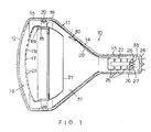
- Fig. 1 shows an embodiment of the invention.
- the evacuated envelope 11 of color cathode ray tube 10 consists of panel 12 of transparent glass curved into a substantially spherical surface, a funnel 14 of which one end face is sealingly attached to the skirt 13 of this panel 12, and a tubular neck 15 which is integrally attached to the tapered part of the other end of the funnel.
- a phosphor screen 16 is formed on the inner surface of panel 12.
- Screen 16 consists of a phosphor layer made up of successive stripes of phosphor which emit red, green, and blue light respectively, and a metal backing layer of A1 coated on to this layer.
- a shadow mask 17 consisting of a steel plate with numerous slit apertures 23 is disposed facing phosphor screen 16. Shadow mask 17 is supported at its periphery by a mask frame 18, and is demountably fixed by means of resilient supports 19 on support pin 20 anchored in skirt 13 of panel 12.
- a magnetic inner shield 21, extending on the electron gun side of the mask frame is fixed to mask frame 18.
- An electron gun 22 which generates electron beams is disposed inside neck 15. When the tube is operating, the electron beams pass through the apertures 23 in the shadow mask 17 and excite the phosphor layer of screen 16.
- electron gun 22 has three cathodes 25, 26 and 27 on the stem 24 side of neck 15. Electrons are emitted from the cathodes, forming three electron beams, which are accelerated and focussed by electrodes 28.
- the electron emissive surfaces of the cathodes constitute oxide cathodes of which the principal constituent is BaO.
- the internal wall of funnel 14 is covered with an inner conductive coating 31.
- This coating 31 is formed by coating the inner wall of funnel 14, by means of a spray or the like, with a liquid consisting of sodium silicate as a binding agent mixed with a graphite suspension, and then drying.
- a barium getter ring container 30, containing barium, is fixed by means of resilient metal element 29 to electron gun 22. This ring container 30 is positioned in the funnel when the electron gun 22 is fixed to the neck.
- the getter barium metal is evaporated inside the envelope onto the shadow mask, phosphor screen, etc., to increase the degree of vacuum of the envelope by absorbing residual gases.
- This activated Si0 2 can be formed by using a suspension in an aqueous solution of an organic ammonium silicate.
- An example of an aqueous solution of an organic ammonium silicate is an aqueous solution of Si0 2 - choline. This is formed by dissolving silica powder (Si0 2 ) in an aqueous solution of choline [HOCH 2 CH 2 N(CH 3 ) 3] OH-.
- the abovementioned aqueous solution of Si0 2 - choline can be applied to all the members with conductive surfaces or insulating surfaces inside the cathode ray tube that are principally irradiated by electron beams, namely the members forming the screen 16, shadow mask 17, inner shield 21, inner conductive coating 31, internal surface of the neck 15, electron gun 22 and getter support element 29.
- the aqueous solution of Si0 2 - choline may be used in place of some of the sodium silicate which is conventionally mixed as a binding agent with the graphite suspension in order to reinforce the adhesion of the inner conductive film 31 or the black heat-absorption layer (not shown in the drawing) formed on the metal backing constituting the phosphor screen 16. While the adhesion of the graphite suspension is maintained at the same level as in the conventional process, the activated Si0 2 formed by heat treatment enhances the emission life characteristics.
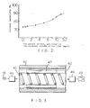
- Fig. 2 shows the residual emissivity after a 3000-hour forced emission life test and the solid Si0 2 content per liter of the internal volume.
- a solid Si0 2 content of at least 1 mg/I, and preferably at least 5 mg/I is required in order to secure better residual emissivity than the 70% obtained with conventional color cathode ray tubes.
- choline as the organic ammonium compound
- quaternary ammonium compounds such as tetramethylammonium hydroxide
- organic ammonium compounds such as tertiary amines, guanidine and the like
- silicon alkoxides such as tetramethylor- tho silicate, tetraethylortho silicate, Si(Opr n ) n and the like, can be used in this invention in the same way.
- a 10% Si0 2 -choline aqueous solution was prepared by dissolving 10% Si0 2 powder in a 10% aqueous solution of choline.
- the inner conductive coating 31 of funnel 14 was then coated with the 10% Si0 2 -choline aqueous solution by spraying.
- this aqueous solution decomposed, producing a thin, porous layer of activated silicon oxide.
- the amount of Si0 2 -choline aqueous solution used for the coating was, in terms of solid Si0 2 content, approximately 200 mg. In terms of the amount per liter of the internal volume of the 20 in.
- color cathode ray tube this is equivalent to approximately 10 mg/I.
- the residual emissivity of the Ba-Ca-O oxide cathode used in the electron gun proved to be 88%, a major improvement over the conventional 73%.
- the withstand voltage property (evaluated by the number of discharge sparks per minute when a forced acceleration voltage of 30 kV is applied) of these 20 in.
- a coating of a 10% Si0 2 -choline aqueous solution prepared as in Embodiment 1 was applied by spraying onto conductive surfaces of a shadow mask assembly 17, 18 which had been preheated to approx. 80 °C.
- the amount of the coating used to form activated Si0 2 layers 17a, 18a on the shadow mask assembly of a 20 in. color cathode ray tube, in terms of solid Si0 2 was approx. 100 mg, which is equivalent to 5 mg of solid Si0 2 per liter of internal volume of the 20 in. color cathode ray tube.
- the result of the same emission life test that was applied to Embodiment 1 was a figure for residual emissivity of 86%, an improvement similar to that of Embodiment 1.
- An adsorption area of at least twice the surface area of the underlying shadow mask can be obtained using the activated film obtained in the manner described above.
- a Kr (krypton) adsorption test performed using the BET method showed that the specific surface area of the film produced was 1.1 m 2 /g. This corresponds to a value of about 30 times the underlying area.
- a magnetic inner shield 21 was sprayed with 10% Si0 2 -choline aqueous solution by the same method as in Embodiment 2.
- the amount of the coating used on the magnetic inner shield of a 20 in. color cathode ray tube, in terms of solid Si0 2 was approx. 50 mg, which is equivalent to approx. 2.5 mg per liter of internal volume of the 20 in. color cathode ray tube.
- the result of the same emission life test that gas applied to Embodiment 2 was an improvement in residual emissivity to 82%.
- the amount of the coating used on the electron gun of a 20 in. color cathode ray tube, in terms of solid Si0 2 was approx. 50 mg, which is equivalent to approx. 2.5 mg per liter of internal volume of the 20 in. color cathode ray tube.
- the result of the same emission life test that was applied to Embodiment 1 was an improvement in residual emissivity to 82%.
- a suspension of which the principal constituent was graphite i.e. the graphite suspension used to form the inner conductive coating 31 of the tube, was prepared but with part of the water glass content of the suspension replaced by Si0 2 -choline aqueous solution.
- the weight ratio of solid Si0 2 to the total solid content of the suspension was set at 20%. Of this 20%, 4% derived from the Si0 2 - choline aqueous solution and 16% from the water glass.
- the internal surface of funnel 14 was coated with this graphite suspension by spraying. The thickness of the film was controlled so that the amount of graphite suspension used in a 20in.
- color cathode ray tube was such that the solid Si0 2 deriving from the Si0 2 -choline aqueous solution was approx. 100 mg for one cathode ray tube, equivalent to approx. 5 mg per liter of internal volume of the 20in. color cathode ray tube.
- 20 in. color cathode ray tubes were manufactured by the usual process, and subjected to the 3000- hour forced emission life test, residual emissivity improved to 89%.
- the specific surface area of the inner conductive film formed by the aforesaid graphite suspension according to this embodiment of the invention was calculated from the amount of N 2 adsorbed at low pressure (about 10- 5 Torr) by the BET method, it was found to be 30 m 2 /g.
- the specific surface area of an inner conductive film formed with a suspension using waterglass only was 6 m /g.
- the formation, according this embodiment of the invention, of activated Si0 2 resulted in the surface area being increased by a factor of 5 relative to the surface area obtained using waterglass only.
- the invention was applied to color cathode ray tubes.
- the invention can, however, also be applied to cathode ray tubes which do not use a shadow mask, such as monochrome cathode ray tubes, projection cathode ray tubes and the like.
- the application of the Si0 2 -choline aqueous solution need not be restricted to a single member.
- the effect of the invention can be obtained, provided the total amount of solid Si0 2 applied to the plurality of members of which the inside of a cathode ray tube consists is at least 1 mg per liter of the internal volume of the cathode ray tube.
- a silicon alkoxide solution in this embodiment an ethyl silicate solution, was prepared by diluting 10 parts of ethyl silicate, as main constituent, with 90 parts of ethyl alcohol. This silicon alkoxide solution was sprayed onto an inner conductive coating prepared as in Embodiment 6. After drying, the tube was subjected to the envelope sealing process and baking process at 430 ° C, This resulted in the formation of a film of activated porous Si0 2 . The amount of the Si0 2 was about 150 mg.
- the residual emission life of a tube manufactured in this way was 88% after a 3000 hour test.
- Fig. 3 depicts an embodiment in which the invention is applied to a traveling-wave tube.
- a helical delay line is fixed by means of three ceramic support rods 42 about the axis of a tubular evacuated envelope.
- Microwaves input from an input terminal 45 are amplified in a process in which electrons emitted from electron gun 43 are collected by collecter 44, and the amplified microwaves are output from an output terminal 46.
- the middle part of each of the ceramic support rods 42 is covered by an attenuator 47.
- Si0 2 -choline solution was mixed in with the attenuation layer when this layer was being applied, resulting in a layer 47 with an admixture of activated Si0 2 .
- the effect of the activated Si0 2 can be further enhanced by application of the coating to the inner wall of the envelope, the collector (anode) with a conductive surface, and those parts of the ceramic support rods with insulating surfaces not covered by the attenuators.
- the invention can also be applied to other electron tubes, such as a Klystron, magnetron, or transmitting tube, which use oxide or other cathodes.
- the adoption of the invention makes it possible, by the provision inside the envelope of an electron tube of activated Si0 2 , to obtain an electron tube, for example a color cathode ray tube, of outstanding emission life characteristics.
Landscapes
- Vessels, Lead-In Wires, Accessory Apparatuses For Cathode-Ray Tubes (AREA)
- Electrodes For Cathode-Ray Tubes (AREA)
- Cathode-Ray Tubes And Fluorescent Screens For Display (AREA)
- Formation Of Various Coating Films On Cathode Ray Tubes And Lamps (AREA)
Claims (12)
dadurch gekennzeichnet, daß eine poröse Schicht (17a) von aktiviertem Siliziumoxid zum Kontrollieren von Restgasen in dem Röhrenkolben auf mindestens einem Teil der Oberfläche gebildet ist.
Priority Applications (1)
| Application Number | Priority Date | Filing Date | Title |
|---|---|---|---|
| IN193/MAS/86A IN167144B (de) | 1986-03-12 | 1986-03-17 |
Applications Claiming Priority (2)
| Application Number | Priority Date | Filing Date | Title |
|---|---|---|---|
| JP60052183A JP2515278B2 (ja) | 1985-03-18 | 1985-03-18 | 電子管 |
| JP52183/85 | 1985-03-18 |
Publications (3)
| Publication Number | Publication Date |
|---|---|
| EP0195594A2 EP0195594A2 (de) | 1986-09-24 |
| EP0195594A3 EP0195594A3 (en) | 1989-03-08 |
| EP0195594B1 true EP0195594B1 (de) | 1992-07-29 |
Family
ID=12907688
Family Applications (1)
| Application Number | Title | Priority Date | Filing Date |
|---|---|---|---|
| EP86301793A Expired - Lifetime EP0195594B1 (de) | 1985-03-18 | 1986-03-12 | Elektronenröhre |
Country Status (6)
| Country | Link |
|---|---|
| US (1) | US4771214A (de) |
| EP (1) | EP0195594B1 (de) |
| JP (1) | JP2515278B2 (de) |
| KR (1) | KR900002907B1 (de) |
| CN (1) | CN1007191B (de) |
| DE (1) | DE3686186T2 (de) |
Families Citing this family (15)
| Publication number | Priority date | Publication date | Assignee | Title |
|---|---|---|---|---|
| KR940004076Y1 (ko) * | 1991-07-02 | 1994-06-17 | 삼성전관 주식회사 | 칼라브라운관의 인너실드 구조 |
| US5519283A (en) * | 1994-11-16 | 1996-05-21 | Thomson Consumer Electronics, Inc. | Internal magnetic shield for a color cathode-ray tube |
| IL116092A (en) * | 1994-11-30 | 2000-06-29 | Honeywell Inc | Ultraviolet transparent binder for phosphor fluorescent light box |
| US5838118A (en) * | 1996-03-28 | 1998-11-17 | Lucent Technologies Inc. | Display apparatus with coated phosphor, and method of making same |
| KR19990072194A (ko) * | 1996-10-11 | 1999-09-27 | 요트.게.아. 롤페즈 | 컬러음극선관및컬러선택전극제조방법 |
| US6069441A (en) * | 1996-10-31 | 2000-05-30 | Honeywell Inc. | Method for producing phospher binding materials |
| KR20000069190A (ko) * | 1997-09-29 | 2000-11-25 | 요트.게.아. 롤페즈 | 반도체 캐소드를 구비한 음극선관 |
| US6369499B1 (en) * | 1999-11-03 | 2002-04-09 | Intel Corporation | Electron gun with improved cathode venting |
| JP3509778B2 (ja) * | 2001-06-01 | 2004-03-22 | ソニー株式会社 | 陰極線管及び陰極線管の製造方法 |
| US6806557B2 (en) | 2002-09-30 | 2004-10-19 | Motorola, Inc. | Hermetically sealed microdevices having a single crystalline silicon getter for maintaining vacuum |
| US6929974B2 (en) * | 2002-10-18 | 2005-08-16 | Motorola, Inc. | Feedthrough design and method for a hermetically sealed microdevice |
| US6867543B2 (en) * | 2003-03-31 | 2005-03-15 | Motorola, Inc. | Microdevice assembly having a fine grain getter layer for maintaining vacuum |
| US7446601B2 (en) * | 2003-06-23 | 2008-11-04 | Astronix Research, Llc | Electron beam RF amplifier and emitter |
| US7045868B2 (en) * | 2003-07-31 | 2006-05-16 | Motorola, Inc. | Wafer-level sealed microdevice having trench isolation and methods for making the same |
| CN107120435B (zh) * | 2017-03-28 | 2018-09-21 | 嘉兴日雅光电有限公司 | 一种电子枪维护用真空密封装置 |
Family Cites Families (7)
| Publication number | Priority date | Publication date | Assignee | Title |
|---|---|---|---|---|
| US3792300A (en) * | 1972-07-15 | 1974-02-12 | Gte Sylvania Inc | Cathode ray tube having a conductive metallic coating therein |
| NL7605149A (nl) * | 1976-05-14 | 1977-11-16 | Philips Nv | Gasbindinrichting; werkwijze voor het vervaardi- gen van een kleurentelevisiebeeldbuis onder toe- passing van deze gasbindinrichting en alsdus ver- vaardigde kleurentelevisiebeeldbuis. |
| JPS5937037B2 (ja) * | 1978-11-09 | 1984-09-07 | 株式会社東芝 | 螢光体の製造方法 |
| DE3070123D1 (en) * | 1979-10-25 | 1985-03-21 | Toshiba Kk | Getter device |
| JPS5750753A (en) * | 1980-09-12 | 1982-03-25 | Hitachi Ltd | Color picture tube |
| NL8201750A (nl) * | 1982-04-28 | 1983-11-16 | Philips Nv | Inrichting voorzien van een geevacueerd vat met een getter en een getterhulpmiddel. |
| NL8300914A (nl) * | 1983-03-14 | 1984-10-01 | Philips Nv | Elektrische ontladingsbuis en werkwijze voor het vervaardigen van een elektrisch geleidende laag op een wandgedeelte van de omhulling van een dergelijke buis. |
-
1985
- 1985-03-18 JP JP60052183A patent/JP2515278B2/ja not_active Expired - Lifetime
-
1986
- 1986-03-05 CN CN86101366A patent/CN1007191B/zh not_active Expired
- 1986-03-10 US US06/837,831 patent/US4771214A/en not_active Expired - Lifetime
- 1986-03-12 EP EP86301793A patent/EP0195594B1/de not_active Expired - Lifetime
- 1986-03-12 DE DE8686301793T patent/DE3686186T2/de not_active Expired - Lifetime
- 1986-03-17 KR KR1019860002005A patent/KR900002907B1/ko not_active Expired
Also Published As
| Publication number | Publication date |
|---|---|
| EP0195594A3 (en) | 1989-03-08 |
| DE3686186T2 (de) | 1993-01-07 |
| CN86101366A (zh) | 1987-03-04 |
| DE3686186D1 (de) | 1992-09-03 |
| JPS61211944A (ja) | 1986-09-20 |
| EP0195594A2 (de) | 1986-09-24 |
| KR860007712A (ko) | 1986-10-15 |
| US4771214A (en) | 1988-09-13 |
| CN1007191B (zh) | 1990-03-14 |
| KR900002907B1 (ko) | 1990-05-03 |
| JP2515278B2 (ja) | 1996-07-10 |
Similar Documents
| Publication | Publication Date | Title |
|---|---|---|
| EP0195594B1 (de) | Elektronenröhre | |
| US4734615A (en) | Color cathode ray tube | |
| US4551652A (en) | Display screen having aluminum phosphate barrier layer and method of manufacture | |
| US4884004A (en) | Color cathode-ray tube having a heat dissipative, electron reflective coating on a color selection electrode | |
| EP0144022A1 (de) | Farbbildröhre | |
| US2843777A (en) | Cathode-ray tubes | |
| US4457731A (en) | Cathode ray tube processing | |
| US3979632A (en) | Cathode ray tube having surface charge inhibiting means therein | |
| KR920005980B1 (ko) | 다공질층으로 덮힌 새도우 마스크를 가진 칼라수상관 | |
| JPH0317930A (ja) | カラーブラウン管の製造方法 | |
| US3589791A (en) | Processing of cathode-ray tubes | |
| US5519283A (en) | Internal magnetic shield for a color cathode-ray tube | |
| JPH023262B2 (de) | ||
| US4940440A (en) | Weak beam scanning of cathode ray tubes | |
| US3814966A (en) | Post-deflection acceleration type color cathode-ray tube | |
| US6121724A (en) | Color cathode ray tube with high resistance film in the electron gun | |
| JPS62272430A (ja) | カラ−ブラウン管 | |
| JP3130530B2 (ja) | 陰極線管の製造方法 | |
| JPS6313298B2 (de) | ||
| KR100244219B1 (ko) | 함침형 음극의 활성화 처리 방법 | |
| JP3184416B2 (ja) | 陰極線管の製造方法 | |
| JP2000306511A (ja) | 陰極線管の製造方法 | |
| KR100209612B1 (ko) | 음극선관용 게터 커버 | |
| JPS5851443A (ja) | 陰極線管の排気方法 | |
| JPH07211247A (ja) | 受像管 |
Legal Events
| Date | Code | Title | Description |
|---|---|---|---|
| PUAI | Public reference made under article 153(3) epc to a published international application that has entered the european phase |
Free format text: ORIGINAL CODE: 0009012 |
|
| 17P | Request for examination filed |
Effective date: 19860321 |
|
| AK | Designated contracting states |
Kind code of ref document: A2 Designated state(s): DE FR GB NL |
|
| PUAL | Search report despatched |
Free format text: ORIGINAL CODE: 0009013 |
|
| AK | Designated contracting states |
Kind code of ref document: A3 Designated state(s): DE FR GB NL |
|
| 17Q | First examination report despatched |
Effective date: 19901219 |
|
| GRAA | (expected) grant |
Free format text: ORIGINAL CODE: 0009210 |
|
| AK | Designated contracting states |
Kind code of ref document: B1 Designated state(s): DE FR GB NL |
|
| ET | Fr: translation filed | ||
| REF | Corresponds to: |
Ref document number: 3686186 Country of ref document: DE Date of ref document: 19920903 |
|
| PLBE | No opposition filed within time limit |
Free format text: ORIGINAL CODE: 0009261 |
|
| STAA | Information on the status of an ep patent application or granted ep patent |
Free format text: STATUS: NO OPPOSITION FILED WITHIN TIME LIMIT |
|
| 26N | No opposition filed | ||
| REG | Reference to a national code |
Ref country code: GB Ref legal event code: 746 Effective date: 19981008 |
|
| REG | Reference to a national code |
Ref country code: FR Ref legal event code: D6 |
|
| REG | Reference to a national code |
Ref country code: GB Ref legal event code: IF02 |
|
| PGFP | Annual fee paid to national office [announced via postgrant information from national office to epo] |
Ref country code: NL Payment date: 20050303 Year of fee payment: 20 |
|
| PGFP | Annual fee paid to national office [announced via postgrant information from national office to epo] |
Ref country code: FR Payment date: 20050308 Year of fee payment: 20 |
|
| PGFP | Annual fee paid to national office [announced via postgrant information from national office to epo] |
Ref country code: GB Payment date: 20050309 Year of fee payment: 20 |
|
| PGFP | Annual fee paid to national office [announced via postgrant information from national office to epo] |
Ref country code: DE Payment date: 20050310 Year of fee payment: 20 |
|
| PG25 | Lapsed in a contracting state [announced via postgrant information from national office to epo] |
Ref country code: GB Free format text: LAPSE BECAUSE OF EXPIRATION OF PROTECTION Effective date: 20060311 |
|
| PG25 | Lapsed in a contracting state [announced via postgrant information from national office to epo] |
Ref country code: NL Free format text: LAPSE BECAUSE OF EXPIRATION OF PROTECTION Effective date: 20060312 |
|
| REG | Reference to a national code |
Ref country code: GB Ref legal event code: PE20 |
|
| NLV7 | Nl: ceased due to reaching the maximum lifetime of a patent |
Effective date: 20060312 |