EP0195217B1 - Magnetic reluctance sensing apparatus and method - Google Patents
Magnetic reluctance sensing apparatus and method Download PDFInfo
- Publication number
- EP0195217B1 EP0195217B1 EP86101473A EP86101473A EP0195217B1 EP 0195217 B1 EP0195217 B1 EP 0195217B1 EP 86101473 A EP86101473 A EP 86101473A EP 86101473 A EP86101473 A EP 86101473A EP 0195217 B1 EP0195217 B1 EP 0195217B1
- Authority
- EP
- European Patent Office
- Prior art keywords
- reluctance
- flux
- sensor
- magnetic
- magnetic flux
- Prior art date
- Legal status (The legal status is an assumption and is not a legal conclusion. Google has not performed a legal analysis and makes no representation as to the accuracy of the status listed.)
- Expired
Links
- 238000000034 method Methods 0.000 title description 8
- 230000004907 flux Effects 0.000 claims description 52
- 230000008878 coupling Effects 0.000 claims description 26
- 238000010168 coupling process Methods 0.000 claims description 26
- 238000005859 coupling reaction Methods 0.000 claims description 26
- 239000000463 material Substances 0.000 claims description 12
- 230000035699 permeability Effects 0.000 claims description 5
- 239000011162 core material Substances 0.000 description 13
- 230000005415 magnetization Effects 0.000 description 12
- 230000008859 change Effects 0.000 description 6
- 239000004020 conductor Substances 0.000 description 5
- 238000009413 insulation Methods 0.000 description 5
- 230000035945 sensitivity Effects 0.000 description 5
- 239000000758 substrate Substances 0.000 description 5
- VYPSYNLAJGMNEJ-UHFFFAOYSA-N Silicium dioxide Chemical compound O=[Si]=O VYPSYNLAJGMNEJ-UHFFFAOYSA-N 0.000 description 4
- RTAQQCXQSZGOHL-UHFFFAOYSA-N Titanium Chemical compound [Ti] RTAQQCXQSZGOHL-UHFFFAOYSA-N 0.000 description 4
- 238000001514 detection method Methods 0.000 description 4
- 230000000694 effects Effects 0.000 description 4
- 230000001939 inductive effect Effects 0.000 description 4
- UGKDIUIOSMUOAW-UHFFFAOYSA-N iron nickel Chemical compound [Fe].[Ni] UGKDIUIOSMUOAW-UHFFFAOYSA-N 0.000 description 4
- 239000010936 titanium Substances 0.000 description 4
- 229910052719 titanium Inorganic materials 0.000 description 4
- 238000005516 engineering process Methods 0.000 description 3
- 238000005259 measurement Methods 0.000 description 3
- 230000007246 mechanism Effects 0.000 description 3
- 230000004044 response Effects 0.000 description 3
- 239000000126 substance Substances 0.000 description 3
- XEEYBQQBJWHFJM-UHFFFAOYSA-N Iron Chemical compound [Fe] XEEYBQQBJWHFJM-UHFFFAOYSA-N 0.000 description 2
- 229910001030 Iron–nickel alloy Inorganic materials 0.000 description 2
- 230000008021 deposition Effects 0.000 description 2
- 238000013461 design Methods 0.000 description 2
- 238000005530 etching Methods 0.000 description 2
- 230000001965 increasing effect Effects 0.000 description 2
- 238000002955 isolation Methods 0.000 description 2
- 229910052751 metal Inorganic materials 0.000 description 2
- 239000002184 metal Substances 0.000 description 2
- 235000012239 silicon dioxide Nutrition 0.000 description 2
- 239000000377 silicon dioxide Substances 0.000 description 2
- 229910052770 Uranium Inorganic materials 0.000 description 1
- 229910052782 aluminium Inorganic materials 0.000 description 1
- XAGFODPZIPBFFR-UHFFFAOYSA-N aluminium Chemical compound [Al] XAGFODPZIPBFFR-UHFFFAOYSA-N 0.000 description 1
- 238000013459 approach Methods 0.000 description 1
- 230000008901 benefit Effects 0.000 description 1
- 238000010276 construction Methods 0.000 description 1
- 230000003247 decreasing effect Effects 0.000 description 1
- 238000001914 filtration Methods 0.000 description 1
- 239000012212 insulator Substances 0.000 description 1
- 238000004519 manufacturing process Methods 0.000 description 1
- 230000000873 masking effect Effects 0.000 description 1
- 238000012986 modification Methods 0.000 description 1
- 230000004048 modification Effects 0.000 description 1
- 229920006395 saturated elastomer Polymers 0.000 description 1
- 230000032258 transport Effects 0.000 description 1
- 238000004804 winding Methods 0.000 description 1
Images

Classifications
-
- G—PHYSICS
- G01—MEASURING; TESTING
- G01R—MEASURING ELECTRIC VARIABLES; MEASURING MAGNETIC VARIABLES
- G01R33/00—Arrangements or instruments for measuring magnetic variables
- G01R33/12—Measuring magnetic properties of articles or specimens of solids or fluids
- G01R33/1223—Measuring permeability, i.e. permeameters
Definitions
- This invention relates to magnetic reluctance sensing devices in general and to magnetic sensors employed in reluctance sensing arrangements in particular.
- Inductive sensors exist in the known art and are applied to the task of sensing magnetic ink characters on bank checks, to pulse generation or timing applications. Such applications as ignition rotor position inductive sensing in automotive ignition systems and gear tooth counting in machine control applications, are also common, to name but a few. Inductive sensors rely on the time rate of change of flux brought about by increasing or decreasing the number of lines of flux intersecting an electrically conductive coil. These sensors require magnetized media or machine elements to be effective.
- reluctance sensors are capable of producing an output in the steady state, i.e., no relative motion between the sensor and the medium to be sensed, but rely upon precision measurements of variations in the drive coil current and/or voltage produced by changes in the magnetic reluctance path of a flux circuit.
- Yet another object of the invention is to provide an improved constant flux magneto resistive magnetic reluctance sensing apparatus in which an essentially constant magnetic flux is shared between the magnetic sensor and the object whose reluctance is to be sensed.
- Yet another object of the invention is to provide an improved magnetic reluctance sense head structure in which an essentially constant magnetic flux is passed through magnetic sensors in series or in parallel and variations are measured in the flux conducted through them produced by the presence or absence of the medium whose reluctance is to be sensed when it is inserted in a flux path.
- an essentially constant magnetic flux source applying a constant level of magnetic flux to a pair of sensing legs made of magnetically permeable material.
- the magnetically permeable legs may include magneto resistive magnetic sensing elements in series with them or may be bridged in parallel by a magneto resistive sensing element.
- the sensing element is either in a magnetic series or magnetically parallel circuit arrangement with the substance whose magnetic reluctance is to be sensed is placed in proximity to the tips or ends of the magnetically permeable conductive legs.
- a constant magnetic flux source is provided by a constant number of electrically conductive turns provided with a constant current in a coil surrounding a leg portion of the magnetically permeable structure.
- magnetic reluctance sensing is by no means limited to the application of sensing magnetic ink characters but may be extended to general magnetic sensing for pulse counting, timing and proximity measurements to name but a few.
- magnetic ink characters applied to bank checks for automatic reading exhibit a very poor magnetic remanence, in particular, when such characters are magnetized, the vertical field component available for sensing from the typical carbonyl iron ink material is very low.
- the normal detection mechanism for such magnetic ink characters utilizes magnetic inductive sensors.
- sensors due to the flux derivative sensing technique employed, high velocity transports and elaborate frequency filtering mechanisms are required to obtain even a minimum signal to noise ratio.
- the magnetic ink character materials do exhibit a relatively low magnetic reluctance path as opposed to air when subjected to a magnetic field.
- the average permeability (relative to plain air) for carbonyl iron is stated in the literature to be approximately 55 in the presence of a field of 210-3Wb/m2. Reluctance sensing is by far the preferred approach for detecting the presence of magnetic ink characters in view of this fact.
- the preferred embodiments of the invention disclosed herein utilize a reluctance sensing scheme employing a new coupled film magneto resistive sensor element in configuration with other elements in the preferred embodiment for measuring the effects of a differential reluctance created by the presence or absence of magnetic ink characters.
- the sensor itself will be described only briefly since other forms of magnetically sensitive elements might be used; namely, magnetically sensitive transistors, diodes, Hall cells, and the like, to name but a few.
- My commonly assigned co-pending application EP-A-0154005 describes the structural details of a suitable magneto resistive sensor as will be described briefly herein.
- the sensing technique employed in the present invention does not resort to the use of alternating magnetic fields for detecting the presence of magnetic ink characters, nor has it been found necessary to precondition the ink characters before attempting to sense their presence.
- Machine or hand scanning of bank checks utilizing this new technology produces the same results because the detection system is velocity insensitive. Even DC or steady state reluctance measurements are usually achieved.
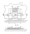
- FIG. 1A an overall pictorial schematic of a preferred embodiment of the present magnetic reluctance sensing head is shown in proximity to a cross section of an exemplary piece of paper having deposited on its surface a thickness of magnetically permeable ink.
- FIG. 1A The embodiment depicted in Figure 1A is constructed using photo lithographic deposition and etching techniques familiar to those of skill in the large scale integrated circuit arts. This technique is used to facilitate making the magnetic reluctance sensors of small size so that numerous sensors may be ganged together in parallel for sensing a whole array of characters. Consequently, the sensor is depicted as being deposited on the top surface of a semiconductive substrate 1.
- Two ended vertical coupling legs of the U or C-shaped member are shown as legs 2. These could be formed of nickel iron alloy typically of 1 11m thick or less and approximately 0,1 mm wide as shown by the dimension W L in Figure 1A.
- a magneto resistive sensor consisting of a pair of approximately 30 nm thick nickel iron films with an intermediate 25 nm thick titanium isolation layer 5 is shown as sensor 3.
- Sensor 3 is magnetically linked to the proximate ends of magnetically permeable legs 2 but is electrically isolated therefrom by a 500 nm thick silicon dioxide layer for example. This is shown as an underlying oxide layer 4 which is not apparent in Figure 1A but which separates the magnetically permeable legs 2 from actual electrical and physical contact with the coupled film magnetic sensor 3, as shown in Figure 1B.
- a gap 9 separates the magnetic flux core member 6 from the magnetically permeable legs 2.
- the purpose of the gap 9 is to make the reluctance path from the medium 13 at the distal ends of the permeable legs 2 through the core 6 of much higher reluctance than the path from the distal ends of the legs 2 through the sensor 3.
- the gap 9 also provides a means of delivering an essentially constant magnetic flux to be shared by the MR sensor 3 and material 13 whose reluctance is to be sensed when it is positioned adjacent the tips of the distal ends of legs 2 where material 13 acts essentially as a keeper path.
- magnetic ink 13 is deposited on a substrate of paper 12 which could be separated from the tips of legs 2 by a distance 10 on the order of a fraction to one or two microns.
- the magnetic ink layer 13 acts essentially as a magnetic keeper for the magnetic flux emanating from the distal ends of the permeable legs 2.
- the core member 6 is made of nickel iron alloy as are the permeable legs 2, and has deposited around it a conductive coil 7 consisting of N turns of conductive lines such as aluminum.
- a conductive coil 7 consisting of N turns of conductive lines such as aluminum.
- Appropriate oxide insulation would be formed over the top surface and bottom surface of the magnetically permeable core 6 in a manner well known in the art. Briefly, an oxide layer would be deposited on the substrate 1 and the first half of the conductors 7 as shown in dotted lines in Figure 1A would be laid down. These will be overlain with another insulation layer on which would be deposited the core material for core 6. Another layer of insulation would follow with etching through at the points where the conductors are to be joined.
- Typical dimensions for the sensor 3 would be 5 11m width and 12 to 15 11m length as shown in Figure 1A.
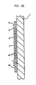
- Figure 1 B illustrates a cross sectional elevational view looking from the tips or distal ends of the legs 2 as shown in Figure 1A. It may be observed that electrical contacts A and B are made to the MR sensor 3 which consists of two layers of nickel iron film separated by an intermediate separator 5 in the zone where magnetic sensitivity is desired. As shown in Figure 1B, the zone of sensitivity of the MR sensor 3 is in the gap region between the two legs 2. The MR films 3 are joined electrically and mechanically in the region where they underlie the proximate ends of magnetically permeable legs 2. The contacts A and B are utilized to supply a sensing current Is on the order or 3 mA in the preferred embodiment.
- the reluctance path through the substance 13 will be greater or more than that through the MR sensor 3. Accordingly, sensor 3 will conduct more or less, respectively, of the flux coming from core 6.
- the resultant variation in conductivity of the MR sensor 3 can be observed through the contacts A and B to provide a direct indication of magnetic reluctance observed at the conductive leg 2 to medium 13 interface.
- a wide variety of other sensor technologies might be employed including magnetic transistors, Hall cells and the like.
- the magneto resistive sensor technology as depicted herein is superior in that it is most easily compatible with the construction techniques employed for creating the rest of the magnetic structure.
- the basic design of the reluctance measuring head is simple and it consists almost entirely of deposited magnetic film and insulation layers of a simple outline that may be easily masked and laid down. Typical dimensions for the structural components have been described above.
- the sensor is located at a relatively remote position from its interface with the paper bearing a magnetic ink character so that wear and fabrication and thermal effect problems are minimized.
- the MR sensor 3 consists of two parallel nickel iron film layers each having an easy axis of magnetization arranged perpendicular to the length L s of the overall sensor 3 bridging the proximate ends of vertical coupling legs 2.
- the two layers of the MR sensor 3 are magneto statically coupled along the direction of easy axis as shown in Figures 1A and 2.
- a low conductivity metal film isolation layer on the order of 20 to 35 nm thick, is chosen to be titanium in Figures 1A and 1 B. This is shown as the layer 5.
- the low conductivity metal does not seriously detract from the sensor current Is and prevents magnetic exchange coupling mechanisms from occurring between the two films that form the sensor 3.
- the current Is produces a voltage deep across the magneto resistive element 3 which is modified by changes in resistance influenced by the change in the proportion of flux conducted by the sensor which are brought about by changes in reluctance via coupling to the medium 13 occurring at the distal ends of the vertical coupling legs 2.
- the variation in circuit reluctance at the distal ends of the coupling legs 2 results in a proportional change in the magnetic flux passing through sensor3 and in the overall magnetization vector at rest in the MR films 3 which modifies the overall electrical resistivity of each MR film layer in a manner well known in the art.
- the sensitive portion of sensor 3 lies between the vertical legs 2.
- the coupled film sensor 3 is insulated from the legs 2 by the silicon dioxide insulation layer 4.
- the thickness of each of the magneto resistive layers 3 is required to be identical and is typically 30 nm.
- the height and width of each film layer should also be equal since these dimensions also control the overall reluctance of the sensor itself.
- MR sensors of the type described are deposited in the presence of an intense magnetic field oriented to produce an easy magnetic axis in the chosen direction. In the case at hand, the easy magnetic axis is chosen to be perpendicular to the length L s of the overall sensor 3.
- the current I supplied to the magnetizing coil 7 creates a magnetic flux that couples through the air gap 9 to the proximate ends of the vertical coupling legs 2 and through the MR sensor leg 3 where it torques the magnetization within the MR films toward the hard axis (horizontal in Figure 1A and 2).
- the MR sensor 3 becomes saturated when magnetization within the films is forced to lie parallel with the hard magnetic axis.
- the electrical current passing down the MR sensor films shown as Is tends to torque the magnetization within the sensor films back toward the easy axis. In operation then, current is passed through the magnetizing coil 7 such that magnetization within both film layers 3 is caused to uniformly rotate toward the hard magnetic axis.
- the electrical current Is conducted by each layer of the sensor 3 prevents the magnetization vector from fully reaching the hard axis.
- the device will have greatest sensitivity when the magnetization vector is close to the hard axis and the least sensitivity when the magnetization vector is closer to the easy axis.
- Figure 2 illustrates a slightly modified version of the structure shown in Figure 1A.
- the modified structure minimizes the ambiguous state of magnetization within the MR leg 3 in the area located under the vertical leg members 2.
- Field coupling from the legs 2 to the MR sensor 3 is improved by flux concentration effects produced by necking down legs 2 where they cross over sensor 3 and the effective length of the MR sensor is increased leading to at least a 20% increase in signal amplitude because the reduced width of legs 2 leaves more active area for sensor 3 along length L s .
- the sensor head-to-check height is depicted as a dimension 10. With the head-to-check height varied from 0 to a 25 ⁇ m space, the signal response is calculated to be 600 uV when the legs 2 are in contact with magnetic ink layer 13, 370 ⁇ V when a 6 micron space for dimension 10 exists, and 240 uV when a 25 micron space is present.
- a current density J of 1 x 10 6 A/Cm 2 flowing through the sensor 3.
- a magnetizing coil current of approximately 40 mA and a 5 turn coil as depicted in the figures is assumed.
- the magnetic ink permeability is assumed to be 55 at 2 10 -3 Wb/m 2 and the MR sensor resistance is approximately 27 Ohms.
- a 3 mA sensor current is included.
- the power dissipated by the sensor is thus approximately 243 uw. Shot noise will be on the order of .26 pV with a 100,000 cycle bandwidth.
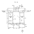
- FIG. 3A An improved form of the sensor is depicted in Figure 3A.
- the sensor 3 from Figure 1A is replaced by two sensors, 3A and 3B, in this Figure 3A.
- the sensors are now in series with the magnetically conductive legs 2A and 2B instead of shunting or bridging the legs 2 as shown in Figure 1A.
- the structure in Figures 3A and 3B illustrates an alternative embodiment that has a much higher sensitivity than the structure shown in Figures 1A and 1 B and 2.
- This head structure is capable of adequately sensing thin magnetic ink with a permeability as low as 4 instead of the assumed 55 and at an altitude of 50 11 m above the check surface instead of the normal altitude of 6 to 12 11 m assumed for the earlier embodiment.
- Figure 3A the basic design of this embodiment is similar to that in Figure 1 in that most of the elements are constructed utilizing film masking and deposition steps familiar to those of skill in the LSI and circuit arts. Similar elements are similarly numbered in Figures 1A, 1 B, 2 and 3A so that independent discussion of each of them such as the core 6 is unnecessary unless differences in structure or operation exist. The differences will be addressed herein.
- FIG. 3A The basic structure depicted in Figure 3A has an inverted U-shape. Coupled film magneto resistive elements 3A and 3B form part of each vertical coupling leg 2 in this structure. Magnetizing coil 7 similar to that in the other figures encircles the top cross member and energizes the MR sensors 3A and 3B and applies a flux to the gap at the ends of the coupling legs 2A and 2B. It is evident from Figure 3A that the width of the MR sensor legs 3A and 3B is less than the width of a 1 11 m thick nickel iron coupling legs 2A and 2B. It may be shown that the width of the MR sensors 3A and 3B dramatically influences the magnitude of the current required by the magnetizing coil 7 but has nothing whatever to do with the overall signal amplitude.
- the sensors 3A and 3B in each leg 2 of the structure consist of a pair of parallel uniaxial magnetic films of the same form, structure and overall dimension as those depicted and described with reference to Figure 1A and 1B.
- the two MR sensors 3A and 3B are connected in series with connector 11 and the current Is is passed between the contacts A and B as previously described.
- the voltage developed between terminals A and B due to the resistance changes is that required to maintain the constant current Is.
- the variation in voltage is a measure of the differential flux passing through the MR legs 3A and 3B and ultimately is a measure of the reluctance of the material that may be introduced in the sensor gap at the ends of the legs 2A and 2B.
- the operation of the reluctance sensing device depends upon the fundamental principle that the product of flux flowing around a closed loop and the reluctance R of the loop is proportional to the number of current turns encircling the loop.
- the closed loop reluctance drops compared to having air in the gap.
- the magnetic flux flowing in the closed loop must increase for a given current since the product of current times turns is constant.
- the sensor current Is is conducted by a nonmagnetic conductive leg 11 bridging the gap between the distal ends of legs 2A and 2B and electrically insulated from them by the oxide layer 4 seen to better advantage in the cross section in Figure 3B.
- the titanium layer 5 separates the two films of a sensor 3A as shown in this figure. At points C in each leg 2, however, the titanium layer is omitted and the MR films come in direct physical and electrical contact with one another.
- One of these joints C in one leg 2A is connected via the conductor 11 shown in Figure 3A to its counterpart in the sensor occupying the other leg 2B of the structure shown in Figure 3A. Because the electrically conductive member 11 is not magnetically conductive, it does not shunt any of the magnetic flux from core member 6 nor does it interact with the magnetic operation in any way.
- the preferred embodiments of magnetic reluctance sensing apparatus and the method of employing magnetic sensors either in shunt or in series with the material whose reluctance is to be sensed are generally applicable to a variety of reluctance sensing tasks.
- the nature of the task may dictate the form of the structure of the coupling members, the orientation of the sensor and the magnitudes of the various currents and voltages experienced, but will not alter the overall mode of operation and basic structure of the sensors and reluctance detecting elements. Therefore, numerous modifications in form and structure can easily be made to suit a given application without departing from the scope of the invention as defined in the appended claims.
Landscapes
- Physics & Mathematics (AREA)
- Condensed Matter Physics & Semiconductors (AREA)
- General Physics & Mathematics (AREA)
- Inspection Of Paper Currency And Valuable Securities (AREA)
- Measurement Of Length, Angles, Or The Like Using Electric Or Magnetic Means (AREA)
- Measuring Magnetic Variables (AREA)
- Magnetic Heads (AREA)
- Investigating Or Analyzing Materials By The Use Of Magnetic Means (AREA)
Applications Claiming Priority (2)
| Application Number | Priority Date | Filing Date | Title |
|---|---|---|---|
| US711864 | 1985-03-14 | ||
| US06/711,864 US4668913A (en) | 1985-03-14 | 1985-03-14 | Constant flux magneto resistive magnetic reluctance sensing apparatus |
Publications (2)
| Publication Number | Publication Date |
|---|---|
| EP0195217A1 EP0195217A1 (en) | 1986-09-24 |
| EP0195217B1 true EP0195217B1 (en) | 1990-12-27 |
Family
ID=24859853
Family Applications (1)
| Application Number | Title | Priority Date | Filing Date |
|---|---|---|---|
| EP86101473A Expired EP0195217B1 (en) | 1985-03-14 | 1986-02-05 | Magnetic reluctance sensing apparatus and method |
Country Status (5)
| Country | Link |
|---|---|
| US (1) | US4668913A (cg-RX-API-DMAC10.html) |
| EP (1) | EP0195217B1 (cg-RX-API-DMAC10.html) |
| JP (1) | JPS61213781A (cg-RX-API-DMAC10.html) |
| CA (1) | CA1241058A (cg-RX-API-DMAC10.html) |
| DE (1) | DE3676520D1 (cg-RX-API-DMAC10.html) |
Families Citing this family (32)
| Publication number | Priority date | Publication date | Assignee | Title |
|---|---|---|---|---|
| JPH07105006B2 (ja) * | 1985-11-05 | 1995-11-13 | ソニー株式会社 | 磁気抵抗効果型磁気ヘツド |
| US4771349A (en) * | 1986-10-31 | 1988-09-13 | International Business Machine Corporation | Magnetoresistive read transducer |
| US5159511A (en) * | 1987-04-01 | 1992-10-27 | Digital Equipment Corporation | Biasing conductor for MR head |
| US4885649A (en) * | 1987-04-01 | 1989-12-05 | Digital Equipment Corporation | Thin film head having a magneto-restrictive read element |
| US5089334A (en) * | 1988-08-03 | 1992-02-18 | Digital Equipment Corporation | Flux spreading thin film magnetic devices |
| US5085935A (en) * | 1988-08-03 | 1992-02-04 | Digital Equipment Corporation | Flux spreading thin film magnetic devices |
| CA1334447C (en) * | 1988-08-03 | 1995-02-14 | Digital Equipment Corporation | Perpendicular anisotropy in thin film devices |
| JP2728487B2 (ja) * | 1989-02-08 | 1998-03-18 | 株式会社日立製作所 | 録再分離複合型磁気ヘッド |
| US5195005A (en) * | 1989-06-02 | 1993-03-16 | Digital Equipment Corporation | Tranducer with improved inductive coupling |
| US5428893A (en) * | 1989-06-02 | 1995-07-04 | Quantum Corporation | Method of making a transducer with improved inductive coupling |
| US5311386A (en) * | 1989-06-02 | 1994-05-10 | Digital Equipment Corporation | Transducer with improved inductive coupling |
| US5184267A (en) * | 1989-06-02 | 1993-02-02 | Digital Equipment Corporation | Transducer with improved inductive coupling |
| US5084794A (en) * | 1990-03-29 | 1992-01-28 | Eastman Kodak Company | Shorted dual element magnetoresistive reproduce head exhibiting high density signal amplification |
| US5258884A (en) * | 1991-10-17 | 1993-11-02 | International Business Machines Corporation | Magnetoresistive read transducer containing a titanium and tungsten alloy spacer layer |
| US5293125A (en) * | 1992-01-17 | 1994-03-08 | Lake Shore Cryotronics, Inc. | Self-aligning tachometer with interchangeable elements for different resolution outputs |
| US5331496A (en) * | 1992-02-14 | 1994-07-19 | Digital Equipment Corporation | Thin-film magnetic transducer with a multitude of magnetic flux interactions |
| US5315246A (en) * | 1992-08-19 | 1994-05-24 | Eastman Kodak Company | Rotating source for generating a magnetic field for use with a currency detector |
| US5336994A (en) * | 1992-11-20 | 1994-08-09 | Lake Shore Cryotronics, Inc. | Magneto-resistive tachometer assembly with reversible cover and related method |
| US5495758A (en) * | 1993-06-17 | 1996-03-05 | Lake Shore Cryotronics, Inc. | Tachometer assembly with integral internal wrench |
| DE4326029C2 (de) * | 1993-08-03 | 1995-05-24 | Amphenol Tuchel Elect | Leser für Informationskarten |
| US5514955A (en) * | 1994-03-11 | 1996-05-07 | Lake Shore Cryotronics, Inc. | Slim profile digital tachometer including planar block and rotor having spokes and clamp |
| JPH07270507A (ja) * | 1994-03-28 | 1995-10-20 | Sony Corp | 地磁気方位センサ |
| US6246233B1 (en) | 1994-12-30 | 2001-06-12 | Northstar Technologies Inc. | Magnetoresistive sensor with reduced output signal jitter and temperature compensation |
| US5729621A (en) * | 1995-08-31 | 1998-03-17 | Ncr Corporation | Method and apparatus for magnetic ink character recognition using a magneto-resistive read head |
| JP3366298B2 (ja) | 1999-10-19 | 2003-01-14 | 松下電器産業株式会社 | 磁気記録装置、磁気ヘッドの調節方法、および磁気記録媒体 |
| JP3987941B2 (ja) * | 2005-03-14 | 2007-10-10 | 国立大学法人 岡山大学 | 磁気的インピーダンス計測装置 |
| US8004275B2 (en) * | 2008-02-07 | 2011-08-23 | GM Global Technology Operations LLC | Position sensor arrangement and method |
| US8579203B1 (en) | 2008-12-19 | 2013-11-12 | Dynamics Inc. | Electronic magnetic recorded media emulators in magnetic card devices |
| EP3220544B1 (en) * | 2016-03-16 | 2018-12-26 | Crocus Technology | Magnetoresistive-based signal shaping circuit for audio applications |
| JP6828676B2 (ja) * | 2017-12-27 | 2021-02-10 | Tdk株式会社 | 磁気センサ |
| CN109211083A (zh) * | 2018-09-14 | 2019-01-15 | 清华大学 | 一种测量弹性金属密封环的壁厚的方法 |
| JP7115224B2 (ja) * | 2018-11-02 | 2022-08-09 | Tdk株式会社 | 磁気センサ |
Family Cites Families (15)
| Publication number | Priority date | Publication date | Assignee | Title |
|---|---|---|---|---|
| US3337795A (en) * | 1963-09-23 | 1967-08-22 | Omron Tateisi Electronics Co | Method and apparatus for testing printed matter using differential transformer |
| US3340467A (en) * | 1964-06-23 | 1967-09-05 | Beckman Instruments Inc | Magnetic metal detector utilizing a magnetic bridge formed with permanent magnets and a hall effect sensor |
| CH447629A (de) * | 1966-02-14 | 1967-11-30 | Siemens Ag | Berührungsfreier elektrischer Abstandsmessgeber |
| US3444458A (en) * | 1966-11-21 | 1969-05-13 | Ralph H Scott | Device for detecting variations in magnetic properties of ferromagnetic material |
| JPS4723656U (cg-RX-API-DMAC10.html) * | 1971-04-01 | 1972-11-16 | ||
| JPS5228388B2 (cg-RX-API-DMAC10.html) * | 1971-12-16 | 1977-07-26 | ||
| JPS5927115B2 (ja) * | 1974-12-29 | 1984-07-03 | ソニー株式会社 | 情報検出装置 |
| SE7611326L (sv) * | 1976-10-12 | 1978-04-13 | Gustafson Adolf Gunnar | Givare |
| NL7611522A (nl) * | 1976-10-19 | 1978-04-21 | Philips Nv | Magnetoweerstand leeskop met onderdrukking van thermischhe ruis. |
| DE2726370C2 (de) * | 1977-06-10 | 1981-09-24 | Basf Ag, 6700 Ludwigshafen | Meßverfahren und Meßeinrichtung zur Bestimmung der Homogenität von Magnetdispersionen |
| FR2461995A1 (fr) * | 1979-07-20 | 1981-02-06 | Lcc Cice Cie Europ Compo Elect | Transducteur magneto-electrique pour systeme d'enregistrement magnetique, et systeme d'enregistrement comportant un tel transducteur |
| JPS5971121A (ja) * | 1982-10-14 | 1984-04-21 | Matsushita Electric Ind Co Ltd | 垂直磁化再生ヘツド |
| JPS59112421A (ja) * | 1982-12-16 | 1984-06-28 | Nec Corp | 磁気ヘツド |
| US4566050A (en) * | 1982-12-30 | 1986-01-21 | International Business Machines Corp. (Ibm) | Skew insensitive magnetic read head |
| JPS60157A (ja) * | 1983-06-15 | 1985-01-05 | Canon Inc | 画像入力装置 |
-
1985
- 1985-03-14 US US06/711,864 patent/US4668913A/en not_active Expired - Fee Related
- 1985-09-10 CA CA000490349A patent/CA1241058A/en not_active Expired
- 1985-12-04 JP JP60271736A patent/JPS61213781A/ja active Granted
-
1986
- 1986-02-05 EP EP86101473A patent/EP0195217B1/en not_active Expired
- 1986-02-05 DE DE8686101473T patent/DE3676520D1/de not_active Expired - Lifetime
Also Published As
| Publication number | Publication date |
|---|---|
| US4668913A (en) | 1987-05-26 |
| EP0195217A1 (en) | 1986-09-24 |
| JPS61213781A (ja) | 1986-09-22 |
| DE3676520D1 (de) | 1991-02-07 |
| CA1241058A (en) | 1988-08-23 |
| JPH0431355B2 (cg-RX-API-DMAC10.html) | 1992-05-26 |
Similar Documents
| Publication | Publication Date | Title |
|---|---|---|
| EP0195217B1 (en) | Magnetic reluctance sensing apparatus and method | |
| US5049809A (en) | Sensing device utilizing magneto electric transducers | |
| US4385273A (en) | Transducer for measuring a current-generated magnetic field | |
| EP0484474B1 (en) | Shorted dual element magnetoresistive reproduce head exhibiting high density signal amplification | |
| JP3028377B2 (ja) | 磁気抵抗近接センサ | |
| JP3186403B2 (ja) | 磁気的センサおよび信号変換回路 | |
| EP0218814B1 (en) | Differential twin track vertical read/write magnetic head structure | |
| US6191581B1 (en) | Planar thin-film magnetic field sensor for determining directional magnetic fields | |
| EP1986015A2 (en) | MTJ sensoring including domain stable free layer | |
| JP3206810B2 (ja) | 磁気検出装置 | |
| JPH11513128A (ja) | 磁気抵抗ブリッジを有する磁場センサ | |
| JPS5836744B2 (ja) | 磁気感知装置 | |
| JPH0259522B2 (cg-RX-API-DMAC10.html) | ||
| JPS6240611A (ja) | 磁気ヘツド | |
| JP2005502888A (ja) | 磁気センサのセット及びオフセットストラップの効率を改善する方法及びシステム | |
| JPS5924426A (ja) | 集積化された磁気ひずみ−圧電抵抗形磁気記録・プレイバツク用ヘツド | |
| US5936400A (en) | Magnetoresistive displacement sensor and variable resistor using a moving domain wall | |
| US6496004B1 (en) | Magnetic field sensor using magneto-resistance of ferromagnetic layers with parallel magnetic axes | |
| US4963818A (en) | Current sensor having an element made of amorphous magnetic metal | |
| JP2000193407A (ja) | 磁気式位置検出装置 | |
| JP3321852B2 (ja) | 磁気センサ装置 | |
| Takayama et al. | Integrated thin film magneto-impedance sensor head using plating process | |
| EP0738896A2 (en) | Exchange coupled barber pole magnetoresistive sensor | |
| JP2547169Y2 (ja) | 電流検知センサ | |
| JP3186656B2 (ja) | 回転数センサ |
Legal Events
| Date | Code | Title | Description |
|---|---|---|---|
| PUAI | Public reference made under article 153(3) epc to a published international application that has entered the european phase |
Free format text: ORIGINAL CODE: 0009012 |
|
| AK | Designated contracting states |
Kind code of ref document: A1 Designated state(s): DE FR GB IT |
|
| 17P | Request for examination filed |
Effective date: 19870116 |
|
| 17Q | First examination report despatched |
Effective date: 19890313 |
|
| GRAA | (expected) grant |
Free format text: ORIGINAL CODE: 0009210 |
|
| AK | Designated contracting states |
Kind code of ref document: B1 Designated state(s): DE FR GB IT |
|
| PG25 | Lapsed in a contracting state [announced via postgrant information from national office to epo] |
Ref country code: IT Free format text: LAPSE BECAUSE OF FAILURE TO SUBMIT A TRANSLATION OF THE DESCRIPTION OR TO PAY THE FEE WITHIN THE PRESCRIBED TIME-LIMIT;WARNING: LAPSES OF ITALIAN PATENTS WITH EFFECTIVE DATE BEFORE 2007 MAY HAVE OCCURRED AT ANY TIME BEFORE 2007. THE CORRECT EFFECTIVE DATE MAY BE DIFFERENT FROM THE ONE RECORDED. Effective date: 19901227 |
|
| REF | Corresponds to: |
Ref document number: 3676520 Country of ref document: DE Date of ref document: 19910207 |
|
| ET | Fr: translation filed | ||
| PLBE | No opposition filed within time limit |
Free format text: ORIGINAL CODE: 0009261 |
|
| STAA | Information on the status of an ep patent application or granted ep patent |
Free format text: STATUS: NO OPPOSITION FILED WITHIN TIME LIMIT |
|
| 26N | No opposition filed | ||
| PGFP | Annual fee paid to national office [announced via postgrant information from national office to epo] |
Ref country code: DE Payment date: 19920304 Year of fee payment: 7 |
|
| PGFP | Annual fee paid to national office [announced via postgrant information from national office to epo] |
Ref country code: GB Payment date: 19930118 Year of fee payment: 8 |
|
| PGFP | Annual fee paid to national office [announced via postgrant information from national office to epo] |
Ref country code: FR Payment date: 19930120 Year of fee payment: 8 |
|
| PG25 | Lapsed in a contracting state [announced via postgrant information from national office to epo] |
Ref country code: DE Effective date: 19931103 |
|
| PG25 | Lapsed in a contracting state [announced via postgrant information from national office to epo] |
Ref country code: GB Effective date: 19940205 |
|
| GBPC | Gb: european patent ceased through non-payment of renewal fee |
Effective date: 19940205 |
|
| PG25 | Lapsed in a contracting state [announced via postgrant information from national office to epo] |
Ref country code: FR Effective date: 19941031 |
|
| REG | Reference to a national code |
Ref country code: FR Ref legal event code: ST |