EP0189908A2 - Dynamischer Speicher mit einer Anordnung für Bitzeilenvorladung - Google Patents
Dynamischer Speicher mit einer Anordnung für Bitzeilenvorladung Download PDFInfo
- Publication number
- EP0189908A2 EP0189908A2 EP86101143A EP86101143A EP0189908A2 EP 0189908 A2 EP0189908 A2 EP 0189908A2 EP 86101143 A EP86101143 A EP 86101143A EP 86101143 A EP86101143 A EP 86101143A EP 0189908 A2 EP0189908 A2 EP 0189908A2
- Authority
- EP
- European Patent Office
- Prior art keywords
- pair
- bit lines
- capacitor
- short
- capacitance
- Prior art date
- Legal status (The legal status is an assumption and is not a legal conclusion. Google has not performed a legal analysis and makes no representation as to the accuracy of the status listed.)
- Granted
Links
- 230000015654 memory Effects 0.000 title claims abstract description 49
- 239000003990 capacitor Substances 0.000 claims abstract description 63
- 238000001514 detection method Methods 0.000 abstract description 2
- 230000004044 response Effects 0.000 description 7
- 238000010586 diagram Methods 0.000 description 4
- 238000000034 method Methods 0.000 description 3
- 230000003321 amplification Effects 0.000 description 1
- 238000007599 discharging Methods 0.000 description 1
- 230000000694 effects Effects 0.000 description 1
- 230000005669 field effect Effects 0.000 description 1
- 238000003199 nucleic acid amplification method Methods 0.000 description 1
- 239000004065 semiconductor Substances 0.000 description 1
- 230000035945 sensitivity Effects 0.000 description 1
Images


Classifications
-
- G—PHYSICS
- G11—INFORMATION STORAGE
- G11C—STATIC STORES
- G11C11/00—Digital stores characterised by the use of particular electric or magnetic storage elements; Storage elements therefor
- G11C11/21—Digital stores characterised by the use of particular electric or magnetic storage elements; Storage elements therefor using electric elements
- G11C11/34—Digital stores characterised by the use of particular electric or magnetic storage elements; Storage elements therefor using electric elements using semiconductor devices
- G11C11/40—Digital stores characterised by the use of particular electric or magnetic storage elements; Storage elements therefor using electric elements using semiconductor devices using transistors
- G11C11/401—Digital stores characterised by the use of particular electric or magnetic storage elements; Storage elements therefor using electric elements using semiconductor devices using transistors forming cells needing refreshing or charge regeneration, i.e. dynamic cells
- G11C11/4063—Auxiliary circuits, e.g. for addressing, decoding, driving, writing, sensing or timing
- G11C11/407—Auxiliary circuits, e.g. for addressing, decoding, driving, writing, sensing or timing for memory cells of the field-effect type
- G11C11/409—Read-write [R-W] circuits
- G11C11/4094—Bit-line management or control circuits
Definitions
- the present invention relates to a dynamic memory composed of semiconductor elements, and more particularly to a circuit for precharging bit lines of the dynamic memory.
- Dynamic memories employing one-transistor type memory cells have been dominanly utilized as large capacity memories.
- the one-transistor type memory cell is comprised of a storage capacitor and a transfer gate MOS transistor connected between the storage capacitor and a bit line and having a gate coupled to a word line.
- a differential type sense amplifier is provided for each pair of bit lines. Prior to access operation, each pair of bit lines are precharged to a power voltage.
- bit lines is subjected to change in potential due to a content of a selected memory cell while a charge stored in a dummy cell storing intermediate amount of charge of the respective charges corresponding to logics "1" and "0" states of a memory cell is applied to the other bit line of the bit line pair.
- a sense amplifier is enabled to amplify the difference in potential between the bit lines of the bit, line pair such that one of the bit line pair such that one of the bit lines is discharged from the power voltage to a ground potential while the other bit line maintains the power voltage.
- the pair of bit lines are short-circuited.
- the potential of the pair of bit lines are set approximately to half the power voltage i.e. 1/2 V cc due to charge division by the pair of bit lines.
- This technique is advantageous in that a power consumption of a memory can be significantly reduced, and it is possible to eliminate a dummy cell.which has been necessitated to operate a sense amplifier.
- a potential of the higher potential side bit line is of half the power voltage or less when amplification by a differential sense amplifier is completed. Therefore,in order to re-write the power voltage to the selected memory cell storing.
- the higher potential side bit line is raised in potential to the power voltage V cc by an active pull-up circuit employing a boosting capacitor through which the power voltage is applied to the higher potential side bit line.
- the boosting capacitor is also connected to the pair of bit lines, especially to the higher potential side bit line.
- certain regions of transistors of the' sense amplifier is connected to the short-circuited bit lines to impose a capacitance thereon.
- a differential voltage between the precharged potential of a bit line and a potential stored in a selected, memory cell is different according to whether the selected memory cell stores "1" or "0". This means that operational margin for a sense amplifier varies according to the content stored in a selected.memory cell, resulting in unstable operation.
- the dynamic memory according to.the present invention is of the type having a pair of bit lines, an amplifier coupled to the pair of bit lines for operatively amplifying potentials on the pair of bit lines into two different voltages,.
- the amplifier inoluding an internal capacitance which is connected to the pair of bit lines when they are short-circuited, and a short-circuiting means for short-circuiting the pair of bit lines after the potentials of the pair of bit lines are amplified, and is featured in that a compensation capacitor is provided.
- the compensation capacitor is charged before the bit lines in the pair short-circuited and then is connected to the short-circuited bit lines.
- the charge accumulated in the compensation capacitor is used to adjust the potential on the short-circuited bit lines to.a desired value.
- a dynamic memory of the type having a pair.of bit lines, a pair of cross-coupled MOSTs having gates and drains cross-connected at a pair of sense nodes which are connected to the pair of bit lines and commonly connected sources at a common node, the pair of MOSTs serving as a flip-flop, a circuit for short-circuiting the pair of bit lines thereby to set the pair of bit lines at an intermediate voltage of a power voltage and a reference voltage, and a pair of pull-up circuits provided for the pair of bit lines for raising the higher potential side bit line to the power voltage through a boost capacitor, and featured in that a compensation capacitor and a charge circuit for charging one end of the compensation capacitor to the power voltage before the pair of bit lines are Bhort-circuited are provided, and the above one end of the compensation capacitor is connected to the pair of bit lines when the pair of bit lines are short-circuited.
- charge stored in the compensation capacitor compensates a potential drop due to a capacitance of the boost capacitor and a capacitance of the common node and raises a potential on the short-circuited bit lines to the half the power voltage effectively.
- the capacitance of the compensation capacitor is selected to the sum of the capacitances of the boost capacitor and the common node.
- the pair of bit lines are accurately precharged to half the power voltage, sense of a signal stored.in a selected memory cell can be performed with a high-sensitivity and increased stability.
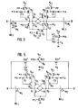
- Fig. 1 shows a major part of a dynamic memory according to a prior art.
- MOS field effect transistors (MOSTs) Q 1 and Q 2 having gates and drains cross-coupled at nodes N 1 and N 2 . and sources commonly.connected to a common node N C and a discharge MOST Q12 form a known flip-flop type sense amplifier.
- a pair of bit linesB and B are connected to the nodes N 1 and N 2 , respectively.
- a plurality of word lines WL 1 ' W L2 or the like intersect with the bit lines.
- Memory cells MC each comprised of a transfer MOST Q M and a storage capacitor C M are connected to the bit lines and word lines in a known way.
- MOSTs Q 3 , Q 4' Q5 and Q 6 and a boost capacitor C 1 form.an active pull-up circuit for the bit line B while MOSTs Q 7 , Q 8 , Q 9 and Q 10 and a boost capacitor C 2 form another active pull-up oircuit for the bit line B .
- a pulse ⁇ B changes from a low (GND) level to a high level (V cc ) so that MOST Oil is rendered conductive at T 1 .
- V cc high level
- the bit.lines B and B which have been of V cc and GND respectively change to the same intermediate .voltage V R as a reference for operating the sense amplifier.
- a pulse ⁇ p is raised to V cc at a time. T 2 . Accordingly, output ends of the boost capacitors C 1 and C 2 are charged to V cc .
- MOST Q 10 becomes conductive due to the discharged level of the bit line B and therefore the capacitor C 2 arranged for the lower,potential side bit B is discharged, while charge of the capacitor.C l is maintained. Subsequently, a pulse ⁇ A is raised at a time T 6 so that a gate potential of MOST Q 4 is raised above V cc through the capacitor and MOST Q 6 assuines a conductive state. Therefore, the power voltage V cc is applied to the higher potential side bit line B through MOSTs Q 4 and Q 5 thereby to achieve pulling-up of the bit line B to V oc in potential. While the capacitor C 2 has been discharged and MOST Q 10 has been conductive so that a gate potential cannot be raised by ⁇ A .
- MOST Q 8 remains non-conductive so that the power voltage V cc is not applied to the lower potential side bit line B .
- the potential difference between the bit lines B and B is extended to. V cc .
- the pulses ⁇ A and ⁇ S are changed to GND potential at a time T 7 to complete an access cycle.
- the pair of bit lines B and B are designed to have the same capacitance "C B ". After completion of pulling-up, a pair of bit lines B arid B prima-facially seem to become the potential V R of 1/2 V cc due to charge division expressed as:
- V R the practical .value of V R is lower than the half the power voltage.
- V R becomes about 0.43 V cc which is lower than 1/2 V cc .
- V R it is desirable to select the value of V R at a center value (1/2 V cc ) of two potentials V and GND corresponding to "1" and "0" information stored in a memory cell.
- V R is lower than 1/2 V cc
- V D1 between V R and a potential (V cc ) of a "1" storing memory cell becomes large while the potential difference V D0 between V R and a potential (GND) of a "0" storing memory cell becomes small, as shown in F ig. 2.
- V D1 between V R and a potential (V cc ) of a "1" storing memory cell becomes large while the potential difference V D0 between V R and a potential (GND) of a "0" storing memory cell becomes small, as shown in F ig. 2.
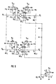
- MOST Q 20 connected between the bit line B and the common node N C and MOST Q21 connected between the bit line B and the node N C are provided for short-circuiting the bit lines B, B and the node.N C .
- a compensation capacitor C X is provided according to the invention.
- a MOST Q 23 is provided for.charging an output end of the capacitor C X to V cc in response to a pulse ⁇ pA and a MOST Q22 operatively .connects the output end of the capacitor C X to the node N C in response to the pulse ⁇ B .
- V R becomes.approximately 1/2.V.
- the capacitance of the capacitor C x is selected to have a value corresponding to the sum of the capacitance of the capacitor C 1 (C 2 ) and the capacitance of the node N C .
- the capacitor C X Prior to a time T 2 , the capacitor C X is charged to V cc through MOST Q23 in response to ⁇ PA , while the pulse ⁇ B is raised to V cc at a time T 1 so that the pair of bit lines B and B , the node N C and the capacitor C 2 are short-circuited by MOSTs Q 20 and Q 21 so that the potential on the bit lines B and B becomes a potential which is lower than 1/2 V cc similarly to the case of Fig. 1. Then, MOST Q 22 becomes conductive in response to the rise of ⁇ C to connect the output end of the capacitor C X to the short- .
- the sense amplifier and the active pull-up circuits are sequentially enabled by ⁇ S and ⁇ A at a time T 8 and a time T 9 , respectively in the same manner as in Fig. 1 to achieve an access operation.
- the bit lines B and B are accurately precharged to 1/2 V cc , and therefore the voltage difference V D1 ' between the precharge voltage V R and the potential of a "1" storing memory cell and the voltage difference V D0 ' between V R ' and the potential of a "0" storing memory cell are made equal from eath other.
- V D1 ' between the precharge voltage V R and the potential of a "1" storing memory cell
- V D0 ' between V R ' and the potential of a "0" storing memory cell
- Fig. 5 shows a second embodiment of the present invention.
- This embodiment is obtained by directly connecting the output end of the capacitor C x to the pair of bit lines B and B by MOST Q 20 , and Q 21 in place of MOSTs Q 20 to Q 22 in Fig. 3.
- MOST Q 22 and the pulse ⁇ C are obviated.
- the capacitance of the capacitor C X is determined according to the equation (3), this embodiment also provides the' same effect. Timing relations of the respective pulses in this circuit are substantially the same as those in Fig. 3.
- This.embodiment is featured in that the common nodes NC 1 to NC n of a plurality sense amplifiers for a plurality pairs of bit lines B 1 , B , to B n , B n are connected in common and MOST Q 12 ' for enabling the sense amplifiers in response to ⁇ S and MOSTs Q 2 and Q 23 and the capacitor C X ' are connected to the commonly connected nodes NC 1 to NC n , as illustrated.
- the capacitance of the capacitor C X ' is selected "n" times the sum of the capacitance C A of each capacitor C 1 , C 2 and the capacitance C S of each node (NC 1 .to NC n ), "n” being the number of the sense amplifiers.
- a pair of bit lines B and B are accurately precharged to 1/2 V cc . Therefore a dynamic memory having a high-sensitivity can be obtained.
Landscapes
- Engineering & Computer Science (AREA)
- Microelectronics & Electronic Packaging (AREA)
- Computer Hardware Design (AREA)
- Dram (AREA)
Applications Claiming Priority (2)
| Application Number | Priority Date | Filing Date | Title |
|---|---|---|---|
| JP1587785 | 1985-01-30 | ||
| JP15877/85 | 1985-01-30 |
Publications (3)
| Publication Number | Publication Date |
|---|---|
| EP0189908A2 true EP0189908A2 (de) | 1986-08-06 |
| EP0189908A3 EP0189908A3 (en) | 1990-01-10 |
| EP0189908B1 EP0189908B1 (de) | 1992-10-28 |
Family
ID=11901019
Family Applications (1)
| Application Number | Title | Priority Date | Filing Date |
|---|---|---|---|
| EP86101143A Expired EP0189908B1 (de) | 1985-01-30 | 1986-01-29 | Dynamischer Speicher mit einer Anordnung für Bitzeilenvorladung |
Country Status (4)
| Country | Link |
|---|---|
| US (1) | US4733373A (de) |
| EP (1) | EP0189908B1 (de) |
| JP (1) | JPH0793010B2 (de) |
| DE (1) | DE3687005T2 (de) |
Cited By (3)
| Publication number | Priority date | Publication date | Assignee | Title |
|---|---|---|---|---|
| EP0223621A3 (en) * | 1985-10-08 | 1990-01-31 | Fujitsu Limited | Semiconductor memory device having a circuit for compensating for discriminating voltage variations of a memory cell |
| EP0383080A3 (de) * | 1989-01-31 | 1991-06-26 | Kabushiki Kaisha Toshiba | Halbleiter-Speicher |
| EP0388176A3 (de) * | 1989-03-17 | 1993-01-07 | Matsushita Electronics Corporation | Halbleiter-Speichereinrichtung |
Families Citing this family (6)
| Publication number | Priority date | Publication date | Assignee | Title |
|---|---|---|---|---|
| JPH0810550B2 (ja) * | 1986-09-09 | 1996-01-31 | 日本電気株式会社 | バツフア回路 |
| JP3183699B2 (ja) * | 1992-03-13 | 2001-07-09 | 沖電気工業株式会社 | 半導体記憶装置 |
| KR102161737B1 (ko) * | 2013-12-02 | 2020-10-05 | 삼성전자주식회사 | 반도체 메모리 장치의 비트라인 센싱 방법 |
| US9378780B1 (en) * | 2015-06-16 | 2016-06-28 | National Tsing Hua University | Sense amplifier |
| CN112102863B (zh) * | 2020-09-07 | 2023-04-25 | 海光信息技术股份有限公司 | 静态随机存取存储器控制电路、方法、存储器和处理器 |
| EP4471773B1 (de) * | 2023-05-31 | 2025-12-10 | STMicroelectronics International N.V. | Speichervorrichtung mit leseverstärkerschaltung und betriebsverfahren |
Family Cites Families (8)
| Publication number | Priority date | Publication date | Assignee | Title |
|---|---|---|---|---|
| JPS52152129A (en) * | 1976-06-14 | 1977-12-17 | Nippon Telegr & Teleph Corp <Ntt> | Memory signal detection-amplification unit |
| JPS6011393B2 (ja) * | 1977-06-21 | 1985-03-25 | 日本電気株式会社 | 感知増幅器 |
| US4397003A (en) * | 1980-06-02 | 1983-08-02 | Mostek Corporation | Dynamic random access memory |
| JPS59132492A (ja) * | 1982-12-22 | 1984-07-30 | Fujitsu Ltd | 半導体記憶装置 |
| JPS59188887A (ja) * | 1983-04-11 | 1984-10-26 | Nec Corp | ダイナミツクメモリの駆動方法 |
| US4608670A (en) * | 1984-08-02 | 1986-08-26 | Texas Instruments Incorporated | CMOS sense amplifier with N-channel sensing |
| US4627033A (en) * | 1984-08-02 | 1986-12-02 | Texas Instruments Incorporated | Sense amplifier with reduced instantaneous power |
| US4638463A (en) * | 1985-01-24 | 1987-01-20 | International Business Machines Corporation | Fast writing circuit for a soft error protected storage cell |
-
1986
- 1986-01-29 DE DE8686101143T patent/DE3687005T2/de not_active Expired - Fee Related
- 1986-01-29 EP EP86101143A patent/EP0189908B1/de not_active Expired
- 1986-01-30 US US06/824,030 patent/US4733373A/en not_active Expired - Fee Related
- 1986-01-30 JP JP61019418A patent/JPH0793010B2/ja not_active Expired - Lifetime
Cited By (3)
| Publication number | Priority date | Publication date | Assignee | Title |
|---|---|---|---|---|
| EP0223621A3 (en) * | 1985-10-08 | 1990-01-31 | Fujitsu Limited | Semiconductor memory device having a circuit for compensating for discriminating voltage variations of a memory cell |
| EP0383080A3 (de) * | 1989-01-31 | 1991-06-26 | Kabushiki Kaisha Toshiba | Halbleiter-Speicher |
| EP0388176A3 (de) * | 1989-03-17 | 1993-01-07 | Matsushita Electronics Corporation | Halbleiter-Speichereinrichtung |
Also Published As
| Publication number | Publication date |
|---|---|
| EP0189908B1 (de) | 1992-10-28 |
| JPH0793010B2 (ja) | 1995-10-09 |
| JPS6231092A (ja) | 1987-02-10 |
| DE3687005T2 (de) | 1993-03-25 |
| US4733373A (en) | 1988-03-22 |
| EP0189908A3 (en) | 1990-01-10 |
| DE3687005D1 (de) | 1992-12-03 |
Similar Documents
| Publication | Publication Date | Title |
|---|---|---|
| US4070590A (en) | Sensing circuit for memory cells | |
| US4475178A (en) | Semiconductor regeneration/precharge device | |
| US4943952A (en) | Semiconductor memory circuit with improved bit lane precharge circuit | |
| US6266287B1 (en) | Variable equilibrate voltage circuit for paired digit lines | |
| US4397003A (en) | Dynamic random access memory | |
| US5184324A (en) | Dynamic semiconductor multi-value memory device | |
| US5138578A (en) | Semiconductor memory circuit having an improved restoring scheme | |
| EP0124868B1 (de) | Halbleiterspeicher | |
| EP0474238A2 (de) | Halbleiterspeicherschaltung | |
| US6304505B1 (en) | Differential correlated double sampling DRAM sense amplifier | |
| JPS60239993A (ja) | ダイナミツク型半導体記憶装置 | |
| US5029137A (en) | Semiconductor memory device with tandem sense amplifier units | |
| JPH06215564A (ja) | 半導体記憶装置 | |
| EP0089720B1 (de) | RAM Speicher mit einem einzigen Transistor und Kondensator | |
| JP3399787B2 (ja) | 半導体記憶装置 | |
| EP0189908A2 (de) | Dynamischer Speicher mit einer Anordnung für Bitzeilenvorladung | |
| EP0073677B1 (de) | MIS Transistorschaltung mit einer Spannungshalteschaltung | |
| EP0373672B1 (de) | Halbleiterspeicherschaltung mit einer verbesserten Wiederherstellungssteuerschaltung | |
| EP0048464A2 (de) | Halbleiterspeicheranordnung | |
| US4633443A (en) | Dynamic read/write memory circuits with equal-sized dummy and storage capacitors | |
| US4409672A (en) | Dynamic semiconductor memory device | |
| US4858193A (en) | Preamplification method and apparatus for dram sense amplifiers | |
| US4547868A (en) | Dummy-cell circuitry for dynamic read/write memory | |
| US4404661A (en) | Semiconductor memory circuit | |
| US4926381A (en) | Semiconductor memory circuit with sensing arrangement free from malfunction |
Legal Events
| Date | Code | Title | Description |
|---|---|---|---|
| PUAI | Public reference made under article 153(3) epc to a published international application that has entered the european phase |
Free format text: ORIGINAL CODE: 0009012 |
|
| 17P | Request for examination filed |
Effective date: 19860129 |
|
| AK | Designated contracting states |
Kind code of ref document: A2 Designated state(s): DE FR GB |
|
| PUAL | Search report despatched |
Free format text: ORIGINAL CODE: 0009013 |
|
| AK | Designated contracting states |
Kind code of ref document: A3 Designated state(s): DE FR GB |
|
| 17Q | First examination report despatched |
Effective date: 19910412 |
|
| GRAA | (expected) grant |
Free format text: ORIGINAL CODE: 0009210 |
|
| AK | Designated contracting states |
Kind code of ref document: B1 Designated state(s): DE FR GB |
|
| REF | Corresponds to: |
Ref document number: 3687005 Country of ref document: DE Date of ref document: 19921203 |
|
| ET | Fr: translation filed | ||
| PLBE | No opposition filed within time limit |
Free format text: ORIGINAL CODE: 0009261 |
|
| STAA | Information on the status of an ep patent application or granted ep patent |
Free format text: STATUS: NO OPPOSITION FILED WITHIN TIME LIMIT |
|
| 26N | No opposition filed | ||
| PGFP | Annual fee paid to national office [announced via postgrant information from national office to epo] |
Ref country code: DE Payment date: 19940323 Year of fee payment: 9 |
|
| PGFP | Annual fee paid to national office [announced via postgrant information from national office to epo] |
Ref country code: FR Payment date: 19950117 Year of fee payment: 10 |
|
| PGFP | Annual fee paid to national office [announced via postgrant information from national office to epo] |
Ref country code: GB Payment date: 19950120 Year of fee payment: 10 |
|
| PG25 | Lapsed in a contracting state [announced via postgrant information from national office to epo] |
Ref country code: DE Effective date: 19951003 |
|
| PG25 | Lapsed in a contracting state [announced via postgrant information from national office to epo] |
Ref country code: GB Effective date: 19960129 |
|
| GBPC | Gb: european patent ceased through non-payment of renewal fee |
Effective date: 19960129 |
|
| PG25 | Lapsed in a contracting state [announced via postgrant information from national office to epo] |
Ref country code: FR Effective date: 19960930 |
|
| REG | Reference to a national code |
Ref country code: FR Ref legal event code: ST |