EP0180661A1 - Récepteur de télévision avec reproduction d'un signal vidéo interlacé libre de scintillement - Google Patents
Récepteur de télévision avec reproduction d'un signal vidéo interlacé libre de scintillement Download PDFInfo
- Publication number
- EP0180661A1 EP0180661A1 EP84113457A EP84113457A EP0180661A1 EP 0180661 A1 EP0180661 A1 EP 0180661A1 EP 84113457 A EP84113457 A EP 84113457A EP 84113457 A EP84113457 A EP 84113457A EP 0180661 A1 EP0180661 A1 EP 0180661A1
- Authority
- EP
- European Patent Office
- Prior art keywords
- word
- line
- memory area
- memory
- digital
- Prior art date
- Legal status (The legal status is an assumption and is not a legal conclusion. Google has not performed a legal analysis and makes no representation as to the accuracy of the status listed.)
- Granted
Links
- 230000015654 memory Effects 0.000 claims abstract description 135
- 230000033001 locomotion Effects 0.000 claims abstract description 30
- 230000002457 bidirectional effect Effects 0.000 claims abstract description 12
- 230000003111 delayed effect Effects 0.000 claims description 10
- 238000000034 method Methods 0.000 claims description 10
- 238000006243 chemical reaction Methods 0.000 claims description 9
- 230000002123 temporal effect Effects 0.000 description 3
- 206010038743 Restlessness Diseases 0.000 description 2
- 238000010586 diagram Methods 0.000 description 2
- 238000009826 distribution Methods 0.000 description 2
- 238000003860 storage Methods 0.000 description 2
- 230000005540 biological transmission Effects 0.000 description 1
- 239000013078 crystal Substances 0.000 description 1
- 238000001514 detection method Methods 0.000 description 1
- 230000000694 effects Effects 0.000 description 1
- 230000008030 elimination Effects 0.000 description 1
- 238000003379 elimination reaction Methods 0.000 description 1
- 230000005669 field effect Effects 0.000 description 1
- 230000010354 integration Effects 0.000 description 1
- 230000009191 jumping Effects 0.000 description 1
- 238000004519 manufacturing process Methods 0.000 description 1
- 238000013507 mapping Methods 0.000 description 1
- 230000009291 secondary effect Effects 0.000 description 1
- 230000035945 sensitivity Effects 0.000 description 1
Images


Classifications
-
- H—ELECTRICITY
- H04—ELECTRIC COMMUNICATION TECHNIQUE
- H04N—PICTORIAL COMMUNICATION, e.g. TELEVISION
- H04N7/00—Television systems
- H04N7/01—Conversion of standards, e.g. involving analogue television standards or digital television standards processed at pixel level
- H04N7/0127—Conversion of standards, e.g. involving analogue television standards or digital television standards processed at pixel level by changing the field or frame frequency of the incoming video signal, e.g. frame rate converter
- H04N7/0132—Conversion of standards, e.g. involving analogue television standards or digital television standards processed at pixel level by changing the field or frame frequency of the incoming video signal, e.g. frame rate converter the field or frame frequency of the incoming video signal being multiplied by a positive integer, e.g. for flicker reduction
-
- Y—GENERAL TAGGING OF NEW TECHNOLOGICAL DEVELOPMENTS; GENERAL TAGGING OF CROSS-SECTIONAL TECHNOLOGIES SPANNING OVER SEVERAL SECTIONS OF THE IPC; TECHNICAL SUBJECTS COVERED BY FORMER USPC CROSS-REFERENCE ART COLLECTIONS [XRACs] AND DIGESTS
- Y10—TECHNICAL SUBJECTS COVERED BY FORMER USPC
- Y10S—TECHNICAL SUBJECTS COVERED BY FORMER USPC CROSS-REFERENCE ART COLLECTIONS [XRACs] AND DIGESTS
- Y10S348/00—Television
- Y10S348/91—Flicker reduction
Definitions
- the published patent application DE 32 03 978 A1 also describes an arrangement with field frequency doubling, which works with three field memories. These are interconnected by a suitable arrangement of multiple switches.
- the received digital video signal is alternately written into two field memories.
- the previous field already present in the second field memory is available for double-speed reading.
- a further signal delay is generated by means of the third field memory, so that when the switches are suitably actuated, a few successive fields are available at the outputs of the three field memories.
- this system can be used to achieve double-speed field playback as well as corresponding full-screen playback.
- the third field memory can be read and written simultaneously in certain phases of reading at twice the speed, so that it is loaded with four times the incoming data rate.
- Fig. 1 is provided corresponding to that of each H albsent H1, H2 of the transmitted and received television image from each 5 lines is alternately nested. Lines 1 ... 5 of field H1 are thus interleaved with lines 6 ... 10 of second field H2 in such a way that line sequence 1, 6; 2, 7; ... 5, 10 arises.
- Strength in F. 2 is schematically illustrates a mapping scheme for writing and the double-speed reading in and out of the envisaged in the invention, frame memory vs (F ig. 3) is shown. As indicated by the arrow t, the assignment scheme is to be understood in terms of time, ie it shows how the individual lines are written into the full-screen memory vs and read out from it in succession.
- FIG. 2a shows the "slow" (line-frequency) writing of the fields B1 and B2 of the frame B. The pixel delayed by the duration of a frame can first be read out and then rewritten by the new pixel plus the movement information.
- the full-frame memory vs consists of the three memory areas spl, sp2, sp3, each of which is assigned the first, second or third multiplexer mxl, mx2, mx3.
- Each memory area is in fact connected to each multiplexer via the first or second or third bidirectional data bus dbl, db2, db3, the data transfer on these buses (block by data) taking place only in one direction, that is, even though they are bidirectional data buses at a certain point in time, there is never a flow of data in both directions, but only in one.
- the first and second multiplexer mxl, mx2 is also located on the first and second input of the field interpolator ip via the first and second unidirectional data bus ebl, eb2.
- the two multiplexers mx1, mx2 are therefore preferably unidirectional multiplexers, while the multiplexer mx3 has to transmit data in two directions and is therefore connected via the fourth two-directional data bus db4 to the motion detector bt, at the input of which the digital video signal dv lies, while at the output of the field interpolator ip the digital flicker-free video signal fv occurs.
- the sequence control circuit cc operated on a clock oscillator, not shown, which, among other things, generates the clock signal ft required here and also other system clock signals for the individual digital subcircuits of the television receiver, controls the line-frequency writing and the read-out once or twice at twice the line frequency in or from the three memory areas of the full-screen memory vs.
- the information of a line which is hereinafter referred to briefly as "data word”, is compressed to half the line duration before writing w, which e.g. in a corresponding stage of the motion detector bt or can also take place in a stage provided for this purpose. It is thereby achieved that the temporal interleaving of the individual data words in the three memory areas sp1, sp2, sp3 to be explained with reference to FIGS. 4 to 6 is possible.
- the blocks or parts of the data words of the individual lines are not distinguished from one another with respect to the reference symbols, but rather the blocks or parts belonging to a line are designated by the number of this line.
- the first word block is an nth line, where n is an integer from the sequence 1, 4,... N / 2 and N is the number of full-screen lines or only the number of lines with image information of a full image.
- the first word part of an m-th line becomes the second in the second memory area sp2 and its second word part in the third memory area sp3 word part of a (m + 1) - t s line in the first memory district sp1 and the second part of word in the second memory district sp2 and the first word section of an (m + 2) -th row in the third memory district sp3 and the second part of word in the first memory district sp1 stored.
- sequence of three (the sequence of three therefore begins with the m or nth line), is now the data delayed by one frame time word of the corresponding m or nth line read out from the frame memory vs, cf. to 6 r the section in Fig. 4, th n-with the data word of the m- or line in the motion detector bt compared and written during the first half of the duration of the next Dreierfol g e of rows together with the motion information in those memory areas, in which the data word is delayed by one frame time, whereby this previous data word is replaced by the new one.
- the first, second and third word block of each data word of the nth line is read out together with the corresponding word part of each data word of the mth line, which, as already explained above, occurs once or twice at twice the line frequency.
- the temporal assignment of the parts originating from the individual lines of the fields is shown schematically.
- the same word blocks or word parts of the corresponding lines thus belong together, such as the line numbers 1, 6 in a column in FIGS. 4b and d; 7, 2; 2, 7 etc. show.
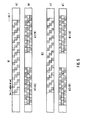
- the four Z u glovessschemata of Fig. 5 are for a different distribution of the data words, namely, each divided into three blocks word or word parts.
- the successive writing is carried out in such a way that the first word block is stored in the first memory area spl, the second word block in the second memory area sp2 and the third word block in the third memory area sp3 (FIG. 5a).
- the first word part is stored in the second memory area sp2, the second word part in the third memory area sp3 and the third word part in the third memory area sp1.
- FIGS. 5a and 5c the successive writing is carried out in such a way that the first word block is stored in the first memory area spl, the second word block in the second memory area sp2 and the third word block in the third memory area sp3 (FIG. 5a).
- the first word part is stored in the second memory area sp2, the second word part in the third memory area sp3 and the third word part
- 5b and d are, in turn, similar atenwortmaschine D in columns one above the other, which are read at double the line frequency.
- the processing is bt g ungsdetektor in BEWE and return save during the time period w corresponding to the same as the variant of the solution according to Fig. 4.
- the first word block of an (n + 2) th line in the third memory area sp3 the second word block in the first memory area sp1, the third word block in the second memory area sp2 and the fourth word block in the third memory area sp3.
- One of the integration techniques customary for digital circuits is suitable for realizing the full-frame memory and the integrated circuit ic, the technology of the integrated insulating layer field-effect transistor circuits, in particular the so-called MOS technology, being of particular interest.
- the invention can cooperate with the integrated circuits for digital signal processing in television receivers already described in the specialist literature, cf. e.g. "Electronics", August 11, 1981, pages 97 to 103.
- the aforementioned conversion of the video signal obtained in the television receiver on the analog side into a digital video signal and its further processing on the digital side can be done in the manner described above for the television receiver of the invention.
- the corresponding subcircuits are not specified in the figures of the drawing, but it is assumed that the aforementioned subcircuits provide the digital video signal dv according to FIG. 3.
Landscapes
- Engineering & Computer Science (AREA)
- Multimedia (AREA)
- Signal Processing (AREA)
- Television Systems (AREA)
Priority Applications (6)
| Application Number | Priority Date | Filing Date | Title |
|---|---|---|---|
| EP84113457A EP0180661B1 (fr) | 1984-11-08 | 1984-11-08 | Récepteur de télévision avec reproduction d'un signal vidéo interlacé libre de scintillement |
| DE8484113457T DE3482365D1 (de) | 1984-11-08 | 1984-11-08 | Fernsehempfaenger mit flimmerfreier wiedergabe eines zwischenzeilen-videosignals. |
| CN85107729.3A CN1005811B (zh) | 1984-11-08 | 1985-10-22 | 无闪烁地重现隔行扫描视频信号的电视接收机 |
| AU49086/85A AU4908685A (en) | 1984-11-08 | 1985-10-25 | Anti-flicker display using field memory read out sequence control |
| US06/794,518 US4683497A (en) | 1984-11-08 | 1985-11-04 | Television receiver for flicker-free reproduction of an interlaced video signal |
| JP60249105A JP2517547B2 (ja) | 1984-11-08 | 1985-11-08 | テレビジヨン受像機 |
Applications Claiming Priority (1)
| Application Number | Priority Date | Filing Date | Title |
|---|---|---|---|
| EP84113457A EP0180661B1 (fr) | 1984-11-08 | 1984-11-08 | Récepteur de télévision avec reproduction d'un signal vidéo interlacé libre de scintillement |
Publications (2)
| Publication Number | Publication Date |
|---|---|
| EP0180661A1 true EP0180661A1 (fr) | 1986-05-14 |
| EP0180661B1 EP0180661B1 (fr) | 1990-05-23 |
Family
ID=8192274
Family Applications (1)
| Application Number | Title | Priority Date | Filing Date |
|---|---|---|---|
| EP84113457A Expired - Lifetime EP0180661B1 (fr) | 1984-11-08 | 1984-11-08 | Récepteur de télévision avec reproduction d'un signal vidéo interlacé libre de scintillement |
Country Status (6)
| Country | Link |
|---|---|
| US (1) | US4683497A (fr) |
| EP (1) | EP0180661B1 (fr) |
| JP (1) | JP2517547B2 (fr) |
| CN (1) | CN1005811B (fr) |
| AU (1) | AU4908685A (fr) |
| DE (1) | DE3482365D1 (fr) |
Cited By (4)
| Publication number | Priority date | Publication date | Assignee | Title |
|---|---|---|---|---|
| EP0367929A2 (fr) * | 1988-11-11 | 1990-05-16 | GRUNDIG E.M.V. Elektro-Mechanische Versuchsanstalt Max Grundig holländ. Stiftung & Co. KG. | Dispositif de réduction du papillotement dans les récepteurs de télévision |
| WO1990015503A1 (fr) * | 1989-05-29 | 1990-12-13 | N.V. Philips' Gloeilampenfabrieken | Circuit pour reduire le sautillement au niveau des lignes et des contours dans des images de television |
| EP0412003A1 (fr) * | 1989-08-04 | 1991-02-06 | Laboratoire Europeen De Recherches Electroniques Avancees | Dispositif de transformation d'une information de mouvement en un signal de détection de mouvement à la fréquence trame et au nombre de lignes souhaitées pour un récepteur de télévision haute définition |
| AU675387B2 (en) * | 1994-06-07 | 1997-01-30 | Matsushita Electric Industrial Co., Ltd. | Method and apparatus for graphic processing |
Families Citing this family (15)
| Publication number | Priority date | Publication date | Assignee | Title |
|---|---|---|---|---|
| JPH0754966B2 (ja) * | 1985-12-09 | 1995-06-07 | 株式会社日立製作所 | 輪郭補正回路 |
| JPH02202195A (ja) * | 1989-01-30 | 1990-08-10 | Pioneer Electron Corp | ビデオ信号処理装置 |
| JP2520419Y2 (ja) * | 1990-12-20 | 1996-12-18 | 三菱製鋼株式会社 | 磁気抵抗効果型素子センサーの保護装置 |
| JP2520420Y2 (ja) * | 1990-12-20 | 1996-12-18 | 三菱製鋼株式会社 | 磁気抵抗効果型素子センサーの潤滑装置 |
| US5319460A (en) * | 1991-08-29 | 1994-06-07 | Canon Kabushiki Kaisha | Image signal processing device including frame memory |
| US5900856A (en) * | 1992-03-05 | 1999-05-04 | Seiko Epson Corporation | Matrix display apparatus, matrix display control apparatus, and matrix display drive apparatus |
| US5877738A (en) * | 1992-03-05 | 1999-03-02 | Seiko Epson Corporation | Liquid crystal element drive method, drive circuit, and display apparatus |
| WO1993018501A1 (fr) * | 1992-03-05 | 1993-09-16 | Seiko Epson Corporation | Procede et circuit pour exciter des elements a cristaux liquides et dispositif d'affichage |
| US5959603A (en) * | 1992-05-08 | 1999-09-28 | Seiko Epson Corporation | Liquid crystal element drive method, drive circuit, and display apparatus |
| JP3255323B2 (ja) * | 1994-01-21 | 2002-02-12 | ブラザー工業株式会社 | 画像処理装置 |
| EP1280130A3 (fr) | 1994-11-17 | 2003-03-05 | Seiko Epson Corporation | Dispositif d'affichage et appareil électronique |
| JP3548718B2 (ja) | 1998-08-06 | 2004-07-28 | インフィネオン テクノロジース アクチエンゲゼルシャフト | ビデオ画像の画像ブロックへのランダムアクセス方法 |
| JP2001258836A (ja) * | 2000-03-16 | 2001-09-25 | Fuji Photo Optical Co Ltd | 電子内視鏡装置 |
| US7397503B2 (en) * | 2003-07-28 | 2008-07-08 | Micron Technology, Inc. | Systems and methods for reducing artifacts caused by illuminant flicker |
| US7430018B1 (en) | 2008-03-24 | 2008-09-30 | International Business Machines Corporation | Timesharing of a display screen |
Citations (1)
| Publication number | Priority date | Publication date | Assignee | Title |
|---|---|---|---|---|
| EP0070465A1 (fr) * | 1981-07-21 | 1983-01-26 | International Standard Electric Corporation | Méthode et dispositif pour élever la fréquence d'images |
Family Cites Families (7)
| Publication number | Priority date | Publication date | Assignee | Title |
|---|---|---|---|---|
| NL7706512A (nl) * | 1977-06-14 | 1978-12-18 | Philips Nv | Lijnentalomzetschakeling. |
| US4272787A (en) * | 1978-09-07 | 1981-06-09 | Micro Consultants Limited | T.V. Picture freeze system |
| DE2938349C2 (de) * | 1979-09-21 | 1983-05-26 | Aeg-Telefunken Ag, 1000 Berlin Und 6000 Frankfurt | Schaltungsanordnung zur kompatiblen Auflösungserhöhung bei Fernsehsystemen |
| US4400719A (en) * | 1981-09-08 | 1983-08-23 | Rca Corporation | Television display system with reduced line-scan artifacts |
| US4455572A (en) * | 1982-01-15 | 1984-06-19 | The United States Of America As Represented By The Secretary Of The Navy | Flicker free stretched grams |
| US4415931A (en) * | 1982-03-18 | 1983-11-15 | Rca Corporation | Television display with doubled horizontal lines |
| US4598309A (en) * | 1984-05-29 | 1986-07-01 | Rca Corporation | Television receiver that includes a frame store using non-interlaced scanning format with motion compensation |
-
1984
- 1984-11-08 DE DE8484113457T patent/DE3482365D1/de not_active Expired - Fee Related
- 1984-11-08 EP EP84113457A patent/EP0180661B1/fr not_active Expired - Lifetime
-
1985
- 1985-10-22 CN CN85107729.3A patent/CN1005811B/zh not_active Expired
- 1985-10-25 AU AU49086/85A patent/AU4908685A/en not_active Abandoned
- 1985-11-04 US US06/794,518 patent/US4683497A/en not_active Expired - Fee Related
- 1985-11-08 JP JP60249105A patent/JP2517547B2/ja not_active Expired - Lifetime
Patent Citations (1)
| Publication number | Priority date | Publication date | Assignee | Title |
|---|---|---|---|---|
| EP0070465A1 (fr) * | 1981-07-21 | 1983-01-26 | International Standard Electric Corporation | Méthode et dispositif pour élever la fréquence d'images |
Non-Patent Citations (1)
| Title |
|---|
| FERNSEH- UND KINO-TECHNIK, 38. Jahrgang, Nr. 6, Juni 1984, Seiten 231-238, Berlin, DE; H. SCHÖNFELDER: "Verbesserung der PAL-Bildqualität durch digitale Interframetechnik" * |
Cited By (5)
| Publication number | Priority date | Publication date | Assignee | Title |
|---|---|---|---|---|
| EP0367929A2 (fr) * | 1988-11-11 | 1990-05-16 | GRUNDIG E.M.V. Elektro-Mechanische Versuchsanstalt Max Grundig holländ. Stiftung & Co. KG. | Dispositif de réduction du papillotement dans les récepteurs de télévision |
| EP0367929A3 (fr) * | 1988-11-11 | 1991-11-21 | GRUNDIG E.M.V. Elektro-Mechanische Versuchsanstalt Max Grundig holländ. Stiftung & Co. KG. | Dispositif de réduction du papillotement dans les récepteurs de télévision |
| WO1990015503A1 (fr) * | 1989-05-29 | 1990-12-13 | N.V. Philips' Gloeilampenfabrieken | Circuit pour reduire le sautillement au niveau des lignes et des contours dans des images de television |
| EP0412003A1 (fr) * | 1989-08-04 | 1991-02-06 | Laboratoire Europeen De Recherches Electroniques Avancees | Dispositif de transformation d'une information de mouvement en un signal de détection de mouvement à la fréquence trame et au nombre de lignes souhaitées pour un récepteur de télévision haute définition |
| AU675387B2 (en) * | 1994-06-07 | 1997-01-30 | Matsushita Electric Industrial Co., Ltd. | Method and apparatus for graphic processing |
Also Published As
| Publication number | Publication date |
|---|---|
| AU4908685A (en) | 1986-05-15 |
| JP2517547B2 (ja) | 1996-07-24 |
| CN1005811B (zh) | 1989-11-15 |
| DE3482365D1 (de) | 1990-06-28 |
| US4683497A (en) | 1987-07-28 |
| EP0180661B1 (fr) | 1990-05-23 |
| CN85107729A (zh) | 1986-06-10 |
| JPS61117989A (ja) | 1986-06-05 |
Similar Documents
| Publication | Publication Date | Title |
|---|---|---|
| EP0180661B1 (fr) | Récepteur de télévision avec reproduction d'un signal vidéo interlacé libre de scintillement | |
| DE3878504T2 (de) | Vorrichtung zur verarbeitung eines videosignals. | |
| DE69227821T2 (de) | Fernsehsystem mit einem Speicher mit mehrfachem seriellen Zugriff | |
| DE4012520C2 (de) | Fernsehanordnung mit Einrichtungen zur Verarbeitung einer Mehrbilddarstellung | |
| DE2824561C2 (fr) | ||
| DE2946359C2 (fr) | ||
| DE2919493C2 (de) | Schaltungsanordnung zur Erzeugung einer digitalen Video-Mischsignalfolge, die ein aus mehreren Fernsehbildern zusammengesetztes Bild darstellt | |
| DE69126909T2 (de) | Videosignalanzeigevorrichtung | |
| DE3220958A1 (de) | Fluessigkeitskristall-matrixanzeigeanordnung | |
| DE2413839C3 (de) | Fernsehempfänger mit einer Einrichtung zur gleichzeitigen Wiedergabe mehrerer Programme | |
| DE3415348A1 (de) | Anordnung zum herstellen einer photo-, dia- bzw. filmabbildung eines fernsehbildes | |
| DE69012246T2 (de) | Anzeigevorrichtung. | |
| DE2919157C2 (de) | Trickvorrichtung zur graduellen Bildverschiebung auf elektronischem Wege | |
| DE1774682B2 (de) | Einrichtung zur sichtbaren Datenwiedergabe | |
| DE69123478T2 (de) | Elektronische Zoomeinrichtung | |
| DE2237269B2 (de) | Verfahren zur Umänderung eines handelsüblichen Fernsehempfängers in ein Datensichtgerät sowie ein entsprechend abgewandeltes Fernsehgerät | |
| DE3883577T2 (de) | Bildaufnahmegerät. | |
| EP0298362A1 (fr) | Méthode et dispositif d'agrandissement d'une portion d'image de télévision | |
| DE2510542A1 (de) | Digitale bildwiedergabevorrichtung mit mehreren bildschirmen | |
| DE2855152C2 (fr) | ||
| DE2803101C2 (de) | Verfahren und Schaltungsanordnung zur Erzeugung eines Monitorbildes als Teilausschnitt eines Großbildes | |
| DE4027180C2 (de) | Vorrichtung zum Erzeugen von Vertikalrolladressen | |
| DE69106794T2 (de) | Videosignalverarbeitungsverfahren. | |
| EP0318760A2 (fr) | Récepteur de télévision avec un dispositif de suppression des perturbations de scintillement | |
| EP0298394A2 (fr) | Méthode et dispositif de réduction de la visibilité de la structure de lignes d'une image de télévision |
Legal Events
| Date | Code | Title | Description |
|---|---|---|---|
| PUAI | Public reference made under article 153(3) epc to a published international application that has entered the european phase |
Free format text: ORIGINAL CODE: 0009012 |
|
| AK | Designated contracting states |
Kind code of ref document: A1 Designated state(s): DE FR GB IT NL |
|
| 17P | Request for examination filed |
Effective date: 19861108 |
|
| 17Q | First examination report despatched |
Effective date: 19881027 |
|
| GRAA | (expected) grant |
Free format text: ORIGINAL CODE: 0009210 |
|
| AK | Designated contracting states |
Kind code of ref document: B1 Designated state(s): DE FR GB IT NL |
|
| REF | Corresponds to: |
Ref document number: 3482365 Country of ref document: DE Date of ref document: 19900628 |
|
| ET | Fr: translation filed | ||
| ITF | It: translation for a ep patent filed | ||
| GBT | Gb: translation of ep patent filed (gb section 77(6)(a)/1977) | ||
| PLBE | No opposition filed within time limit |
Free format text: ORIGINAL CODE: 0009261 |
|
| STAA | Information on the status of an ep patent application or granted ep patent |
Free format text: STATUS: NO OPPOSITION FILED WITHIN TIME LIMIT |
|
| 26N | No opposition filed | ||
| ITTA | It: last paid annual fee | ||
| PGFP | Annual fee paid to national office [announced via postgrant information from national office to epo] |
Ref country code: FR Payment date: 19971021 Year of fee payment: 14 |
|
| PGFP | Annual fee paid to national office [announced via postgrant information from national office to epo] |
Ref country code: GB Payment date: 19971027 Year of fee payment: 14 |
|
| PGFP | Annual fee paid to national office [announced via postgrant information from national office to epo] |
Ref country code: NL Payment date: 19971031 Year of fee payment: 14 |
|
| PGFP | Annual fee paid to national office [announced via postgrant information from national office to epo] |
Ref country code: DE Payment date: 19971121 Year of fee payment: 14 |
|
| PG25 | Lapsed in a contracting state [announced via postgrant information from national office to epo] |
Ref country code: GB Free format text: LAPSE BECAUSE OF NON-PAYMENT OF DUE FEES Effective date: 19981108 |
|
| PG25 | Lapsed in a contracting state [announced via postgrant information from national office to epo] |
Ref country code: NL Free format text: LAPSE BECAUSE OF NON-PAYMENT OF DUE FEES Effective date: 19990601 |
|
| GBPC | Gb: european patent ceased through non-payment of renewal fee |
Effective date: 19981108 |
|
| PG25 | Lapsed in a contracting state [announced via postgrant information from national office to epo] |
Ref country code: FR Free format text: LAPSE BECAUSE OF NON-PAYMENT OF DUE FEES Effective date: 19990730 |
|
| NLV4 | Nl: lapsed or anulled due to non-payment of the annual fee |
Effective date: 19990601 |
|
| REG | Reference to a national code |
Ref country code: FR Ref legal event code: ST |
|
| PG25 | Lapsed in a contracting state [announced via postgrant information from national office to epo] |
Ref country code: DE Free format text: LAPSE BECAUSE OF NON-PAYMENT OF DUE FEES Effective date: 19990901 |