EP0168220A2 - Verfahren und Einrichtung zur Umwandlung eines Analogsignals in ein Digitalsignal mittels einer Übertastungstechnik - Google Patents
Verfahren und Einrichtung zur Umwandlung eines Analogsignals in ein Digitalsignal mittels einer Übertastungstechnik Download PDFInfo
- Publication number
- EP0168220A2 EP0168220A2 EP85304798A EP85304798A EP0168220A2 EP 0168220 A2 EP0168220 A2 EP 0168220A2 EP 85304798 A EP85304798 A EP 85304798A EP 85304798 A EP85304798 A EP 85304798A EP 0168220 A2 EP0168220 A2 EP 0168220A2
- Authority
- EP
- European Patent Office
- Prior art keywords
- signal
- frequency
- output
- integrator
- converting
- Prior art date
- Legal status (The legal status is an assumption and is not a legal conclusion. Google has not performed a legal analysis and makes no representation as to the accuracy of the status listed.)
- Granted
Links
- 238000000034 method Methods 0.000 title claims description 13
- 238000005070 sampling Methods 0.000 claims abstract description 46
- 238000006243 chemical reaction Methods 0.000 claims description 4
- 230000015654 memory Effects 0.000 claims description 4
- 230000010354 integration Effects 0.000 claims description 2
- 238000001914 filtration Methods 0.000 abstract 1
- 230000006870 function Effects 0.000 description 9
- 238000007792 addition Methods 0.000 description 7
- 238000010586 diagram Methods 0.000 description 5
- 230000009467 reduction Effects 0.000 description 5
- 230000004044 response Effects 0.000 description 5
- 238000013139 quantization Methods 0.000 description 3
- 238000004519 manufacturing process Methods 0.000 description 2
- 238000007493 shaping process Methods 0.000 description 2
- 108010076504 Protein Sorting Signals Proteins 0.000 description 1
- 238000009825 accumulation Methods 0.000 description 1
- 230000008901 benefit Effects 0.000 description 1
- 238000004364 calculation method Methods 0.000 description 1
- 230000008859 change Effects 0.000 description 1
- 238000010276 construction Methods 0.000 description 1
- 230000007423 decrease Effects 0.000 description 1
- 230000003247 decreasing effect Effects 0.000 description 1
- 230000003111 delayed effect Effects 0.000 description 1
- 230000000694 effects Effects 0.000 description 1
- 238000010348 incorporation Methods 0.000 description 1
- 230000008569 process Effects 0.000 description 1
- 230000002441 reversible effect Effects 0.000 description 1
- 238000001228 spectrum Methods 0.000 description 1
Images


Classifications
-
- H—ELECTRICITY
- H03—ELECTRONIC CIRCUITRY
- H03M—CODING; DECODING; CODE CONVERSION IN GENERAL
- H03M3/00—Conversion of analogue values to or from differential modulation
- H03M3/30—Delta-sigma modulation
- H03M3/458—Analogue/digital converters using delta-sigma modulation as an intermediate step
- H03M3/462—Details relating to the decimation process
-
- H—ELECTRICITY
- H03—ELECTRONIC CIRCUITRY
- H03M—CODING; DECODING; CODE CONVERSION IN GENERAL
- H03M3/00—Conversion of analogue values to or from differential modulation
- H03M3/30—Delta-sigma modulation
- H03M3/39—Structural details of delta-sigma modulators, e.g. incremental delta-sigma modulators
- H03M3/412—Structural details of delta-sigma modulators, e.g. incremental delta-sigma modulators characterised by the number of quantisers and their type and resolution
- H03M3/422—Structural details of delta-sigma modulators, e.g. incremental delta-sigma modulators characterised by the number of quantisers and their type and resolution having one quantiser only
- H03M3/43—Structural details of delta-sigma modulators, e.g. incremental delta-sigma modulators characterised by the number of quantisers and their type and resolution having one quantiser only the quantiser being a single bit one
-
- H—ELECTRICITY
- H03—ELECTRONIC CIRCUITRY
- H03M—CODING; DECODING; CODE CONVERSION IN GENERAL
- H03M3/00—Conversion of analogue values to or from differential modulation
- H03M3/30—Delta-sigma modulation
- H03M3/39—Structural details of delta-sigma modulators, e.g. incremental delta-sigma modulators
- H03M3/436—Structural details of delta-sigma modulators, e.g. incremental delta-sigma modulators characterised by the order of the loop filter, e.g. error feedback type
- H03M3/456—Structural details of delta-sigma modulators, e.g. incremental delta-sigma modulators characterised by the order of the loop filter, e.g. error feedback type the modulator having a first order loop filter in the feedforward path
Definitions
- This invention relates to an oversampled analog-to-digital (A/D) converting method and apparatus capable of achieving precise coding.
- Oversampled coders sample an analog signal at a higher frequency than the Nyquist frequency, quantize the sampled signal, and perform the bandlimitation and reduction of the sampling frequency to produce a coded output.
- oversampled coder For details of the oversampled coder, reference is made to an article by Stuart K. Tewksbury et al., entitled “Oversampled, r Linear Predictive and Noise-Shaping Coders of'Oder N > 1", published in the IEEE Transactions On Circuits And Systems, Vol. CAS-25, No. 7, July issue, 1978, pp. 436 - 447. Since the above-mentioned oversampled coder may be composed of only digital circuits with exception of a low resolution digital-to-analog (D/A) converter and an integrator, the coder is suitable for a large scale integration circuit (LSI).
- D/A digital-to-analog
- an object of the invention to provide a method and apparatus for A/D conversion using an oversampling technique to achieve high precision linear coding.
- an oversampled A/D converting method comprising the steps of: oversampling an input analog signal at a first frequency higher than the Nyquist frequency to produce a sampled signal; subtracting a local decoded signal from the sampled signal; quantizing the subtracted signal into a quantized binary signal; generating said local decoded signal by integrating the quantized binary signal; converting the quantized binary signal having the first frequency into a frequency-reduced signal having a second frequency; and integrating the frequency-reduced signal at the second frequency to produce a converted digital signal.
- an oversampled A/D converter comprising: means for sampling an input analog signal at a first frequency higher than the Nyquist frequency to produce a sampled signal; a subtracter for subtracting a local decoded signal from the sampled signal: a quantizer for quantizing the output of the subtracter to produce a quantized binary signal; means for integrating the quantized binary signal to generate the local decoded signal; a converting means for converting the quantized binary signal having the first frequency into a frequency-reduced signal having a second frequency; and an integrator for integrating the frequency-reduced signal at the second frequency to produce a converted digital signal.
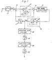
- a prior art oversampled A/D converter (referred.to as a oversampled coder) will be described with reference to Fig. 1 and Figs. 2A to 2F.
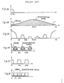
- an input analog signal applied to an input terminal 1 is assumed to have a frequency band of about f B (Hz) as shown in Fig. 2A.
- the input signal is converted into a sampled signal by a sampling switch 11 which operates at a higher sampling frequency f H than the Niquist sampling frequency, 2f B .
- a subtracter 12 subtracts a local decoded analog signal from the sampled signal to produce an error signal.
- the error signal is integrated by a noise-shaping integrator 13 to produce an integrated signal.
- Another subtracter 14 subtracts the local decoded signal from the integrated signal to supply the difference to a two level quantizer 15.
- the quantizer 15 discriminates a sign of the output of the subtracter 14 and produces + ⁇ or - ⁇ based on the discriminated positive or negative sign.
- the integrator l3 or 16 can be realized with an adder 131 or 161 and a delay circuit 132 or 162 having one sample delay.
- the sampling frequency f H is reduced to the sampling frequency f s through the intermediate sampling frequency f M .
- f M is defined as f H > f M > f s
- a digital FIR filter 18 is used to eliminate the quantization noise around a frequency integral multiple of the frequency fM prior to the sampling frequency reduction.
- the filter 18 is preferred to have the characteristic shown in Fig. 2C.
- the output of the filter 18 is resampled at the frequency f M by the sampling switch 19, the spectrum repeated at the frequency f m is obtained as shown in Fig. 2 D .
- a digital IIR filter 20 is a low-pass filter with the frequency band about f B operable at the sampling frequency f m and has the frequency characteristic shown in Fig. 2E.
- the filter 20 is combined with the filter 18 so that the inband frequency characteristic is flat. By passing through the filter 20, the quantization noise and the frequency components of the less than f M - f B (Hz) are suppressed sufficiently.
- the output of the filter 20 is then resampled by the sampling switch 21 to produce the signal with the sampling frequency f s (Fig. 2F).
- the predictive integrator 16 and filter 18 perform a high-speed operation.
- the integrator 16 which merely accumulates the output ( ⁇ ) of the quantizer 15, may consist of an up-down counter or a reversible counter.
- the invention solves the above-mentioned problems by supplying a binary signal to the digital FIR filter, thereby making the multiplication required in the digital FIR filter unnecessary.
- W(z) represents the z-transform of the output signal of the quantizer 15
- W(z) is expressed as follows:
- X(z) For obtaining X(z) from the equation, it is necessary to multiply X(z) by 1/(1 - z -1 ) in the process of reducing the sampling frequency.
- the operation of 1/(1 - z -1 ) is transformed as follows:
- the numerator on the right side of the equation (1) indicates a polynomial in respect to z -1 and a transfer function of an M-tap digital FIR filter operable at the sampling frequency f H .
- the denominator on the right side represents a polynomial as to z -M
- the numerator on the right side may be incorporated with the transfer function of the filter 18 to develop a single digital FIR filter.
- the number of taps of the filter 18 is (L + 1)
- the incorporation of the filter 18 with the numerator of the right term of equation (1) corresponding to the M-tap filter gives a synthetic digital FIR filter having (M + L) taps.
- the output y(n) is calculated at intervals of M: y(0), y(M), y(2M), ...., and y(mM).
- mM M + L
- both y(0) and y(mM) are calculated by the same hardware.
- the number of input samples necessary to yield y(0) is M + L, and they are x(-M - L + 1), x(-M - L + 2), ...., x(-1), and x(0), respectively.
- input samples necessary to yield y(mM) are x(l), x(2), ...., and x(M + L), the number of samples being M + L.
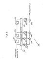
- Fig. 3 shows an embodiment of the invention in which reference numerals 1, 11, 12, 13, 14, 15, 16, 17, 20, 21, 131, 132, 161, and 162 designates components or elements corresponding to or having the same function as those designated by the same reference numerals in Fig. 1.
- the embodiment comprises a sampling frequencing converter 22 for converting the quantized binary signal having the sampling frequency f H given from the quantizer 15 into a frequency reduced signal having a sampling frequency f M , and an integrator for integrating the frequency reduced signal at the frequency f M .
- a sampling switch 222 takes out the (J + 1) bits from the delay circuits, in response to the sampling frequency f M supplied to a terminal 220, to produce a binary signal having the frequency f M .
- Adders 224 1 , 2242, ...., and 224 J summate outputs of all the coefficient circuits. It follows that the amount of operation necessary for the sampling frequency change is only J-times additions (subtractions) per 1/f M (seconds), thereby making the multiplication of the coefficients unnecessary. Also, each delay circuit made up of one bit flip flop contributes to achieving a remarkably simplified circuit structure.
- the integrator 23 comprises an adder 231, a delay circuit 232 having delay of 1/f M , and a multiplier 233 and executes the operation of 1/(1 - z -M ) in equation 1.
- the multiplier 233 performs the multiplication of a given input by " ⁇ " to bring the transfer function of the integrator 23 into 1/(1 - ⁇ z -M ).
- ⁇ the inputs signal given to the digital filter 20 is equal in the structures of Figs. 1 and 3.
- the value of ⁇ is preferred to be a little smaller than 1, because the value of ⁇ smaller than 1 reduces influence due to the initial value of the delay circuit 232 with passage of time.
- the local decoded signal given from the integrator 16 is delayed by one sample in delay circuits 81 1 , 81 2 , ...., and 81 M .
- the signals taken out of the respective delay circuits are multiplied by filter coefficients h 0 , h 1 , ...., and h L in multipliers 82 0 , 82 1 , ...., and 82 L .
- the outputs of the multipliers are summed by adders 83 1 , 83 2 , ...., and 83 L .
- the summed result is sent to the sampling switch 19.
- the filter coefficients h 0 , h 1 , ...., and h L are derived from an impulse response of this filter, and Z-transform of the impulse response and the frequency characteristic are expressed as:
- Multipliers 90 0 , 91 1 , and 91 2 , a subtracter 92 1 , an adder 92 2 and delay circuits 93 1 and 93 2 execute the operation of 1/(1 + b 11 z -M + b 21 z -2M ) in the system function H(z M ). Meanwhile, the operation of 1/(1 + a 11 z -M + a 21 z -2M ) is executed by multipliers 91 3 , 91 4 and adders 92 3 , 92 4 .
- the converter 22 comprises a counter 221, read only memories (ROM's) 222 1 , 222 2 and 2223, addition/ subtraction units (ASU's) 223 1 , 223 2 and 22-3 3 , registers 225 1 , 225 2 and 225 3 for delaying by one sampling time.
- a clock pulse at f H (bits/second) (Fig. 8A) applied to a terminal 220 is subjected to (M + L) frequency division by a counter 221.
- Fig. 8B shows contents of the counter 221: 0, 1, 2, ...., and 17 when (M + L) is 18.
- the ROM's 222 1 , 222 2 and 223 3 are addressed by the outputs of the counter 221 to produce filter coefficients h 17 , h 16 , h 15 , ...., and h 0 .
- the output of the ROM 222 i is added to or subtracted from the output of the register 224 i (Figs. 8F to 8H). As shown in Figs. 8C to 8H, when the ROM 222 1 produces the coefficient h 17 , the output of register 224 i is always "0". Whether the ASU's should perform addition or subtraction depends on the quantized output ⁇ from the quantizer 15. In the circuit shown in Fig. 7, the addition is represented by + ⁇ , while the subtraction, by - ⁇ . The outout of the. ASU 223 i is applied to the register 224 i through a switch 225 i . Figs.
- a ROM 222 0 is addressed by the content (Fig. 10) of a counter (CT) 221 0 which is obtained by frequency-dividing the clock pulse having f H (bit/second) in (M + L) (Fig. 10A).
- the ROM 221 0 receives an enabling signal given at a terminal 232, obtained by frequency dividing the clock of 3 x f H (bits/second) in three. Accordingly, the ROM 222 0 produces a filter coefficient h k changing at every ( 3 x f H ) -1 seconds (Fig. 10F). This is equivalent to the time division multiplex of the outputs of the ROM's 222 1 , 222 2 and 222 3 in Fig. 7.
- the required capacity of the ROM 222 0 is 3 x (M + L) words, which is equal to the summation of the capacities of the ROM's 222 1 , 222 2 and 222 3 .
- This also means that three ROM's 222 1 , 222 2 and 222 3 can be substituted by a single ROM, which leads to the simplification of the circuit.
- the same effect can be achieved by setting the capacity of the ROM 222 0 to (M + L) words, providing three address generator, and time-division multiplexing the three address signals.
- An ASU 223 0 performs addition or subtraction between the outputs of the ROM 222 0 and a switch 225 0 (Fig. 10G).
- the quantized signal (Fig.
- the signal stored in the register 223 i is supplied to a switch 225 0 through a gate 227 i .
- the gate 227 1 passes the output of the register 223 i in response to "1" of the timing pulse (1), (2) or (3) to time-division multiplex the output of the register 226 i .
- the switch 225 0 connects the gate 227 i to a buffer memory 228 to give "0" to the ASU223 0 at the time when the ROM 222 0 outputs the coefficient h 17 .
- the buffer memory 28 absorbs time fluctuation of the gates output changing within (3 x f H ) -1 seconds.
- the sampling frequency converter 22 shown in Fig. 9 is the same in principle and function as that shown in Fig. 7 though different in circuitry as means for realization between them.
- the invention enables the reduction of a sampling frequency without needing complicated multiplication.
- the two-step reduction of the sampling frequency has been described with reference to Fig. 3, alternatively is usable the method for directly reducing the sampling frequency from f H to f s .
- This method requires an FIR filter having a frequency characteristic in which attenuation is large in the out-of-band and gain deviation is small in the inband.
- Such an FIR filter has remarkably large number of taps and the coefficients complicated. In this case, however, according to the invention, it can do with only performing addition (subtraction) the number of times corresponding to the number of taps during the period of 1/f s without needing multiplication.
- the invention contributes to minimizing the total device and lowering power consumption and the manufacturing cost of an A/D converter.
- the invention also provides the advantage that the integrator 16 (Fig. 3) may be an analog integrator, with the consequent omission of the D/A converter 17.
Landscapes
- Engineering & Computer Science (AREA)
- Theoretical Computer Science (AREA)
- Compression, Expansion, Code Conversion, And Decoders (AREA)
Applications Claiming Priority (4)
| Application Number | Priority Date | Filing Date | Title |
|---|---|---|---|
| JP13963584A JPS6119230A (ja) | 1984-07-05 | 1984-07-05 | オ−バサンプル符号化方法及び装置 |
| JP139635/84 | 1984-07-05 | ||
| JP148920/84 | 1984-07-18 | ||
| JP59148920A JPH084231B2 (ja) | 1984-07-18 | 1984-07-18 | オ−バサンプル符号化方法及び装置 |
Publications (3)
| Publication Number | Publication Date |
|---|---|
| EP0168220A2 true EP0168220A2 (de) | 1986-01-15 |
| EP0168220A3 EP0168220A3 (en) | 1988-05-11 |
| EP0168220B1 EP0168220B1 (de) | 1991-10-16 |
Family
ID=26472380
Family Applications (1)
| Application Number | Title | Priority Date | Filing Date |
|---|---|---|---|
| EP85304798A Expired EP0168220B1 (de) | 1984-07-05 | 1985-07-05 | Verfahren und Einrichtung zur Umwandlung eines Analogsignals in ein Digitalsignal mittels einer Übertastungstechnik |
Country Status (4)
| Country | Link |
|---|---|
| US (1) | US4684925A (de) |
| EP (1) | EP0168220B1 (de) |
| CA (1) | CA1271995A (de) |
| DE (1) | DE3584398D1 (de) |
Cited By (4)
| Publication number | Priority date | Publication date | Assignee | Title |
|---|---|---|---|---|
| EP0280161A2 (de) * | 1987-02-17 | 1988-08-31 | Nec Corporation | FDM-Demultiplexer mit digitalen überabgetasteten Filtern |
| EP0617516A1 (de) * | 1993-03-22 | 1994-09-28 | Motorola, Inc. | Sigma-Delta-Modulator mit erhöhter Tonunterdrückung und dazugehöriges Verfahren |
| EP0632597A2 (de) * | 1993-06-29 | 1995-01-04 | Sony Corporation | Gerät und Verfahren zur Tonsignalübertragung |
| EP0643477A2 (de) * | 1993-09-10 | 1995-03-15 | Nokia Mobile Phones Ltd. | Demodulation eines Zwischenfrequenzsignals durch einen Sigma-Delta Umsetzer |
Families Citing this family (15)
| Publication number | Priority date | Publication date | Assignee | Title |
|---|---|---|---|---|
| DE3147409A1 (de) * | 1981-11-30 | 1983-06-01 | Siemens AG, 1000 Berlin und 8000 München | Verfahren und anordnung zur a/d-wandlung |
| US4833474A (en) * | 1986-08-25 | 1989-05-23 | Hitachi Ltd. | A/D converter |
| US4853969A (en) * | 1987-01-13 | 1989-08-01 | Recognition Equipment Incorporated | Quantized digital filter |
| JPH0779243B2 (ja) * | 1987-04-10 | 1995-08-23 | 日本電気株式会社 | オ−バ−サンプル形a/d変換器 |
| JPH0793548B2 (ja) * | 1987-08-31 | 1995-10-09 | 三洋電機株式会社 | 標本化周波数変換回路 |
| JP2696901B2 (ja) * | 1988-04-08 | 1998-01-14 | ソニー株式会社 | サンプリング周波数変換回路 |
| US4876543A (en) * | 1988-05-31 | 1989-10-24 | Motorola, Inc. | Multi-rate cascaded noise shaping modulator |
| GB2222495B (en) * | 1988-09-06 | 1992-07-15 | Plessey Co Plc | Analog to digital converters |
| US4951052A (en) * | 1989-07-10 | 1990-08-21 | General Electric Company | Correction of systematic error in an oversampled analog-to-digital converter |
| US5742189A (en) * | 1994-09-16 | 1998-04-21 | Kabushiki Kaisha Toshiba | Frequency conversion circuit and radio communication apparatus with the same |
| US5698984A (en) * | 1996-01-30 | 1997-12-16 | Fluke Corporation | Adaptive digital filter for improved measurement accuracy in an electronic instrument |
| DE19701844A1 (de) * | 1997-01-21 | 1998-07-23 | Motorola Inc | Filter zur Störsignalunterdrückung |
| US6411242B1 (en) * | 2000-06-13 | 2002-06-25 | Linear Technology Corporation | Oversampling analog-to-digital converter with improved DC offset performance |
| US6927717B1 (en) | 2004-02-12 | 2005-08-09 | Linear Technology Corporation | Buffered oversampling analog-to-digital converter with improved DC offset performance |
| JP4316606B2 (ja) * | 2006-12-22 | 2009-08-19 | 日本テキサス・インスツルメンツ株式会社 | 電圧供給回路及び回路装置 |
Citations (1)
| Publication number | Priority date | Publication date | Assignee | Title |
|---|---|---|---|---|
| US4281318A (en) * | 1980-05-30 | 1981-07-28 | Bell Telephone Laboratories, Incorporated | Digital-to-digital code converter |
Family Cites Families (6)
| Publication number | Priority date | Publication date | Assignee | Title |
|---|---|---|---|---|
| SE381786B (sv) * | 1973-12-21 | 1975-12-15 | Ericsson Telefon Ab L M | Anordning for omvandling av en analog insignal till en pcm-utsignal innefattande en deltam-kodare |
| NL7400764A (nl) * | 1974-01-21 | 1975-07-23 | Philips Nv | Digitale inrichting voor het omzetten van ge- comprimeerde delta gemoduleerde signalen in pcm-signalen. |
| US3937897A (en) * | 1974-07-25 | 1976-02-10 | North Electric Company | Signal coding for telephone communication system |
| NL7416480A (nl) * | 1974-12-18 | 1976-06-22 | Philips Nv | Inrichting bevattende een integrerende digitale signaalbewerkingsinrichting. |
| FR2462062A1 (fr) * | 1979-07-20 | 1981-02-06 | Petit Jean P | Codeur delta sigma a double integration analogique et codeur delta sigma a double integration numerique |
| US4528551A (en) * | 1979-11-28 | 1985-07-09 | International Telephone And Telegraph Corporation | Digital to analog converter employing sigma-delta modulation for use in telephone systems |
-
1985
- 1985-07-04 CA CA000486296A patent/CA1271995A/en not_active Expired - Lifetime
- 1985-07-05 US US06/751,909 patent/US4684925A/en not_active Expired - Lifetime
- 1985-07-05 EP EP85304798A patent/EP0168220B1/de not_active Expired
- 1985-07-05 DE DE8585304798T patent/DE3584398D1/de not_active Expired - Fee Related
Patent Citations (1)
| Publication number | Priority date | Publication date | Assignee | Title |
|---|---|---|---|---|
| US4281318A (en) * | 1980-05-30 | 1981-07-28 | Bell Telephone Laboratories, Incorporated | Digital-to-digital code converter |
Non-Patent Citations (2)
| Title |
|---|
| COMPUTER DESIGN, vol. 17, no. 8, August 1978, pages 103-111, Winchester, US; GHOSH: "Code conversion techniques for digital transmission" * |
| ELECTRONIC COMPONENTS & APPLICATIONS, vol. 2, no. 4, August 1980, pages 242-250, Eindhoven, NL; D.J.G. JANSSEN et al.: "PCM codec with on-chip digital filters" * |
Cited By (10)
| Publication number | Priority date | Publication date | Assignee | Title |
|---|---|---|---|---|
| EP0280161A2 (de) * | 1987-02-17 | 1988-08-31 | Nec Corporation | FDM-Demultiplexer mit digitalen überabgetasteten Filtern |
| EP0280161A3 (en) * | 1987-02-17 | 1990-12-12 | Nec Corporation | Fdm demultiplexer using oversampled digital filters |
| EP0617516A1 (de) * | 1993-03-22 | 1994-09-28 | Motorola, Inc. | Sigma-Delta-Modulator mit erhöhter Tonunterdrückung und dazugehöriges Verfahren |
| EP0632597A2 (de) * | 1993-06-29 | 1995-01-04 | Sony Corporation | Gerät und Verfahren zur Tonsignalübertragung |
| EP0632597A3 (de) * | 1993-06-29 | 1996-08-21 | Sony Corp | Gerät und Verfahren zur Tonsignalübertragung. |
| US5999347A (en) * | 1993-06-29 | 1999-12-07 | Sony Corporation | Method and apparatus for higher resolution audio signal transmitting |
| US6166873A (en) * | 1993-06-29 | 2000-12-26 | Sony Corporation | Audio signal transmitting apparatus and the method thereof |
| EP0643477A2 (de) * | 1993-09-10 | 1995-03-15 | Nokia Mobile Phones Ltd. | Demodulation eines Zwischenfrequenzsignals durch einen Sigma-Delta Umsetzer |
| EP0643477A3 (en) * | 1993-09-10 | 1995-04-05 | Nokia Mobile Phones Ltd | Demodulation of an if-signal by a sigma-delta converter. |
| US5734683A (en) * | 1993-09-10 | 1998-03-31 | Nokia Mobile Phones Limited | Demodulation of an intermediate frequency signal by a sigma-delta converter |
Also Published As
| Publication number | Publication date |
|---|---|
| CA1271995A (en) | 1990-07-24 |
| EP0168220B1 (de) | 1991-10-16 |
| DE3584398D1 (de) | 1991-11-21 |
| EP0168220A3 (en) | 1988-05-11 |
| US4684925A (en) | 1987-08-04 |
Similar Documents
| Publication | Publication Date | Title |
|---|---|---|
| EP0168220A2 (de) | Verfahren und Einrichtung zur Umwandlung eines Analogsignals in ein Digitalsignal mittels einer Übertastungstechnik | |
| US4588979A (en) | Analog-to-digital converter | |
| KR970007356B1 (ko) | 비트 직렬 장치 | |
| EP0368610B1 (de) | Verfahren zur Kaskadierung von mehreren Sigma-Delta-Modulatoren und ein Sigma-Delta-Modulatorsystem | |
| US5353026A (en) | Fir filter with quantized coefficients and coefficient quantization method | |
| US5181033A (en) | Digital filter for filtering and decimating delta sigma modulator output signals | |
| US5548540A (en) | Decimation filter having a selectable decimation ratio | |
| US5327133A (en) | Digital integrator with reduced circuit area and analog-to-digital converter using same | |
| FI90296B (fi) | Menetelmä sigma-delta-modulaattorien kytkemiseksi kaskadiin ja sigma-delta-modulaattorijärjestelmä | |
| US5463569A (en) | Decimation filter using a zero-fill circuit for providing a selectable decimation ratio | |
| EP0054033B1 (de) | Interpolierender kodierer für ein niederfrequenzverarbeitungsgerät einer teilnehmerleitung | |
| EP0523307A1 (de) | Dezimationsfilter für Sigma Delta Konverter und Datenendeinrichtung mit einem solchen Filter | |
| JPH05206957A (ja) | シグマデルタ変換器の分割フィルタ及び同前を用いるアナログ/ディジタル変換器 | |
| EP0054024B1 (de) | Schaltungsanordnung zur tonfrequenzverarbeitung in einer teilnehmerleitung | |
| AU540017B2 (en) | Interpolative analog-to-digital converter for subscriber line audio processing circuit apparatus | |
| JPH084231B2 (ja) | オ−バサンプル符号化方法及び装置 | |
| EP0660224A1 (de) | Datenumsetzer mit Trommelverschieber | |
| Franks et al. | Data communication applications of incremental signal processing | |
| Liu | A recursive digital filter using DPCM | |
| Teymourzadeh | VLSI Design Of Advanced Digital Filters | |
| KR100444177B1 (ko) | 오버 샘플링 방식의 인터폴레이션 필터 | |
| Tantaratana et al. | Multiplier-free realization for decimators in/spl Sigma//spl Delta/A/D converters | |
| Francesconi et al. | A Novel Interpolator Architecture for XA DACs | |
| Park | Digital Signal Processors |
Legal Events
| Date | Code | Title | Description |
|---|---|---|---|
| PUAI | Public reference made under article 153(3) epc to a published international application that has entered the european phase |
Free format text: ORIGINAL CODE: 0009012 |
|
| 17P | Request for examination filed |
Effective date: 19850710 |
|
| AK | Designated contracting states |
Designated state(s): DE FR GB NL |
|
| PUAL | Search report despatched |
Free format text: ORIGINAL CODE: 0009013 |
|
| AK | Designated contracting states |
Kind code of ref document: A3 Designated state(s): DE FR GB NL |
|
| 17Q | First examination report despatched |
Effective date: 19891110 |
|
| GRAA | (expected) grant |
Free format text: ORIGINAL CODE: 0009210 |
|
| AK | Designated contracting states |
Kind code of ref document: B1 Designated state(s): DE FR GB NL |
|
| REF | Corresponds to: |
Ref document number: 3584398 Country of ref document: DE Date of ref document: 19911121 |
|
| ET | Fr: translation filed | ||
| PLBE | No opposition filed within time limit |
Free format text: ORIGINAL CODE: 0009261 |
|
| STAA | Information on the status of an ep patent application or granted ep patent |
Free format text: STATUS: NO OPPOSITION FILED WITHIN TIME LIMIT |
|
| 26N | No opposition filed | ||
| PGFP | Annual fee paid to national office [announced via postgrant information from national office to epo] |
Ref country code: GB Payment date: 19940630 Year of fee payment: 10 |
|
| PGFP | Annual fee paid to national office [announced via postgrant information from national office to epo] |
Ref country code: FR Payment date: 19940715 Year of fee payment: 10 |
|
| PGFP | Annual fee paid to national office [announced via postgrant information from national office to epo] |
Ref country code: NL Payment date: 19940731 Year of fee payment: 10 |
|
| PGFP | Annual fee paid to national office [announced via postgrant information from national office to epo] |
Ref country code: DE Payment date: 19940929 Year of fee payment: 10 |
|
| PG25 | Lapsed in a contracting state [announced via postgrant information from national office to epo] |
Ref country code: GB Effective date: 19950705 |
|
| PG25 | Lapsed in a contracting state [announced via postgrant information from national office to epo] |
Ref country code: NL Effective date: 19960201 |
|
| GBPC | Gb: european patent ceased through non-payment of renewal fee |
Effective date: 19950705 |
|
| NLV4 | Nl: lapsed or anulled due to non-payment of the annual fee |
Effective date: 19960201 |
|
| PG25 | Lapsed in a contracting state [announced via postgrant information from national office to epo] |
Ref country code: DE Effective date: 19960402 |
|
| PG25 | Lapsed in a contracting state [announced via postgrant information from national office to epo] |
Ref country code: FR Effective date: 19960430 |
|
| REG | Reference to a national code |
Ref country code: FR Ref legal event code: ST |
|
| REG | Reference to a national code |
Ref country code: FR Ref legal event code: ST |
|
| REG | Reference to a national code |
Ref country code: FR Ref legal event code: ST |