EP0164464B1 - Integrierbares Photodetektorelement mit hohem dynamischem Bereich für lineare und flächenhaft angeordnete integrierte Schaltkreisbildmatrizen - Google Patents
Integrierbares Photodetektorelement mit hohem dynamischem Bereich für lineare und flächenhaft angeordnete integrierte Schaltkreisbildmatrizen Download PDFInfo
- Publication number
- EP0164464B1 EP0164464B1 EP84303983A EP84303983A EP0164464B1 EP 0164464 B1 EP0164464 B1 EP 0164464B1 EP 84303983 A EP84303983 A EP 84303983A EP 84303983 A EP84303983 A EP 84303983A EP 0164464 B1 EP0164464 B1 EP 0164464B1
- Authority
- EP
- European Patent Office
- Prior art keywords
- diffusion region
- substrate
- channel
- electrically floating
- regions
- Prior art date
- Legal status (The legal status is an assumption and is not a legal conclusion. Google has not performed a legal analysis and makes no representation as to the accuracy of the status listed.)
- Expired
Links
- 238000003491 array Methods 0.000 title description 8
- 238000003384 imaging method Methods 0.000 title description 2
- 238000009792 diffusion process Methods 0.000 claims description 35
- 239000000758 substrate Substances 0.000 claims description 34
- 238000007667 floating Methods 0.000 claims description 18
- XUIMIQQOPSSXEZ-UHFFFAOYSA-N Silicon Chemical compound [Si] XUIMIQQOPSSXEZ-UHFFFAOYSA-N 0.000 claims description 13
- 229910052710 silicon Inorganic materials 0.000 claims description 13
- 239000010703 silicon Substances 0.000 claims description 13
- 238000005036 potential barrier Methods 0.000 claims description 11
- 239000004065 semiconductor Substances 0.000 claims description 7
- 230000035515 penetration Effects 0.000 claims description 2
- 238000001444 catalytic combustion detection Methods 0.000 description 14
- 238000000034 method Methods 0.000 description 6
- 230000004888 barrier function Effects 0.000 description 5
- 239000007943 implant Substances 0.000 description 4
- 229910021420 polycrystalline silicon Inorganic materials 0.000 description 4
- 229920005591 polysilicon Polymers 0.000 description 4
- 230000005855 radiation Effects 0.000 description 4
- 230000000694 effects Effects 0.000 description 3
- 238000002347 injection Methods 0.000 description 3
- 239000007924 injection Substances 0.000 description 3
- XAGFODPZIPBFFR-UHFFFAOYSA-N aluminium Chemical compound [Al] XAGFODPZIPBFFR-UHFFFAOYSA-N 0.000 description 2
- 229910052782 aluminium Inorganic materials 0.000 description 2
- 239000000969 carrier Substances 0.000 description 2
- 239000004020 conductor Substances 0.000 description 2
- 230000001627 detrimental effect Effects 0.000 description 2
- 238000005516 engineering process Methods 0.000 description 2
- 206010034972 Photosensitivity reaction Diseases 0.000 description 1
- 238000001514 detection method Methods 0.000 description 1
- 230000005684 electric field Effects 0.000 description 1
- 230000010354 integration Effects 0.000 description 1
- 230000003287 optical effect Effects 0.000 description 1
- 230000036211 photosensitivity Effects 0.000 description 1
- 238000004088 simulation Methods 0.000 description 1
- 239000007787 solid Substances 0.000 description 1
Images


Classifications
-
- H—ELECTRICITY
- H10—SEMICONDUCTOR DEVICES; ELECTRIC SOLID-STATE DEVICES NOT OTHERWISE PROVIDED FOR
- H10F—INORGANIC SEMICONDUCTOR DEVICES SENSITIVE TO INFRARED RADIATION, LIGHT, ELECTROMAGNETIC RADIATION OF SHORTER WAVELENGTH OR CORPUSCULAR RADIATION
- H10F30/00—Individual radiation-sensitive semiconductor devices in which radiation controls the flow of current through the devices, e.g. photodetectors
- H10F30/20—Individual radiation-sensitive semiconductor devices in which radiation controls the flow of current through the devices, e.g. photodetectors the devices having potential barriers, e.g. phototransistors
- H10F30/21—Individual radiation-sensitive semiconductor devices in which radiation controls the flow of current through the devices, e.g. photodetectors the devices having potential barriers, e.g. phototransistors the devices being sensitive to infrared, visible or ultraviolet radiation
- H10F30/28—Individual radiation-sensitive semiconductor devices in which radiation controls the flow of current through the devices, e.g. photodetectors the devices having potential barriers, e.g. phototransistors the devices being sensitive to infrared, visible or ultraviolet radiation the devices being characterised by field-effect operation, e.g. junction field-effect phototransistors
- H10F30/282—Insulated-gate field-effect transistors [IGFET], e.g. MISFET [metal-insulator-semiconductor field-effect transistor] phototransistors
-
- H—ELECTRICITY
- H10—SEMICONDUCTOR DEVICES; ELECTRIC SOLID-STATE DEVICES NOT OTHERWISE PROVIDED FOR
- H10F—INORGANIC SEMICONDUCTOR DEVICES SENSITIVE TO INFRARED RADIATION, LIGHT, ELECTROMAGNETIC RADIATION OF SHORTER WAVELENGTH OR CORPUSCULAR RADIATION
- H10F39/00—Integrated devices, or assemblies of multiple devices, comprising at least one element covered by group H10F30/00, e.g. radiation detectors comprising photodiode arrays
- H10F39/10—Integrated devices
- H10F39/12—Image sensors
- H10F39/18—Complementary metal-oxide-semiconductor [CMOS] image sensors; Photodiode array image sensors
Definitions
- This invention relates to solid-state photodetector structures which can be integrated on the same chip with MOSFET circuits, or on the same chip with CCD circuits, or on the same chip with both MOSFET and CCD circuits.
- Silicon MOSFET scanned and CCD scanned solid state photodetector arrays are well reported in the literature and are commercially available. Reference may be made, for example, to Fairchild Technical Data Sheet, "CCD 122/142, 1728/2048 Element Linear Image Sensor Charge Coupled Device", Mountain View, California, United States of America, April 1979 (reference 1a) and to Reticon product summary "Solid-State Image Sensors, 64 to 1872 Elements RC 1728 H, RC 1024 H". Reticon Corp., Sunnyvale, California, United States of America, 1976 (reference 1b). Such photodetector arrays incorporate either photodiodes or photogates as their photoelements. Such photoelements which operate in the integration mode (see Savvas G.
- a normal silicon photodiode operating in the solar cell mode i.e. photovoltaic mode (see Aldert Van Der Ziel, "Solid-Ste Physical Electronics", Third Edition, Prentice Hall, 1976 [reference 2b]) would have a detecting light intensity dynamic range of greater than 5000.
- a silicon photodiode operating in the photovoltaic mode is essentially forward biased and cannot be integrated easily on the same silicon chip as MOSFET scanning and readout shift registers, if standard MOSFET silicon technology is used.
- a silicon solar cell cannot be integrated on the same silicon chip with CCD readout and scanning shift registers if standard CCD/MOSFET silicon technology is used.
- a photodetector structure having a wide light intensity dynamic range, preferably greater than 10 6 , which can be integrated easily on a single silicon chip to form linear and area photodetector arrays.
- MOSFET and/or CCD shift registers for scanning.
- a solid-state photodetector structure embodying the instant invention meets the foregoing objectives. In fact, it can provide an analog voltage signal when the light intensity of the incident radiation varies between one and ten million and thus has a light intensity range of greater than 10 7 .
- an integrable photodetector element having a large dynamic range comprising a silicon substrate having a resistivity of between 1 and 100 ohm-cm and being of one conductivity type; an electrically floating photosensitive diffusion region in said substrate; a second diffusion region in said substrate spaced apart from said electrically floating photosensitive diffusion region by a channel in said substrate, said diffusion regions both being of the same conductivity type and of opposite conductivity type to that of said substrate; a metal-insulator-semiconductor gate spanning said substrate between said regions and over said channel; means electrically connecting said gate and said electrically floating photosensitive diffusion region; means for reverse biasing said second diffusion region with respect to said substrate; said element except for said photosensitive diffusion region being shielded against penetration by visible light; the length of said channel between said regions, the resistivity of said substrate, the magnitude of said reverse bias, and the depth of said diffusion regions being selected such that the potential barrier between said electrically floating photosensitive diffusion region and said channel is low enough that electrons photogenerated
- a photodetector structure embodying the present invention utilizes the principle of electron injection over a potential barrier, which is a logarithmic law. This phenomenon normally is encountered in short-channel MOSFETs, is referred to as a subthreshold effect, and generally is regarded as a very detrimental effect in short-channel MOSFETs (see David B. Scott and Savvas G. Chamberlain, "A Calibrated Model for the Subthreshold Operation of a Short Channel MOSFET Including Surface States", IEEE Journal of Solid-State Circuits, Vol. SC-14, No. 3, pp.
- a photodetector structure 10 embodying the present invention includes a silicon substrate 11 ( Figure 2) having a diffused photosensitive region D1, that functions as a source, and a diffused region D2 that functions as a drain.
- substrate 11 is p type and regions D1 and D2 are n type, but those skilled in the art will appreciate that this could be reversed with substrate 11 being n type and diffused regions D1 and D2 being p type.
- the photodetector structure also includes a metal-insulator-semiconductor gate G1 which is electrically connected via conductor 12 to diffused photosensitive region D1.
- gate G1 includes a layer 13 of Si0 2 overlaid by a layer of aluminum or polysilicon 14. If polysilicon is employed, it must be covered to be impervious to light, since polysilicon is transparent.
- Substrate 11 has a resistivity in the range of 1 ohm m to 100 ohm-cm.
- regions D1 and D2 have greater doping densities than substrate 11, typically at least ten times greater.
- the photodetector structure can function with regions D1 and D2 having any doping density in the practical range of 10 15 cm- 3 to 1021 cm - 3 .
- diffused photosensitive region D1 is electrically floating.
- a source of potential 15 ( Figures 3 and 4) having a potential V D2 is connected between region D2 and substrate 11 and reverse biases region D2.
- the part of structure 10 under gate G1 and between regions D1 and D2 functions as a channel with an effective channel length L.
- This is the effective electrical length of the channel and is determined by the design channel length, the resistivity of substrate 11, the magnitude of reverse bias V D2 and the diffusion junction depths d ( Figure 2) of regions D1 and D2, which depths should be the same.
- the effective channel length also depends on the ion implant in the channel, if used.
- ion implant can be used in the channel region to shape the potential barrier which exists between regions D1 and D2 by locally modifying the resistivity of the substrate.
- the structure formed by diffusion regions D3 (source) and D4 (drain) in another substrate and metal-insulator-semiconductor gate G2 functions as a normal MOSFET device and is used to sense the voltage of electrically floating diffused photosensitive region D1.
- conductor 12 which is aluminum, but which could be polysilicon, is connected via contact holes 20 to gates G1 and G2 and diffusion region D1.
- the potential barrier LB of Figure 4 can be made sufficiently lower than the potential barrier BH of Figure 3 that excess photogenerated electrons 21 ( Figure 4) can be injected from source D1 into the channel and then collected by drain D2.
- the resulting current is a photo-subthreshold current.
- the subthreshold current normally is very small and much less than a nanoampere depending, of course, on the dimensions of the photodetector structure.
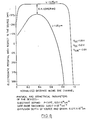
- the surface potential wlong the channel for a short channel device and a long channel device as calculated by Poisson's equation using the method of reference 3a, is shown in Figure 6. Defined in this plot is the change in the minimum value of the surface potential while the long channel device becomes a short channel device.
- the channel region of these devices was not ion-implanted.
- the doping density of the channel region was similar to that of the substrate doping. It should be noted that both devices were under subthreshold conditions. In this respect, for both the gate-to-source bias was +1.09V, with a substrate bias of -2.0V, and a drain-to-source bias of +6.0V.
- the barrier height lowering for the short channel device relative to the long channel device is clearly seen in Figure 6.
- the barrier height lowering with reference to a long channel device easily can be computed using the methods outlined in references 3a and 3b, or similar methods for any device dimension, and for each different case, by varying in many different combinations, the source and drain diffusion depths, the substrate doping, the channel-ion-implant doping density, source to drain bias and other bias conditions, and for a given channel length.
- Each combination of parameters will give different values.
- a person competent in the field of modern semiconductor MOSFET devices, with the aid of references 3a and 3b or similar methods to those outlined therein will be able to evaluate the source-barrier-height lowering.
- Photogenerated electrons 21 collected by diffusion region D1 will be injected over the barrier (LB) into the channel, as shown at 22 ( Figure 4) and finally will be drained out by drain D2 as shown at 23 ( Figure 4).
- the voltage V D1 of the region will move more positive depending on the number of electrons injected into the channel. Since the number of photogenerated electrons 21 is a function of the light intensity of the incident radiation, the voltage V D1 of the photosensing region D1 in turn is a function of the incident light intensity. Injection of electrons over the barrier LB by source D1 and the resulting voltage V D1 of source D1 is a natural logarithmic relationship.
- the photodetector structure of the present invention easily can be associated with MOSFET circuits and CCDs to form linear and area arrays.
- the signal voltage V D1 can be used easily to generate an equivalent amount of signal charge and readout by a CCD readout shift register.
- One way of utilizing a new photodetector structure to form linear and area arrays with CCD readout shift registers is shown in Figure 5.
- the photogenerated electrons normally are drained by V D2 through gate D/G.
- ST/G is at high potential and photocharge is transferred into the CCD shift register by the normal CCD transfer method.
- the arrangement shown in Figure 5 if the incoming radiation is weak, the signal can be built up by taking successive samples.
Landscapes
- Solid State Image Pick-Up Elements (AREA)
Claims (6)
Priority Applications (3)
| Application Number | Priority Date | Filing Date | Title |
|---|---|---|---|
| US06/373,972 US4473836A (en) | 1982-05-03 | 1982-05-03 | Integrable large dynamic range photodetector element for linear and area integrated circuit imaging arrays |
| DE8484303983T DE3475741D1 (en) | 1984-06-13 | 1984-06-13 | Integrable large dynamic range photodetector element for linear and area integrated circuit imaging arrays |
| EP84303983A EP0164464B1 (de) | 1982-05-03 | 1984-06-13 | Integrierbares Photodetektorelement mit hohem dynamischem Bereich für lineare und flächenhaft angeordnete integrierte Schaltkreisbildmatrizen |
Applications Claiming Priority (3)
| Application Number | Priority Date | Filing Date | Title |
|---|---|---|---|
| US06/373,972 US4473836A (en) | 1982-05-03 | 1982-05-03 | Integrable large dynamic range photodetector element for linear and area integrated circuit imaging arrays |
| JP58227096A JPS60120558A (ja) | 1983-12-02 | 1983-12-02 | 集積可能な光検出器素子 |
| EP84303983A EP0164464B1 (de) | 1982-05-03 | 1984-06-13 | Integrierbares Photodetektorelement mit hohem dynamischem Bereich für lineare und flächenhaft angeordnete integrierte Schaltkreisbildmatrizen |
Publications (2)
| Publication Number | Publication Date |
|---|---|
| EP0164464A1 EP0164464A1 (de) | 1985-12-18 |
| EP0164464B1 true EP0164464B1 (de) | 1988-12-21 |
Family
ID=27227160
Family Applications (1)
| Application Number | Title | Priority Date | Filing Date |
|---|---|---|---|
| EP84303983A Expired EP0164464B1 (de) | 1982-05-03 | 1984-06-13 | Integrierbares Photodetektorelement mit hohem dynamischem Bereich für lineare und flächenhaft angeordnete integrierte Schaltkreisbildmatrizen |
Country Status (2)
| Country | Link |
|---|---|
| US (1) | US4473836A (de) |
| EP (1) | EP0164464B1 (de) |
Families Citing this family (56)
| Publication number | Priority date | Publication date | Assignee | Title |
|---|---|---|---|---|
| US4528594A (en) * | 1983-04-20 | 1985-07-09 | Xerox Corporation | High resolution quadrilinear CCD imager |
| FR2558670B1 (fr) * | 1984-01-20 | 1986-11-21 | Thomson Csf | Perfectionnement aux dispositifs photosensibles a l'etat solide |
| WO1986003058A1 (en) * | 1984-11-13 | 1986-05-22 | Eastman Kodak Company | A solid state light sensing device |
| US4812668A (en) * | 1986-04-17 | 1989-03-14 | Honeywell Inc. | Multiplexer elements for photovoltaic detectors |
| US4973833A (en) * | 1988-09-28 | 1990-11-27 | Minolta Camera Kabushiki Kaisha | Image sensor including logarithmic converters |
| US4967249A (en) * | 1989-03-17 | 1990-10-30 | Loral Fairchild Corporation | Gain compression photodetector array |
| US4958207A (en) * | 1989-03-17 | 1990-09-18 | Loral Fairchild Corporation | Floating diode gain compression |
| US5051797A (en) * | 1989-09-05 | 1991-09-24 | Eastman Kodak Company | Charge-coupled device (CCD) imager and method of operation |
| US5241575A (en) * | 1989-12-21 | 1993-08-31 | Minolta Camera Kabushiki Kaisha | Solid-state image sensing device providing a logarithmically proportional output signal |
| US5055667A (en) * | 1990-06-21 | 1991-10-08 | Loral Fairchild Corporation | Non-linear photosite response in CCD imagers |
| KR930008528B1 (ko) * | 1990-10-13 | 1993-09-09 | 금성일렉트론 주식회사 | 고체 촬상 소자 |
| US5331164A (en) * | 1991-03-19 | 1994-07-19 | California Institute Of Technology | Particle sensor array |
| US5235197A (en) * | 1991-06-25 | 1993-08-10 | Dalsa, Inc. | High photosensitivity and high speed wide dynamic range ccd image sensor |
| EP0544260A1 (de) * | 1991-11-25 | 1993-06-02 | Eastman Kodak Company | Überlaufvorrichtung für einen CCD-Bildsensor |
| JPH05219443A (ja) * | 1992-02-05 | 1993-08-27 | Minolta Camera Co Ltd | 固体撮像装置 |
| DE4209536C3 (de) * | 1992-03-24 | 2000-10-05 | Stuttgart Mikroelektronik | Bildzelle für einen Bildaufnehmer-Chip |
| DE19519743A1 (de) * | 1994-05-31 | 1995-12-07 | Dalsa Inc | Photodetektor mit schaltungsgesteuerten CCD-Elektroden |
| US5939742A (en) * | 1997-02-10 | 1999-08-17 | Lucent Technologies Inc. | Field-effect photo-transistor |
| US6815791B1 (en) * | 1997-02-10 | 2004-11-09 | Fillfactory | Buried, fully depletable, high fill factor photodiodes |
| US20010045508A1 (en) * | 1998-09-21 | 2001-11-29 | Bart Dierickx | Pixel structure for imaging devices |
| US7199410B2 (en) * | 1999-12-14 | 2007-04-03 | Cypress Semiconductor Corporation (Belgium) Bvba | Pixel structure with improved charge transfer |
| US6011251A (en) * | 1997-06-04 | 2000-01-04 | Imec | Method for obtaining a high dynamic range read-out signal of a CMOS-based pixel structure and such CMOS-based pixel structure |
| EP0883187A1 (de) | 1997-06-04 | 1998-12-09 | Interuniversitair Micro-Elektronica Centrum Vzw | Detektor für elektromagnetische Strahlung, Pixelstruktur mit höher Empfindlichkeit mit Verwendung dieses Detektors und Verfahren zu dessen Herstellung |
| US6936849B1 (en) | 1997-07-29 | 2005-08-30 | Micron Technology, Inc. | Silicon carbide gate transistor |
| US7154153B1 (en) * | 1997-07-29 | 2006-12-26 | Micron Technology, Inc. | Memory device |
| US6794255B1 (en) | 1997-07-29 | 2004-09-21 | Micron Technology, Inc. | Carburized silicon gate insulators for integrated circuits |
| US6031263A (en) | 1997-07-29 | 2000-02-29 | Micron Technology, Inc. | DEAPROM and transistor with gallium nitride or gallium aluminum nitride gate |
| US6746893B1 (en) * | 1997-07-29 | 2004-06-08 | Micron Technology, Inc. | Transistor with variable electron affinity gate and methods of fabrication and use |
| US6965123B1 (en) | 1997-07-29 | 2005-11-15 | Micron Technology, Inc. | Transistor with variable electron affinity gate and methods of fabrication and use |
| US7196929B1 (en) | 1997-07-29 | 2007-03-27 | Micron Technology Inc | Method for operating a memory device having an amorphous silicon carbide gate insulator |
| US5929434A (en) * | 1997-08-13 | 1999-07-27 | Rockwell Science Center, Llc | Ultra-low noise high bandwidth interface circuit for single-photon readout of photodetectors |
| US7106373B1 (en) | 1998-02-09 | 2006-09-12 | Cypress Semiconductor Corporation (Belgium) Bvba | Method for increasing dynamic range of a pixel by multiple incomplete reset |
| US8063963B2 (en) * | 1998-02-09 | 2011-11-22 | On Semiconductor Image Sensor | Imaging device having a pixel structure with high dynamic range read-out signal |
| US6512544B1 (en) | 1998-06-17 | 2003-01-28 | Foveon, Inc. | Storage pixel sensor and array with compression |
| US6410899B1 (en) | 1998-06-17 | 2002-06-25 | Foveon, Inc. | Active pixel sensor with bootstrap amplification and reduced leakage during readout |
| DE19830179B4 (de) * | 1998-07-06 | 2009-01-08 | Institut für Mikroelektronik Stuttgart Stiftung des öffentlichen Rechts | MOS-Transistor für eine Bildzelle |
| US6697114B1 (en) | 1999-08-13 | 2004-02-24 | Foveon, Inc. | Triple slope pixel sensor and arry |
| US6350127B1 (en) * | 1999-11-15 | 2002-02-26 | Taiwan Semiconductor Manufacturing Company | Method of manufacturing for CMOS image sensor |
| EP1109229A3 (de) * | 1999-12-14 | 2008-03-26 | Fillfactory N.V. | Vergrabene und vollständig verarmbare Photodiode mit hohem Füllfaktor |
| GB9930257D0 (en) * | 1999-12-22 | 2000-02-09 | Suisse Electronique Microtech | Optoelectronic sensor |
| US6809768B1 (en) | 2000-02-14 | 2004-10-26 | Foveon, Inc. | Double slope pixel sensor and array |
| US6882367B1 (en) | 2000-02-29 | 2005-04-19 | Foveon, Inc. | High-sensitivity storage pixel sensor having auto-exposure detection |
| US6795117B2 (en) | 2001-11-06 | 2004-09-21 | Candela Microsystems, Inc. | CMOS image sensor with noise cancellation |
| US7233350B2 (en) * | 2002-01-05 | 2007-06-19 | Candela Microsystems, Inc. | Image sensor with interleaved image output |
| US8054357B2 (en) | 2001-11-06 | 2011-11-08 | Candela Microsystems, Inc. | Image sensor with time overlapping image output |
| US20030193594A1 (en) * | 2002-04-16 | 2003-10-16 | Tay Hiok Nam | Image sensor with processor controlled integration time |
| JP2006505159A (ja) * | 2002-10-29 | 2006-02-09 | フォトンフォーカス アクチェンゲゼルシャフト | 光電センサ |
| US7015960B2 (en) * | 2003-03-18 | 2006-03-21 | Candela Microsystems, Inc. | Image sensor that uses a temperature sensor to compensate for dark current |
| US20060166394A1 (en) * | 2003-07-07 | 2006-07-27 | Kukulka Jerry R | Solar cell structure with solar cells having reverse-bias protection using an implanted current shunt |
| US7796173B2 (en) * | 2003-08-13 | 2010-09-14 | Lettvin Jonathan D | Imaging system |
| WO2005050392A2 (en) * | 2003-11-17 | 2005-06-02 | Lettvin Jonathan D | Geometric remapping with delay lines |
| WO2006056086A1 (fr) * | 2004-11-25 | 2006-06-01 | Waeny Martin | Capteur optoelectronique a haute dynamique et faible bruit d’offset |
| US7808022B1 (en) | 2005-03-28 | 2010-10-05 | Cypress Semiconductor Corporation | Cross talk reduction |
| US7750958B1 (en) | 2005-03-28 | 2010-07-06 | Cypress Semiconductor Corporation | Pixel structure |
| US8476567B2 (en) | 2008-09-22 | 2013-07-02 | Semiconductor Components Industries, Llc | Active pixel with precharging circuit |
| US7974805B2 (en) * | 2008-10-14 | 2011-07-05 | ON Semiconductor Trading, Ltd | Image sensor and method |
Family Cites Families (19)
| Publication number | Priority date | Publication date | Assignee | Title |
|---|---|---|---|---|
| US3400383A (en) * | 1964-08-05 | 1968-09-03 | Texas Instruments Inc | Trainable decision system and adaptive memory element |
| DE1514495C3 (de) * | 1965-07-01 | 1974-10-17 | Siemens Ag, 1000 Berlin Und 8000 Muenchen | Halbleiteranordnung |
| US3453887A (en) * | 1967-02-08 | 1969-07-08 | Corning Glass Works | Temperature change measuring device |
| GB1234127A (de) * | 1968-02-19 | 1971-06-03 | ||
| US3577047A (en) * | 1969-01-15 | 1971-05-04 | Ibm | Field effect device |
| GB1323339A (en) * | 1969-09-11 | 1973-07-11 | Texas Instruments Inc | Elastic wave detector |
| JPS5035793B1 (de) * | 1970-09-11 | 1975-11-19 | ||
| US3781831A (en) * | 1972-06-30 | 1973-12-25 | Gen Electric | Read only memory utilizing floating gate transistors and method of programming |
| GB1443434A (en) * | 1973-01-22 | 1976-07-21 | Mullard Ltd | Semiconductor devices |
| US4166957A (en) * | 1974-12-17 | 1979-09-04 | Siemens Aktiengesellschaft | Apparatus and method for producing a sectional view of a body |
| US4024560A (en) * | 1975-09-04 | 1977-05-17 | Westinghouse Electric Corporation | Pyroelectric-field effect electromagnetic radiation detector |
| JPS5941351B2 (ja) * | 1976-09-13 | 1984-10-06 | 株式会社日立製作所 | カラ−用固体撮像素子 |
| DE2643968A1 (de) * | 1976-09-29 | 1978-03-30 | Siemens Ag | Matrixelement |
| JPS5370768A (en) * | 1976-12-07 | 1978-06-23 | Fujitsu Ltd | Integrated circuit |
| GB1595253A (en) * | 1977-01-24 | 1981-08-12 | Hitachi Ltd | Solid-state imaging devices |
| US4132998A (en) * | 1977-08-29 | 1979-01-02 | Rca Corp. | Insulated gate field effect transistor having a deep channel portion more highly doped than the substrate |
| US4190849A (en) * | 1977-09-19 | 1980-02-26 | Motorola, Inc. | Electronic-beam programmable semiconductor device structure |
| JPS5822901B2 (ja) * | 1978-12-01 | 1983-05-12 | 株式会社日立製作所 | 固体撮像装置 |
| JPS55128884A (en) * | 1979-03-28 | 1980-10-06 | Hitachi Ltd | Semiconductor photodetector |
-
1982
- 1982-05-03 US US06/373,972 patent/US4473836A/en not_active Expired - Lifetime
-
1984
- 1984-06-13 EP EP84303983A patent/EP0164464B1/de not_active Expired
Also Published As
| Publication number | Publication date |
|---|---|
| EP0164464A1 (de) | 1985-12-18 |
| US4473836A (en) | 1984-09-25 |
Similar Documents
| Publication | Publication Date | Title |
|---|---|---|
| US4473836A (en) | Integrable large dynamic range photodetector element for linear and area integrated circuit imaging arrays | |
| US7235831B2 (en) | Light-receiving element and photoelectric conversion device | |
| KR100371457B1 (ko) | 암전류 감소 가드링 | |
| KR100416821B1 (ko) | 고체촬상소자, 그 구동방법 및 고체촬상장치 | |
| EP0625803B1 (de) | Photodiodenstruktur | |
| CA1298389C (en) | High dynamic range charge-coupled device | |
| EP0048480B1 (de) | Halbleitender lichtelektrischer Wandler | |
| KR890004476B1 (ko) | 반도체 광검출기 장치 | |
| US5130774A (en) | Antiblooming structure for solid-state image sensor | |
| US5904493A (en) | Active pixel sensor integrated with a pinned photodiode | |
| US5898195A (en) | Solid-state imaging device of a vertical overflow drain system | |
| KR100218773B1 (ko) | 고체촬상장치 | |
| WO2000052765A1 (en) | Active pixel sensor with fully-depleted buried photoreceptor | |
| US5245203A (en) | Photoelectric converter with plural regions | |
| EP0544260A1 (de) | Überlaufvorrichtung für einen CCD-Bildsensor | |
| EP0908956B1 (de) | Photoelektrische Umwandlungsvorrichtung und Bildsensor | |
| KR20050057624A (ko) | 픽셀 이미지 센서 | |
| US4589003A (en) | Solid state image sensor comprising photoelectric converting film and reading-out transistor | |
| KR960002100B1 (ko) | 전하결합소자형 이미지센서 | |
| KR100545801B1 (ko) | 전자기 복사 탐지기, 이러한 탐지기를 사용하는 고감도 픽셀구조 및 이러한 탐지기 제조방법. | |
| US5233429A (en) | CCD image sensor having improved structure of VCCD region thereof | |
| EP0059547B1 (de) | Taktgesteuerte Vorrichtung zur Vermeidung des Überstrahlens für ladungsgekoppelte Vorrichtungen mit virtueller Phase | |
| CA1173542A (en) | Integrable large dynamic range photodetector element for linear and are a integrated circuit imaging arrays | |
| EP0118568A1 (de) | Halbleiter-bildaufzeichnungsvorrichtung | |
| WO1988002186A1 (en) | Output circuit for image sensor |
Legal Events
| Date | Code | Title | Description |
|---|---|---|---|
| PUAI | Public reference made under article 153(3) epc to a published international application that has entered the european phase |
Free format text: ORIGINAL CODE: 0009012 |
|
| AK | Designated contracting states |
Designated state(s): CH DE FR GB IT LI NL SE |
|
| 17P | Request for examination filed |
Effective date: 19851126 |
|
| RAP1 | Party data changed (applicant data changed or rights of an application transferred) |
Owner name: DALSA INC. |
|
| 17Q | First examination report despatched |
Effective date: 19870827 |
|
| GRAA | (expected) grant |
Free format text: ORIGINAL CODE: 0009210 |
|
| AK | Designated contracting states |
Kind code of ref document: B1 Designated state(s): CH DE FR GB IT LI NL SE |
|
| PG25 | Lapsed in a contracting state [announced via postgrant information from national office to epo] |
Ref country code: SE Effective date: 19881221 Ref country code: LI Effective date: 19881221 Ref country code: IT Free format text: LAPSE BECAUSE OF FAILURE TO SUBMIT A TRANSLATION OF THE DESCRIPTION OR TO PAY THE FEE WITHIN THE PRESCRIBED TIME-LIMIT;WARNING: LAPSES OF ITALIAN PATENTS WITH EFFECTIVE DATE BEFORE 2007 MAY HAVE OCCURRED AT ANY TIME BEFORE 2007. THE CORRECT EFFECTIVE DATE MAY BE DIFFERENT FROM THE ONE RECORDED. Effective date: 19881221 Ref country code: CH Effective date: 19881221 |
|
| REF | Corresponds to: |
Ref document number: 3475741 Country of ref document: DE Date of ref document: 19890126 |
|
| ET | Fr: translation filed | ||
| REG | Reference to a national code |
Ref country code: CH Ref legal event code: PL |
|
| PLBE | No opposition filed within time limit |
Free format text: ORIGINAL CODE: 0009261 |
|
| STAA | Information on the status of an ep patent application or granted ep patent |
Free format text: STATUS: NO OPPOSITION FILED WITHIN TIME LIMIT |
|
| 26N | No opposition filed | ||
| PGFP | Annual fee paid to national office [announced via postgrant information from national office to epo] |
Ref country code: GB Payment date: 19970612 Year of fee payment: 14 |
|
| PGFP | Annual fee paid to national office [announced via postgrant information from national office to epo] |
Ref country code: FR Payment date: 19970627 Year of fee payment: 14 |
|
| PGFP | Annual fee paid to national office [announced via postgrant information from national office to epo] |
Ref country code: NL Payment date: 19970630 Year of fee payment: 14 |
|
| PGFP | Annual fee paid to national office [announced via postgrant information from national office to epo] |
Ref country code: DE Payment date: 19970722 Year of fee payment: 14 |
|
| PG25 | Lapsed in a contracting state [announced via postgrant information from national office to epo] |
Ref country code: GB Free format text: LAPSE BECAUSE OF NON-PAYMENT OF DUE FEES Effective date: 19980613 |
|
| PG25 | Lapsed in a contracting state [announced via postgrant information from national office to epo] |
Ref country code: NL Free format text: LAPSE BECAUSE OF NON-PAYMENT OF DUE FEES Effective date: 19990101 |
|
| GBPC | Gb: european patent ceased through non-payment of renewal fee |
Effective date: 19980613 |
|
| PG25 | Lapsed in a contracting state [announced via postgrant information from national office to epo] |
Ref country code: FR Free format text: LAPSE BECAUSE OF NON-PAYMENT OF DUE FEES Effective date: 19990226 |
|
| NLV4 | Nl: lapsed or anulled due to non-payment of the annual fee |
Effective date: 19990101 |
|
| PG25 | Lapsed in a contracting state [announced via postgrant information from national office to epo] |
Ref country code: DE Free format text: LAPSE BECAUSE OF NON-PAYMENT OF DUE FEES Effective date: 19990401 |
|
| REG | Reference to a national code |
Ref country code: FR Ref legal event code: ST |