EP0163295A2 - A semiconductor photodetector and fabrication process for the same - Google Patents
A semiconductor photodetector and fabrication process for the same Download PDFInfo
- Publication number
- EP0163295A2 EP0163295A2 EP85106588A EP85106588A EP0163295A2 EP 0163295 A2 EP0163295 A2 EP 0163295A2 EP 85106588 A EP85106588 A EP 85106588A EP 85106588 A EP85106588 A EP 85106588A EP 0163295 A2 EP0163295 A2 EP 0163295A2
- Authority
- EP
- European Patent Office
- Prior art keywords
- layer
- semiconductor layer
- region
- mesa
- semiconductor
- Prior art date
- Legal status (The legal status is an assumption and is not a legal conclusion. Google has not performed a legal analysis and makes no representation as to the accuracy of the status listed.)
- Granted
Links
- 239000004065 semiconductor Substances 0.000 title claims description 73
- 238000000034 method Methods 0.000 title claims description 19
- 238000004519 manufacturing process Methods 0.000 title claims description 13
- 230000008569 process Effects 0.000 title claims description 6
- 229910000530 Gallium indium arsenide Inorganic materials 0.000 claims abstract description 36
- 239000012535 impurity Substances 0.000 claims description 27
- 230000005684 electric field Effects 0.000 claims description 18
- 230000015556 catabolic process Effects 0.000 abstract description 9
- 238000010521 absorption reaction Methods 0.000 abstract 1
- 239000010410 layer Substances 0.000 description 150
- 239000000758 substrate Substances 0.000 description 13
- 238000009792 diffusion process Methods 0.000 description 9
- VYPSYNLAJGMNEJ-UHFFFAOYSA-N silicon dioxide Inorganic materials O=[Si]=O VYPSYNLAJGMNEJ-UHFFFAOYSA-N 0.000 description 9
- 238000004943 liquid phase epitaxy Methods 0.000 description 7
- 239000010408 film Substances 0.000 description 6
- 230000004044 response Effects 0.000 description 6
- 230000005540 biological transmission Effects 0.000 description 5
- 229910052581 Si3N4 Inorganic materials 0.000 description 4
- 230000004888 barrier function Effects 0.000 description 4
- 229910052681 coesite Inorganic materials 0.000 description 4
- 238000004891 communication Methods 0.000 description 4
- 229910052906 cristobalite Inorganic materials 0.000 description 4
- 238000005516 engineering process Methods 0.000 description 4
- HQVNEWCFYHHQES-UHFFFAOYSA-N silicon nitride Chemical compound N12[Si]34N5[Si]62N3[Si]51N64 HQVNEWCFYHHQES-UHFFFAOYSA-N 0.000 description 4
- 229910052682 stishovite Inorganic materials 0.000 description 4
- 229910052905 tridymite Inorganic materials 0.000 description 4
- 238000000098 azimuthal photoelectron diffraction Methods 0.000 description 3
- 238000005229 chemical vapour deposition Methods 0.000 description 3
- 238000009826 distribution Methods 0.000 description 3
- 230000000694 effects Effects 0.000 description 3
- 238000002161 passivation Methods 0.000 description 3
- 238000004886 process control Methods 0.000 description 3
- 230000002441 reversible effect Effects 0.000 description 3
- 239000000377 silicon dioxide Substances 0.000 description 3
- 239000010409 thin film Substances 0.000 description 3
- RTZKZFJDLAIYFH-UHFFFAOYSA-N Diethyl ether Chemical compound CCOCC RTZKZFJDLAIYFH-UHFFFAOYSA-N 0.000 description 2
- 230000008859 change Effects 0.000 description 2
- 238000003486 chemical etching Methods 0.000 description 2
- 150000001875 compounds Chemical class 0.000 description 2
- 239000013078 crystal Substances 0.000 description 2
- 230000003247 decreasing effect Effects 0.000 description 2
- 238000006731 degradation reaction Methods 0.000 description 2
- 239000000463 material Substances 0.000 description 2
- 239000000203 mixture Substances 0.000 description 2
- 235000012239 silicon dioxide Nutrition 0.000 description 2
- 229910017401 Au—Ge Inorganic materials 0.000 description 1
- GRYLNZFGIOXLOG-UHFFFAOYSA-N Nitric acid Chemical compound O[N+]([O-])=O GRYLNZFGIOXLOG-UHFFFAOYSA-N 0.000 description 1
- 239000000969 carrier Substances 0.000 description 1
- 230000007547 defect Effects 0.000 description 1
- 230000003111 delayed effect Effects 0.000 description 1
- 238000005530 etching Methods 0.000 description 1
- 239000000835 fiber Substances 0.000 description 1
- 238000005468 ion implantation Methods 0.000 description 1
- 230000031700 light absorption Effects 0.000 description 1
- 230000000873 masking effect Effects 0.000 description 1
- 239000011259 mixed solution Substances 0.000 description 1
- 230000004048 modification Effects 0.000 description 1
- 238000012986 modification Methods 0.000 description 1
- 229910017604 nitric acid Inorganic materials 0.000 description 1
- 230000003287 optical effect Effects 0.000 description 1
- 239000010453 quartz Substances 0.000 description 1
- 230000007480 spreading Effects 0.000 description 1
- 238000003892 spreading Methods 0.000 description 1
- 238000004544 sputter deposition Methods 0.000 description 1
- 239000000126 substance Substances 0.000 description 1
- 239000002344 surface layer Substances 0.000 description 1
- 230000007704 transition Effects 0.000 description 1
Images


Classifications
-
- H—ELECTRICITY
- H01—ELECTRIC ELEMENTS
- H01L—SEMICONDUCTOR DEVICES NOT COVERED BY CLASS H10
- H01L31/00—Semiconductor devices sensitive to infrared radiation, light, electromagnetic radiation of shorter wavelength or corpuscular radiation and specially adapted either for the conversion of the energy of such radiation into electrical energy or for the control of electrical energy by such radiation; Processes or apparatus specially adapted for the manufacture or treatment thereof or of parts thereof; Details thereof
- H01L31/08—Semiconductor devices sensitive to infrared radiation, light, electromagnetic radiation of shorter wavelength or corpuscular radiation and specially adapted either for the conversion of the energy of such radiation into electrical energy or for the control of electrical energy by such radiation; Processes or apparatus specially adapted for the manufacture or treatment thereof or of parts thereof; Details thereof in which radiation controls flow of current through the device, e.g. photoresistors
- H01L31/10—Semiconductor devices sensitive to infrared radiation, light, electromagnetic radiation of shorter wavelength or corpuscular radiation and specially adapted either for the conversion of the energy of such radiation into electrical energy or for the control of electrical energy by such radiation; Processes or apparatus specially adapted for the manufacture or treatment thereof or of parts thereof; Details thereof in which radiation controls flow of current through the device, e.g. photoresistors characterised by potential barriers, e.g. phototransistors
- H01L31/101—Devices sensitive to infrared, visible or ultraviolet radiation
- H01L31/102—Devices sensitive to infrared, visible or ultraviolet radiation characterised by only one potential barrier
- H01L31/107—Devices sensitive to infrared, visible or ultraviolet radiation characterised by only one potential barrier the potential barrier working in avalanche mode, e.g. avalanche photodiodes
- H01L31/1075—Devices sensitive to infrared, visible or ultraviolet radiation characterised by only one potential barrier the potential barrier working in avalanche mode, e.g. avalanche photodiodes in which the active layers, e.g. absorption or multiplication layers, form an heterostructure, e.g. SAM structure
-
- H—ELECTRICITY
- H01—ELECTRIC ELEMENTS
- H01L—SEMICONDUCTOR DEVICES NOT COVERED BY CLASS H10
- H01L31/00—Semiconductor devices sensitive to infrared radiation, light, electromagnetic radiation of shorter wavelength or corpuscular radiation and specially adapted either for the conversion of the energy of such radiation into electrical energy or for the control of electrical energy by such radiation; Processes or apparatus specially adapted for the manufacture or treatment thereof or of parts thereof; Details thereof
- H01L31/0248—Semiconductor devices sensitive to infrared radiation, light, electromagnetic radiation of shorter wavelength or corpuscular radiation and specially adapted either for the conversion of the energy of such radiation into electrical energy or for the control of electrical energy by such radiation; Processes or apparatus specially adapted for the manufacture or treatment thereof or of parts thereof; Details thereof characterised by their semiconductor bodies
- H01L31/0352—Semiconductor devices sensitive to infrared radiation, light, electromagnetic radiation of shorter wavelength or corpuscular radiation and specially adapted either for the conversion of the energy of such radiation into electrical energy or for the control of electrical energy by such radiation; Processes or apparatus specially adapted for the manufacture or treatment thereof or of parts thereof; Details thereof characterised by their semiconductor bodies characterised by their shape or by the shapes, relative sizes or disposition of the semiconductor regions
- H01L31/035272—Semiconductor devices sensitive to infrared radiation, light, electromagnetic radiation of shorter wavelength or corpuscular radiation and specially adapted either for the conversion of the energy of such radiation into electrical energy or for the control of electrical energy by such radiation; Processes or apparatus specially adapted for the manufacture or treatment thereof or of parts thereof; Details thereof characterised by their semiconductor bodies characterised by their shape or by the shapes, relative sizes or disposition of the semiconductor regions characterised by at least one potential jump barrier or surface barrier
- H01L31/035281—Shape of the body
-
- Y—GENERAL TAGGING OF NEW TECHNOLOGICAL DEVELOPMENTS; GENERAL TAGGING OF CROSS-SECTIONAL TECHNOLOGIES SPANNING OVER SEVERAL SECTIONS OF THE IPC; TECHNICAL SUBJECTS COVERED BY FORMER USPC CROSS-REFERENCE ART COLLECTIONS [XRACs] AND DIGESTS
- Y02—TECHNOLOGIES OR APPLICATIONS FOR MITIGATION OR ADAPTATION AGAINST CLIMATE CHANGE
- Y02E—REDUCTION OF GREENHOUSE GAS [GHG] EMISSIONS, RELATED TO ENERGY GENERATION, TRANSMISSION OR DISTRIBUTION
- Y02E10/00—Energy generation through renewable energy sources
- Y02E10/50—Photovoltaic [PV] energy
Definitions
- the present invention relates to a semiconductor photodetector, more specifically, it relates to an avalanche multiplication photodiode having a buried structure.
- avalanche photodiode comprising InGaAs/InP system.
- quartz fiber light guide requires the use of light in 1 / um band, especially light of wave length of 1.3 ⁇ m or 1.6 ⁇ m.
- light of the wave length it is intended to provide a light communications system capable of transmission with a -bit-rate more than few hundreds megabits per second on a transmission span of a few tens of kilometers without a repeater.
- APD is indispensable because of its high response speed and high gain based on the avalanche multiplication of photo-induced carriers.
- the APD comprising InGaAs/InP system features the lower noise and higher response speed compared with Ge-APD, especially at 1.6 ⁇ m, thanks to the relatively larger ionization rate ratio in InP, and is expected as more suitable to the applications in the above mentioned long-span light communications.
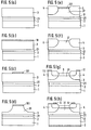
- FIG.I An exemplary configuration of InGaAs/InP APD is illustrated by the cross-section in FIG.I.
- a stacked layers of an n-type InGaAs layer 2 (the notation of the type is simply represented by n-, for example, hereinafter) and an n-InP layer 3 are formed on an InP substrate 1.
- the n-InGaAs layer 2 is for absorbing a light in 1 ⁇ m band and the n-InP layer 3 having a mesa structure 31 is for constituting an avalanche multiplication region (simply referred to as multiplication region hereinafter), as shown in FIG.l.
- There formed between the n-InGaAs layer 2 and n-InP layer 3 is an n-InGaAsP layer 21 which is for improving the response speed degradation caused by the hole pile-up at the hetero-interface, as explained later.
- n-InP layer 4 for constituting a guard ring region. That is, the mesa of n-InP layer 3 is embedded in the layer having relatively low concentration of impurity of the same conduction type.
- the n -InP layer 4 is selectively doped with a p-type impurity together with the doping of the same impurity to the mesa portion of n-InP layer 3.
- a p-type region hence, a pn junction, is formed to extend- horizontally across the layers 3 and 4.
- the reference 5 denotes the portion converted into p-type in the mesa of n-InP layer 3
- dotted line 8 denotes so-called shallow front of the diffused impurity.
- This front is a specific property of the diffusion in III-V compound semiconductor single crystals having an impurity of relatively low concentration.
- AB indicates a multiplication region including the mesa 31 of n-InP layer 3
- GR indicates a guard ring region formed in n -InP layer 4.
- an electrode 6 On the surface of the guard ring region GR is formed an electrode 6 to enclose the surface of the multiplication region AB, while on the back-side surface of the InP substrate 1 is formed another electrode 7.
- the APD can operate in an avalanche multiplication mode.
- the APD of FIG.1 has a separated structure of a light absorption layer (n-InGaAs layer 2) and an avalanche multiplication layer (n-InP layer 3), as proposed by N.Susa, et al., (see “New InGaAs/InP Avalanche Photodiodes Structure for the 1-1.6 / um Wavelength Region", IEEE Journal of Quantum Electronics, QE-16, 864, 1980).
- This structure is intended to eliminate the tunnelling current in the n-InGaAs layer.
- the tunnelling current is due to the relatively narrow band gap (0.75 eV) and small effective mass of the electrons in the n-InGaAs layer, and causes a dark current to reduce the S/N characteristic of the APD.
- the APD of FIG.1 is also formed to have a structure of the buried n-InP multiplication layer 3 as proposed by K.Yasuda, et al. including some inventors of the present invention, (see “InP/InGaAs Buried-Structure Avalanche Photodiodes", Electronic Letters, 16th February, 1984 Vol.20, No.4 pp.158-159).
- This buried structure features the high-impurity-concentration n-InP multiplication layer 3 buried in the low-impurity-concentration n -InP layer 4, thereby providing an enhanced function of the guard ring formed therein.
- the buried-structured APD is based on a principle that a pn junction formed in a semiconductor having an impurity of relatively low concentration, such as the n -InP layer 4, has a higher breakdown voltage compared with that formed in a semiconductor having an impurity of relatively higher concentration, such as n-InP layer 3.
- the depth from the surface of device to the pn junction formed in the mesa 31 of n-InP layer 3 and the n -InP layer 4 is not equal in the guard ring region GR and the multiplication region AB.
- the lower the carrier concentration or the wider the band gap in the semiconductors having the same lattice constant the deeper the pn junction formed therein by using impurity diffusion. Accordingly, the pn junction thus formed is nearer to the n-InGaAs light absorbing layer 2 in the n -InP layer 4 than in the mesa 31 of the n-InP layer 3. That is, the distance between the pn junction and the InGaAs light absorbing layer 2 is smaller in the guard ring region GR compared with in the multiplication region AB, and the effective thickness of the n -InP layer 4 is decreased.
- the InP substrate 1 is provided with an impurity of high concentration (e.g. order of 10 18 cm -3 compared with 10 15 to 10 16 cm -3 in the n-InGaAs light absorbing layer 2, n-InP layer 3, etc.), therefore, when an external reverse bias voltage is applied between the electrodes 6 and 7, the depletion layer spreads from the pn junction toward the interface of the n-InGaAs layer 2 and n-InP substrate 1.
- the electrical field generated in the guard ring region GR is stronger than that formed in the multiplication region AB because of the unevenness of the pn junction in the multiplication region AB and guard ring region GR.
- the electrical field distribution in the APD must be designed so that the field in the n-InP layer 3, especially in the depletion layer near the pn junction in the mesa 31, must be large enough to cause avalanche multiplication, and the respective electrical fields in the n-InGaAsP layer 21 and n-InGaAs layer 2, in particular, at the respective hetero-interfaces, must be small enough to suppress the tunnelling current in the layers.
- the pn junction in the guard ring region is required not to cause breakdown by the application of the external reverse bias voltage to cause the avalanche multiplication.
- the electrical fields at the respective hetero-interfaces must properly be adjusted to correlate one another in view of dark current due to the tunnelling electrons and the aforesaia hole pile-up phenomena. If n-InGaAs layer 2 directly interfaces n-InP layer 3, a valence band discontinuity forming a barrier of height of about 0.4 eV appears. This barrier acts as a trap for the holes generated in the n-InGaAs light absorbing layer 2, and the delayed release of holes from the trap affects to decrease the response speed of the APD.
- a certain magnitude of electrical field is required at the hetero-interface between the n-InGaAs layer 2 and n-InP layer 3 in order to provide the holes with sufficient energy to surmount the barrier.
- the estimated value for this electrical field is about 3 x 10 5 V/cm or more for an interface made on the (111)A-oriented surface of an InP substrate by using a liquid phase epitaxy (LPE) technique, for example.
- LPE liquid phase epitaxy
- the electrical field necessary to suppress the tunnelling electrons through the n-InGaAs layer 2 must be less than about 2.3 x 10 5 V/cm.
- the antinomy in the requirements for the electrical fields is dissolved by introducing an intermediate n-InGaAsP layer 21 which reduces the effective barrier height between the hetero-interface of the n-InGaAs layer 2 and InP layer 3, thereby improving the response speed degradation caused by the hole pile-up at the hetero-interface.
- transition layer in which the energy band gap is continuously changed from 1.35 eV of InP to 0.75 eV of InGaAs, can be used to substitute for the n-InGaAsP intermediate layer 21.
- the electrical field at the hetero-interface of the n-InGaAsP layer 21 and the n-InP layer 3 must be between 3.5 x 10 5 and 2.5 x 10 5 V/cm, and that at the hetero-interface of the n-InGaAsP layer 21 and n-InGaAs layer 2 must be between 2.3 x 10⁵ and 1.5 x 10 5 V/cm, when each of the layers are formed on an (111)-oriented surface of the InP substrate 1 by using a conventional LPE technique under the conditions for dissolution- free, for example.
- the parameters include, for example, the respective thicknesses of and the impurity concentrations in each of the layers 2, 21, 3 and 4 and the diffusion depth of the impurity for creating the pn junction.
- the operational margin of the APD is inevitably reduced.
- the above objects can be attained by providing a buried-structure APD with a surface level difference between the multiplication region and guard ring region wherein the surface of the multiplication region is lowered than that of the guard ring region. More precisely, a first semiconductor layer having an impurity of relatively high concentration is formed on a light absorbing layer and is then formed into a mesa structure for constituting a multiplication region, and a second semiconductor layer having the same conductivity type impurity of relatively low concentration is formed around the mesa of the first semiconductor layer so that the mesa is embedded therein.
- the surface level difference is provided by selectively growing the second semiconductor layer by forming a mask on the surface of the mesa in advance, or selectively removing the surface of the second semiconductor layer on the mesa instead.
- the pn junction formed to extend across the multiplication region and guard ring region is in an equal level or is made far from the light absorbing layer in the guard ring region compared with in the multiplication region, thereby eliminating the aforesaid problem due to difficulties in the control of the electrical fields at each hetero-interface in the conventional APD.
- FIG.2 is a cross-section of an APD according to the present invention.
- the configuration of the APD in FIG.2 is almost the same as shown in FIG.1, and like references designate like or corresponding parts in FIG.1.
- the APD of FIG.2 there is provided a level difference between the respective surfaces of the multiplication region AB and the guard ring region GR so that the surface level of the multiplication region AB is lower than that in the guard ring region GR. Moreover, a slope 9 is provided between the surfaces. Hence, the pn junction in the mesa 31 of the n-InP layer 3 (the first semiconductor layer) and that in the n - -InP layer 4 (the second semiconductor layer) are formed substantially in the same level, thanks to the aforementioned surface level difference.
- the pn junction formed by an impurity diffusion is deeper in a layer such as the n -InP layer 4 having relatively low carrier concentration than in a layer such as the n-InP layer 3 having relatively high carrier concentration, accordingly, deeper pn junction is formed in the n -InP layer 4 compared with in the mesa 31 of the n-InP layer 3.
- the value of the surface level difference between the multiplication region AB and guard ring region GR is determined according to the relation between the depth of pn junction formed by the diffusion of a p-type impurity as the function of carrier concentration in InP layer.
- the respective electrical field distributions in the multiplication region AB and the guard ring region GR are made closely similar, and therefore, the the electrical field at each hetero-interface between the n-InP layer 3 and n-InGaAsP layer 21, or between the n-InGaAsP layer 21 and n-InGaAs layer 2 is almost or substantially equal throughout the multiplication region AB and the guard ring region GR.
- the breakdown voltage difference of the pn junction in the multiplication region AB and guard ring region GR is still maintained or can be increased than the APD as shown in F I G . 1 .
- the higher breakdown voltage of the pn junction in the guard ring region can also be obtained with the use of a semiconductor having relatively wider energy band gap ( ⁇ g ) for constituting the guard ring region.
- FIG.3 is a cross-section showing a second embodiment of an APD according to the present invention.
- This embodiment is intended to enhance the effect of the surface level difference between the multiplication region AB and guard ring region GR as provided in the first embodiment.
- the pn junction is not formed in an equal level throughout the multiplication region AB and the guard ring region GR but is formed so that its distance to the light absorbing layer is larger in the guard ring region than in the multiplication region.
- the surface level difference is determined so that the pn junction is formed in the same level throughout the multiplication region and guard ring region, however, in the APD shown in FIG.3, further larger level difference is provided between the respective surfaces of the multiplication region AB and the guard ring region GR. Accordingly, when a p-type impurity is diffused from the surfaces of the multiplication region AB and guard ring region GR, the distance of the pn junction formed therewith to the n-InGaAs light absorbing layer 2 is relatively larger in the n -- InP layer 4 than in the mesa 31 of n-InP layer 3.
- the electrical field strength at each hetero-interface in the guard ring region GR can certainly be weaker compared with each corresponding hetero-interface in the multiplication region AB.
- the breakdown voltage difference between -the multiplication region AB and guard ring region GR is increased compared with that in the first embodiment.
- the slope 9 between the respective surfaces of the multiplication region AB and guard ring region GR provides a gradual level change of pn junction between the multiplication region AB and guard ring region GR.
- the larger radius of curvature of the pn junction is advantageous for preventing the local-breakdown which is probable in the pn junction having abrupt level change as in FIG.1, thereby improving the reliability of the APDs according to the present invention.
- FIG.4 is a cross-section showing a third embodiment of an APD according to the present invention.
- the second semiconductor layer 4 for example,, an n -InP layer
- the first semiconductor layer 3 for example, n-InP layer
- the surface level difference between the multiplication region AB and the guard ring region GR is provided similar to the previous embodiments.
- FIG.4 Although shown in FIG.4 is an APD having unleveled pn junction extending across the mesa - 31 of the n-InP layer 3 to the n -InP layer 4, depending on the magnitude of the surface level difference provided between the multiplication region AB and guard ring region GR, the object of this embodiment is not affected if the pn junction is formed in the same level throughout the multiplication region AB and guard ring region GR as in the APD of the first embodiment shown in FIG.2.
- the configuration of the third embodiment shown in FIG.4 is advantageous for the fabrication of the APD, because the magnitude of the surface level difference can be properly adjusted in cut and try method during selectively removing the surface layer of the multiplication region AB. This means that the conditions for growing the n -InP layer 4 can be independent from the parameters for providing the necessary surface level difference.
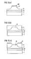
- FIGs.5(a) to 5(h) show* the fabrication steps of the APD of the first embodiment, each illustrating the cross-section at one step. Details of the steps are described in the following with reference to the figures.
- the n-InGaAs layer 2 and n-InGaAsP layer 21 have carrier concentration of 1 x 10 16 cm -3 .
- the thickness of the n-InGaAs layer 2 and n-InGaAsP layer 21 are 1.5 ⁇ m and 0.5 ⁇ m, respectively.
- the n-InP layer 3 has a carrier concentration of 1.5 x 10 16 cm -3 and thickness of 3 ⁇ m.
- These layers 2, 21 and 3 are grown to match the lattice of the (lll)A-oriented surface of the InP substrate 1.
- Exemplary compositions of the n-InGaAs layer 2 and n-InGaAsP layer 21 are In 0.47 Ga 0.53 As and In 0.67 Ga 0.33 As 0.70 P 0.30 , respectively.
- another mask layer 12 (a Si0 2 film, for example,) is selectively formed on the surface of the second semiconductor layer 4 except the region on the top of the mesa 31, as shown in FIG.6(c), by using a conventional thin film technology and photolithographic method.
- the unmasked surface of the second semiconductor layer 4 is, then, removed by a conventional chemical or other etching technique, until a predetermined magnitude of surface level difference, for example, 0.3 ⁇ m, or more, is provided between the respective surfaces of the unmasked and the masked portions.
- the maximum thickness of the second semiconductor layer 4 grown during the step of FIG.6(b) is large enough to provide a sufficient level difference, more than 0.3 , p m, between the respective surfaces on the mesa 31 and the region around the mesa 31, the pn junction formed to extend across the mesa 31 to the second semiconductor layer 4 can be unleveled as in the case shown in FIG.5(h).
- the APD of the present invention since the APD of the present invention has a pn junction formed to extend across a multiplication region to a guard ring region substantially in the same level or formed farther apart from a light absorbing layer in the guard ring region than in the multiplication region, the electrical field at each hetero-interface in the guard ring region can substantially be equal to or weaker than that at each corresponding hetero-interface in the multiplication region. Moreover, the breakdown voltage difference of the pn junction in the multiplication region and guard ring region is increased because of the increased distance between the pn junction and the hetero-interface in the guard ring region. Accordingly, the allowances in the design and process control in the fabrication and the operational margin of the APD can be increased.
- the dark current mainly caused by the tunnel current at the hetero-interfaces in the guard ring region, has been reduced to be in the range of 10 to 30 nA compared with 50 to 100 nA of the conventional APD, in average, without loosing the guard ring effect achieved by the buried structure.
- intermediate layer 21 is provided in the all embodiments, it can be omitted so that the multiplication layer 3 is formed directly on the absorbing layer 2, when the absorbing layer 2 is composed of an InGaAsP.
- each of the semiconductor layers constituting an APD according to the present invention is not limited to the materials described in the above but could be selected from another III-V group compound semiconductor materials.
Landscapes
- Physics & Mathematics (AREA)
- Condensed Matter Physics & Semiconductors (AREA)
- Electromagnetism (AREA)
- General Physics & Mathematics (AREA)
- Engineering & Computer Science (AREA)
- Computer Hardware Design (AREA)
- Microelectronics & Electronic Packaging (AREA)
- Power Engineering (AREA)
- Light Receiving Elements (AREA)
Abstract
Description
- The present invention relates to a semiconductor photodetector, more specifically, it relates to an avalanche multiplication photodiode having a buried structure.
- In the photodetectors for long-distance light communications systems, most promising one is the avalanche photodiode (APD) comprising InGaAs/InP system.
- The maximum utilization of the optical transmission characteristics of quartz fiber light guide requires the use of light in 1 /um band, especially light of wave length of 1.3 µm or 1.6 µm. By using light of the wave length, it is intended to provide a light communications system capable of transmission with a -bit-rate more than few hundreds megabits per second on a transmission span of a few tens of kilometers without a repeater. For such long transmission span, APD is indispensable because of its high response speed and high gain based on the avalanche multiplication of photo-induced carriers.
- In a short span light communication systems for 1 µm band, Ge-APD is already put into practical use, however, its relatively low S/N ratio characteristic limits the use in the transmission of long span. On the ether hand, the APD comprising InGaAs/InP system features the lower noise and higher response speed compared with Ge-APD, especially at 1.6 µm, thanks to the relatively larger ionization rate ratio in InP, and is expected as more suitable to the applications in the above mentioned long-span light communications.
- An exemplary configuration of InGaAs/InP APD is illustrated by the cross-section in FIG.I. Referring to FIG.1, a stacked layers of an n-type InGaAs layer 2 (the notation of the type is simply represented by n-, for example, hereinafter) and an n-
InP layer 3 are formed on anInP substrate 1. The n-InGaAs layer 2 is for absorbing a light in 1 µm band and the n-InP layer 3 having amesa structure 31 is for constituting an avalanche multiplication region (simply referred to as multiplication region hereinafter), as shown in FIG.l. There formed between the n-InGaAs layer 2 and n-InP layer 3 is an n-InGaAsP layer 21 which is for improving the response speed degradation caused by the hole pile-up at the hetero-interface, as explained later. - Around the
mesa 31 of the n-InP layer 3 is formed an n -InP layer 4 for constituting a guard ring region. That is, the mesa of n-InP layer 3 is embedded in the layer having relatively low concentration of impurity of the same conduction type. The n -InP layer 4 is selectively doped with a p-type impurity together with the doping of the same impurity to the mesa portion of n-InP layer 3. Thus, a p-type region, hence, a pn junction, is formed to extend- horizontally across thelayers - In FIG.1, the
reference 5 denotes the portion converted into p-type in the mesa of n-InP layer 3, and dottedline 8 denotes so-called shallow front of the diffused impurity. This front is a specific property of the diffusion in III-V compound semiconductor single crystals having an impurity of relatively low concentration. Also, AB indicates a multiplication region including themesa 31 of n-InP layer 3 and GR indicates a guard ring region formed in n -InP layer 4. - On the surface of the guard ring region GR is formed an
electrode 6 to enclose the surface of the multiplication region AB, while on the back-side surface of theInP substrate 1 is formed anotherelectrode 7. When a sufficient magnitude of a reverse bias voltage along the direction from theInP substrate 1 to the p-type region 5 is applied between theelectrodes - The APD of FIG.1 has a separated structure of a light absorption layer (n-InGaAs layer 2) and an avalanche multiplication layer (n-InP layer 3), as proposed by N.Susa, et al., (see "New InGaAs/InP Avalanche Photodiodes Structure for the 1-1.6 /um Wavelength Region", IEEE Journal of Quantum Electronics, QE-16, 864, 1980). This structure is intended to eliminate the tunnelling current in the n-InGaAs layer. The tunnelling current is due to the relatively narrow band gap (0.75 eV) and small effective mass of the electrons in the n-InGaAs layer, and causes a dark current to reduce the S/N characteristic of the APD.
- The APD of FIG.1 is also formed to have a structure of the buried n-
InP multiplication layer 3 as proposed by K.Yasuda, et al. including some inventors of the present invention, (see "InP/InGaAs Buried-Structure Avalanche Photodiodes", Electronic Letters, 16th February, 1984 Vol.20, No.4 pp.158-159). This buried structure features the high-impurity-concentration n-InP multiplication layer 3 buried in the low-impurity-concentration n -InP layer 4, thereby providing an enhanced function of the guard ring formed therein. The buried-structured APD is based on a principle that a pn junction formed in a semiconductor having an impurity of relatively low concentration, such as the n -InP layer 4, has a higher breakdown voltage compared with that formed in a semiconductor having an impurity of relatively higher concentration, such as n-InP layer 3. - However, in the APD of FIG.1, the depth from the surface of device to the pn junction formed in the
mesa 31 of n-InP layer 3 and the n -InP layer 4 is not equal in the guard ring region GR and the multiplication region AB. There is a general characteristics that the lower the carrier concentration or the wider the band gap in the semiconductors having the same lattice constant, the deeper the pn junction formed therein by using impurity diffusion. Accordingly, the pn junction thus formed is nearer to the n-InGaAslight absorbing layer 2 in the n -InP layer 4 than in themesa 31 of the n-InP layer 3. That is, the distance between the pn junction and the InGaAslight absorbing layer 2 is smaller in the guard ring region GR compared with in the multiplication region AB, and the effective thickness of the n -InP layer 4 is decreased. - In the APD as shown in FIG.l, the
InP substrate 1 is provided with an impurity of high concentration (e.g. order of 1018 cm-3 compared with 1015 to 1016 cm-3 in the n-InGaAslight absorbing layer 2, n-InP layer 3, etc.), therefore, when an external reverse bias voltage is applied between theelectrodes InGaAs layer 2 and n-InP substrate 1. This means that the electrical field generated in the guard ring region GR is stronger than that formed in the multiplication region AB because of the unevenness of the pn junction in the multiplication region AB and guard ring region GR. - This unevenness of the pn junction in the multiplication region AB and guard ring region GR is probable even when an ion implantation or epitaxial growth technology is employed for forming pn junction because of the accompanying thermal process to anneal and activate the impurities.
- It is important for the design of APD that the electrical field distribution in the APD must be designed so that the field in the n-
InP layer 3, especially in the depletion layer near the pn junction in themesa 31, must be large enough to cause avalanche multiplication, and the respective electrical fields in the n-InGaAsP layer 21 and n-InGaAs layer 2, in particular, at the respective hetero-interfaces, must be small enough to suppress the tunnelling current in the layers. Moreover, the pn junction in the guard ring region is required not to cause breakdown by the application of the external reverse bias voltage to cause the avalanche multiplication. - Furthermore, the electrical fields at the respective hetero-interfaces must properly be adjusted to correlate one another in view of dark current due to the tunnelling electrons and the aforesaia hole pile-up phenomena. If n-
InGaAs layer 2 directly interfaces n-InP layer 3, a valence band discontinuity forming a barrier of height of about 0.4 eV appears. This barrier acts as a trap for the holes generated in the n-InGaAslight absorbing layer 2, and the delayed release of holes from the trap affects to decrease the response speed of the APD. In other words, a certain magnitude of electrical field is required at the hetero-interface between the n-InGaAs layer 2 and n-InP layer 3 in order to provide the holes with sufficient energy to surmount the barrier. The estimated value for this electrical field is about 3 x 10⁵ V/cm or more for an interface made on the (111)A-oriented surface of an InP substrate by using a liquid phase epitaxy (LPE) technique, for example. - However, the electrical field necessary to suppress the tunnelling electrons through the n-
InGaAs layer 2 must be less than about 2.3 x 10⁵ V/cm. The antinomy in the requirements for the electrical fields is dissolved by introducing an intermediate n-InGaAsP layer 21 which reduces the effective barrier height between the hetero-interface of the n-InGaAs layer 2 andInP layer 3, thereby improving the response speed degradation caused by the hole pile-up at the hetero-interface. (See "InGaAs Avalanche Photodiodes for 1 /um Wavelength Region" Electronics Letters, 7th July 1983, Vol.19, No.14, pp.534-536, by T. Shirai, et al. including some inventors of the present invention.) As an equivalent, so-called transition layer, in which the energy band gap is continuously changed from 1.35 eV of InP to 0.75 eV of InGaAs, can be used to substitute for the n-InGaAsPintermediate layer 21. - In the APD of FIG.1, to suppress the tunnelling current and the hole pile-up, the electrical field at the hetero-interface of the n-
InGaAsP layer 21 and the n-InP layer 3 must be between 3.5 x 10⁵ and 2.5 x 10 5 V/cm, and that at the hetero-interface of the n-InGaAsP layer 21 and n-InGaAs layer 2 must be between 2.3 x 10⁵ and 1.5 x 10⁵ V/cm, when each of the layers are formed on an (111)-oriented surface of theInP substrate 1 by using a conventional LPE technique under the conditions for dissolution- free, for example. - These electrical field conditions must be satisfied in each of the multiplication region AB and guard ring region GR. However, the difference in the electrical field distributions in the multiplication region and guard ring region due to the unevenness of pn junction and the difference in the carrier concentrations of the multiplication region AB and guard ring region GR imposes difficulties on the design, fabrication and operation of the APD.
- That is, the allowances of the design parameters of the APD are decreased and severe process controls to achieve these design parameters. The parameters include, for example, the respective thicknesses of and the impurity concentrations in each of the
layers - It is an object of the present invention to provide an APD for 1 1um band with the characteristics of high S/N ratio and high response speed.
- It is another object of the present invention to provide a buried-structure APD having a pn junction extending across the multiplication region and the guard ring region substantially in parallel to the interface of buried multiplication layer and light absorbing layer, wherein the distance between the pn junction and the interface in the multiplication region is substantially equal to or smaller than that in the guard ring region.
- It is still another object of the present invention to provide a buried-structure APD having large operational margin.
- It is yet another object of the present invention to provide a method for fabricating a buried-structure APD of high yield and low cost.
- It is still yet another object of the present invention to provide a method for fabricating a buried-structure APD of high reliability.
- The above objects can be attained by providing a buried-structure APD with a surface level difference between the multiplication region and guard ring region wherein the surface of the multiplication region is lowered than that of the guard ring region. More precisely, a first semiconductor layer having an impurity of relatively high concentration is formed on a light absorbing layer and is then formed into a mesa structure for constituting a multiplication region, and a second semiconductor layer having the same conductivity type impurity of relatively low concentration is formed around the mesa of the first semiconductor layer so that the mesa is embedded therein. The surface level difference is provided by selectively growing the second semiconductor layer by forming a mask on the surface of the mesa in advance, or selectively removing the surface of the second semiconductor layer on the mesa instead. In the APD of the present invention, the pn junction formed to extend across the multiplication region and guard ring region is in an equal level or is made far from the light absorbing layer in the guard ring region compared with in the multiplication region, thereby eliminating the aforesaid problem due to difficulties in the control of the electrical fields at each hetero-interface in the conventional APD.
- The above and other objects and advantages cf the present invention will be more apparent from the following description of preferred embodiments with reference to the accompanying drawings, wherein:
- FIG.l is a cross-section showing an exemplary configuration of an InGaAs/InP APD;
- FIG.2 is a cross-section of an APD according to the present invention.
- FIG.3 is a cross-section showing a second embodiment of the APD according to the present invention.
- FIG.4 is a cross-section showing a third embodiment of an APD according to the present invention.
- FIGs.5(a) to 5(h) show the fabrication steps of the - APD of the first embodiment, illustrating a cross-section at each step.
- FIGs. 6 (a) to 6 (c) show the fabrication steps of the APD of the third embodiment, illustrating a cross-section at each step.
- FIG.2 is a cross-section of an APD according to the present invention. The configuration of the APD in FIG.2 is almost the same as shown in FIG.1, and like references designate like or corresponding parts in FIG.1.
- However, in the APD of FIG.2, there is provided a level difference between the respective surfaces of the multiplication region AB and the guard ring region GR so that the surface level of the multiplication region AB is lower than that in the guard ring region GR. Moreover, a
slope 9 is provided between the surfaces. Hence, the pn junction in themesa 31 of the n-InP layer 3 (the first semiconductor layer) and that in the n- -InP layer 4 (the second semiconductor layer) are formed substantially in the same level, thanks to the aforementioned surface level difference. That is, as described before, the pn junction formed by an impurity diffusion is deeper in a layer such as the n -InP layer 4 having relatively low carrier concentration than in a layer such as the n-InP layer 3 having relatively high carrier concentration, accordingly, deeper pn junction is formed in the n -InP layer 4 compared with in themesa 31 of the n-InP layer 3. In other word, the value of the surface level difference between the multiplication region AB and guard ring region GR is determined according to the relation between the depth of pn junction formed by the diffusion of a p-type impurity as the function of carrier concentration in InP layer. - If the pn junction is made extend in the same level across the
mesa 31 to the n -InP layer 4, the respective electrical field distributions in the multiplication region AB and the guard ring region GR are made closely similar, and therefore, the the electrical field at each hetero-interface between the n-InP layer 3 and n-InGaAsP layer 21, or between the n-InGaAsP layer 21 and n-InGaAs layer 2 is almost or substantially equal throughout the multiplication region AB and the guard ring region GR. In this configuration, the breakdown voltage difference of the pn junction in the multiplication region AB and guard ring region GR is still maintained or can be increased than the APD as shown in FIG.1. - The higher breakdown voltage of the pn junction in the guard ring region can also be obtained with the use of a semiconductor having relatively wider energy band gap (εg) for constituting the guard ring region. For example, a layer of an n-Al0.48Ga0.52As (εg = 1.45 eV) can be used to substitute for the n -InP layer 4 (εg = 1.35 eV).
- FIG.3 is a cross-section showing a second embodiment of an APD according to the present invention. This embodiment is intended to enhance the effect of the surface level difference between the multiplication region AB and guard ring region GR as provided in the first embodiment. In this second embodiment, compared with the first embodiment, the pn junction is not formed in an equal level throughout the multiplication region AB and the guard ring region GR but is formed so that its distance to the light absorbing layer is larger in the guard ring region than in the multiplication region.
- In the APD of FIG.2, the surface level difference is determined so that the pn junction is formed in the same level throughout the multiplication region and guard ring region, however, in the APD shown in FIG.3, further larger level difference is provided between the respective surfaces of the multiplication region AB and the guard ring region GR. Accordingly, when a p-type impurity is diffused from the surfaces of the multiplication region AB and guard ring region GR, the distance of the pn junction formed therewith to the n-InGaAs
light absorbing layer 2 is relatively larger in the n--InP layer 4 than in themesa 31 of n-InP layer 3. As a result, the electrical field strength at each hetero-interface in the guard ring region GR can certainly be weaker compared with each corresponding hetero-interface in the multiplication region AB. This means that the restriction on the electrical field to suppress tunnelling current can substantially be eliminated. And the breakdown voltage difference between -the multiplication region AB and guard ring region GR is increased compared with that in the first embodiment. Hence, the allowances in the design and process control and the operational margin can be extended further in this - The
slope 9 between the respective surfaces of the multiplication region AB and guard ring region GR provides a gradual level change of pn junction between the multiplication region AB and guard ring region GR. The larger radius of curvature of the pn junction is advantageous for preventing the local-breakdown which is probable in the pn junction having abrupt level change as in FIG.1, thereby improving the reliability of the APDs according to the present invention. - FIG.4 is a cross-section showing a third embodiment of an APD according to the present invention. In this embodiment, the
second semiconductor layer 4, for example,, an n -InP layer, is formed on and around the mesa of thefirst semiconductor layer 3, for example, n-InP layer, wherein the surface level difference between the multiplication region AB and the guard ring region GR is provided similar to the previous embodiments. Although shown in FIG.4 is an APD having unleveled pn junction extending across the mesa - 31 of the n-InP layer 3 to the n -InP layer 4, depending on the magnitude of the surface level difference provided between the multiplication region AB and guard ring region GR, the object of this embodiment is not affected if the pn junction is formed in the same level throughout the multiplication region AB and guard ring region GR as in the APD of the first embodiment shown in FIG.2. - The configuration of the third embodiment shown in FIG.4 is advantageous for the fabrication of the APD, because the magnitude of the surface level difference can be properly adjusted in cut and try method during selectively removing the surface layer of the multiplication region AB. This means that the conditions for growing the n -
InP layer 4 can be independent from the parameters for providing the necessary surface level difference. - FIGs.5(a) to 5(h) show* the fabrication steps of the APD of the first embodiment, each illustrating the cross-section at one step. Details of the steps are described in the following with reference to the figures.
- (a) By employing a liquid-phase epitaxy (LPE) technique, for example, each of an n-InGaAs
light absorbing layer 2, n-InGaAsPintermediate layer 21 and n-InPavalanche multiplication layer 3 is grown to form a stacked structure on anInP substrate 1 as shown in FIG.5(a). TheInP substrate 1 has a carrier concentration of 2 x 10¹⁸ (cm-3)and surface orientation of (111)A. Between theInP substrate 1 and the n-InGaAs layer 2 is formed an n-InP buffer layer (not shown) to ease the influence due to the defects existing on the surface of theInP substrate 1. - The n-
InGaAs layer 2 and n-InGaAsP layer 21 have carrier concentration of 1 x 1016 cm-3. The thickness of the n-InGaAs layer 2 and n-InGaAsP layer 21 are 1.5 µm and 0.5 µm, respectively. The n-InP layer 3 has a carrier concentration of 1.5 x 1016 cm-3 and thickness of 3µm. Theselayers InP substrate 1. Exemplary compositions of the n-InGaAs layer 2 and n-InGaAsP layer 21 are In0.47Ga0.53 As and In0.67 Ga0.33 As0.70 P0.30, respectively. - (b) A protecting film 10 of silicon dioxide (Si02) or silicon nitride (Si3N4) of a thickness in the range of 600 A to 2000 A is formed on the surface of the n-
InP layer 3, as shown in FIG.5(b), by using a conventional thin film technology including sputtering, chemical vapor deposition (CVD) or plasma excited CVD method. - (c) The protecting film 10 is selectively removed by a conventional photolithographic technique, thereby a pattern (mask) 101 of the film, for example, a circle having diameter of 100 µm, is formed, as shown in FIG.5(c).
- (d) By contacting an In-P molten mixture having degree of unsaturation of 10°C, the unmasked portion of the n-
InP layer 3 is selectively removed (melt-back). Thus, amesa structure 31 of theInP layer 3 is formed under the masked portion as shown in FIG.5(d). The maximum depth of the portion removed by the melt-back is about 2.5 µm. According to the melt-back method, the side surface of themesa 31 usually has a slope spreading downward due to the sideward melt-back effect. - (e) An n -
InP layer 4 is selectively grown on the surface of the removed portion of the n-InP layer 3, as shown in FIG.5(e), by using a conventional LPE technique, for example. This selective growth is easy thanks to themask 101 on which any crystal growth does not take place. As a result, the n -InP layer 4 having a flat surface in parallel to the n-InGaAs layer 2 is obtained. The maximum thickness of the n -InP layer 4 on the melt-backed surface of the n-InP layer 3 is approximately 2.8 µm, therefore, the surface level of the unmasked portion is about 0.3 µm higher than that of the maked portion. - (f) The
mask 101 on themesa 31 is removed as shown in FIG.5(f) by an appropriate chemical etching, for example. If thefilm 101 is composed of SiO2 or Si3N4, a mixed solution of HNO3 and HF of 1 : 1 in weight ratio can be used. - (g) Another masking layer (for example, SiO2 film) 11 is selectively formed on the surface of the n -
InP layer 4 except a predetermined area of the surface of n -InP layer 4 around themesa 31 is exposed, and then, a p-type impurity is thermally diffused from the unmasked surface by using a conventional diffusion technique. Hence, respective p-type regions are formed in themesa 31 and the n -InP layer 4, as shown in FIG.5(g). In the impurity diffusion, gaseous CdP2, for example, as the source of the p-type impurity, is introduced into a closed tube heated at a temperature of 500 to 550°C. The diffusion depth of the p-type impurity is controlled to be 1.5 µm in themesa 31 and 1.8 µm in the n -InP layer 4. Thus, the pn junction formed as above extends substantially in the same level across themesa 31 of the n-InP layer 3 to the n -InP layer 4. The p-type-impurity-dopedregion 5 of themesa 31 functions as the window for the light sensitive region of the APD. - (h) A passivation layer (not shown) of Si3N4, for example, is coated on the entire surfaces of the
mesa 31 and n -InP layer 4 by using a conventional thin film technology. Then, anohmic electrode 6 of Au-Zn, for example, is formed on the surface of the n- -InP layer 4 around the surface of themesa 31 through the window formed in the passivation layer. Anotherohmic electrode 7 of Au-Ge, for example, is formed on the back-side surface of theInP substrate 1, as shown in FIG.5(h). Thus, the APD of the first embodiment is completed. - FIG.6(a) to 6(c) show the fabrication steps of the APD of the third embodiment, illustrating the cross-section at each step. Details of the steps are described in the following with reference to the figures.
- FIG.6 (a) show a structure of the APD at the step equivalent to FIG.5(d). Different from the previous embodiments, the
mask 101 is removed by using an appropriate chemical etching as described with reference to the step of FIG.5(f), and then, asecond semiconductor layer 4, for example, an n -InP layer, is grown by using a LPE method so that themesa 31 of thefirst semiconductor layer 3 is completely buried therein, as shown in FIG.6(b). The maximum thickness of thesecond semiconductor layer 4 is about 2.8 µm, for the height of themesa 31 is 2.5 µm. Thesecond semiconductor layer 4 thus formed on themesa 31 usually has a substantially flat surface. - Following the above, another mask layer 12 (a Si02 film, for example,) is selectively formed on the surface of the
second semiconductor layer 4 except the region on the top of themesa 31, as shown in FIG.6(c), by using a conventional thin film technology and photolithographic method. The unmasked surface of thesecond semiconductor layer 4 is, then, removed by a conventional chemical or other etching technique, until a predetermined magnitude of surface level difference, for example, 0.3 µm, or more, is provided between the respective surfaces of the unmasked and the masked portions. - By removing the
mask layer 12, the structure equivalent to FIG.5(f) is obtained. Subsequent steps including those for p-type impurity diffusion as shown in FIG.5(g), aforementioned surface passivation and the electrode forming as shown in FIG.5(h) follow the above step, and the third embodiment APD is completed. - If the maximum thickness of the
second semiconductor layer 4 grown during the step of FIG.6(b) is large enough to provide a sufficient level difference, more than 0.3 ,pm, between the respective surfaces on themesa 31 and the region around themesa 31, the pn junction formed to extend across themesa 31 to thesecond semiconductor layer 4 can be unleveled as in the case shown in FIG.5(h). - As disclosed in the above embodiments, since the APD of the present invention has a pn junction formed to extend across a multiplication region to a guard ring region substantially in the same level or formed farther apart from a light absorbing layer in the guard ring region than in the multiplication region, the electrical field at each hetero-interface in the guard ring region can substantially be equal to or weaker than that at each corresponding hetero-interface in the multiplication region. Moreover, the breakdown voltage difference of the pn junction in the multiplication region and guard ring region is increased because of the increased distance between the pn junction and the hetero-interface in the guard ring region. Accordingly, the allowances in the design and process control in the fabrication and the operational margin of the APD can be increased. As a result, in the APD according to the present invention, the dark current, mainly caused by the tunnel current at the hetero-interfaces in the guard ring region, has been reduced to be in the range of 10 to 30 nA compared with 50 to 100 nA of the conventional APD, in average, without loosing the guard ring effect achieved by the buried structure.
- Although
intermediate layer 21 is provided in the all embodiments, it can be omitted so that themultiplication layer 3 is formed directly on theabsorbing layer 2, when theabsorbing layer 2 is composed of an InGaAsP. And further, each of the semiconductor layers constituting an APD according to the present invention is not limited to the materials described in the above but could be selected from another III-V group compound semiconductor materials. - While the described embodiments represent the preferred form of the present invention, it is to be understood that modifications will occur to those skilled in the art without departing from the spirit of the invention. The scope of the present invention is therefore to be determined solely by the appended claims.
Claims (15)
another substep of selectively growing said second semiconductor layer (4) on the area except said mask (101) until the surface of said second seminconductor layer (4) reaches a level higher than said surface of said mesa (31).
Applications Claiming Priority (2)
| Application Number | Priority Date | Filing Date | Title |
|---|---|---|---|
| JP59109433A JPS611064A (en) | 1984-05-31 | 1984-05-31 | Semiconductor photodetector |
| JP109433/84 | 1984-05-31 |
Publications (3)
| Publication Number | Publication Date |
|---|---|
| EP0163295A2 true EP0163295A2 (en) | 1985-12-04 |
| EP0163295A3 EP0163295A3 (en) | 1986-12-03 |
| EP0163295B1 EP0163295B1 (en) | 1990-08-29 |
Family
ID=14510120
Family Applications (1)
| Application Number | Title | Priority Date | Filing Date |
|---|---|---|---|
| EP85106588A Expired - Lifetime EP0163295B1 (en) | 1984-05-31 | 1985-05-29 | A semiconductor photodetector and fabrication process for the same |
Country Status (5)
| Country | Link |
|---|---|
| US (1) | US4656494A (en) |
| EP (1) | EP0163295B1 (en) |
| JP (1) | JPS611064A (en) |
| KR (1) | KR900004180B1 (en) |
| DE (1) | DE3579367D1 (en) |
Cited By (4)
| Publication number | Priority date | Publication date | Assignee | Title |
|---|---|---|---|---|
| EP0325532A2 (en) * | 1988-01-18 | 1989-07-26 | Fujitsu Limited | A semiconductor photo-diode |
| EP0451852A1 (en) * | 1990-04-11 | 1991-10-16 | Kabushiki Kaisha Toshiba | Avalanche photodiode having guard ring and method of manufacturing the same |
| WO1993004345A1 (en) * | 1991-08-27 | 1993-03-04 | Graseby Plc | Detector for infrared radiation |
| EP0579201A1 (en) * | 1992-07-15 | 1994-01-19 | Sumitomo Electric Industries, Limited | Photodetector and opto-electronic integrated circuit |
Families Citing this family (20)
| Publication number | Priority date | Publication date | Assignee | Title |
|---|---|---|---|---|
| FR2581482B1 (en) * | 1985-05-03 | 1987-07-10 | Labo Electronique Physique | LOW LEAKAGE CURRENT PIN PHOTODIODE |
| EP0216572B1 (en) * | 1985-09-24 | 1995-04-05 | Kabushiki Kaisha Toshiba | Semiconductor photo-detector having a two-stepped impurity profile |
| US4700209A (en) * | 1985-10-30 | 1987-10-13 | Rca Inc. | Avalanche photodiode and a method of making same |
| JPS62259481A (en) * | 1986-04-15 | 1987-11-11 | Fujitsu Ltd | Semiconductor light receiving device |
| CA1280196C (en) * | 1987-07-17 | 1991-02-12 | Paul Perry Webb | Avanlanche photodiode |
| US5053837A (en) * | 1987-09-16 | 1991-10-01 | Sumitomo Electric Industries, Ltd. | Ingaas/inp type pin photodiodes |
| US4876209A (en) * | 1988-01-06 | 1989-10-24 | U.S.C. | Method of making avalanche photodiode |
| US4857982A (en) * | 1988-01-06 | 1989-08-15 | University Of Southern California | Avalanche photodiode with floating guard ring |
| US5013871A (en) * | 1988-02-10 | 1991-05-07 | Olin Corporation | Kit for the assembly of a metal electronic package |
| US4958207A (en) * | 1989-03-17 | 1990-09-18 | Loral Fairchild Corporation | Floating diode gain compression |
| US4967249A (en) * | 1989-03-17 | 1990-10-30 | Loral Fairchild Corporation | Gain compression photodetector array |
| US5055667A (en) * | 1990-06-21 | 1991-10-08 | Loral Fairchild Corporation | Non-linear photosite response in CCD imagers |
| US6147391A (en) * | 1996-05-07 | 2000-11-14 | The Regents Of The University Of California | Semiconductor hetero-interface photodetector |
| US6074892A (en) | 1996-05-07 | 2000-06-13 | Ciena Corporation | Semiconductor hetero-interface photodetector |
| KR100366046B1 (en) * | 2000-06-29 | 2002-12-27 | 삼성전자 주식회사 | Method of manufacturing avalanche phoetodiode |
| JP2003198032A (en) * | 2001-12-27 | 2003-07-11 | Mitsubishi Electric Corp | Optical element, optical element module, and carrier for the optical element |
| JP4755854B2 (en) * | 2005-06-02 | 2011-08-24 | 富士通株式会社 | Semiconductor light receiving device and manufacturing method thereof |
| JP4861887B2 (en) * | 2007-04-20 | 2012-01-25 | 日本オプネクスト株式会社 | Semiconductor light receiving device, light receiving module, and method of manufacturing semiconductor light receiving device |
| JP6036197B2 (en) * | 2012-11-13 | 2016-11-30 | 三菱電機株式会社 | Manufacturing method of avalanche photodiode |
| EP3586365A1 (en) | 2017-02-23 | 2020-01-01 | IRIS Industries SA | Short-wave infrared detector array and method for the manufacturing thereof |
Citations (4)
| Publication number | Priority date | Publication date | Assignee | Title |
|---|---|---|---|---|
| US3959646A (en) * | 1973-11-28 | 1976-05-25 | Thomson-Csf | Avalanche photo-diodes |
| EP0053513A2 (en) * | 1980-12-02 | 1982-06-09 | Fujitsu Limited | Avalanche photodiodes |
| JPS5848479A (en) * | 1981-09-17 | 1983-03-22 | Toshiba Corp | Semiconductor light detector |
| GB2107118A (en) * | 1981-09-28 | 1983-04-20 | Kokusai Denshin Denwa Co Ltd | Avalanche photo-diode and manufacturing method therefor |
Family Cites Families (7)
| Publication number | Priority date | Publication date | Assignee | Title |
|---|---|---|---|---|
| JPS526097A (en) * | 1975-07-03 | 1977-01-18 | Moririka:Kk | Planar type photodiode |
| JPS54107291A (en) * | 1978-02-10 | 1979-08-22 | Nec Corp | Avalanche photo diode |
| JPS5513957A (en) * | 1978-07-17 | 1980-01-31 | Nec Corp | Semiconductor device |
| JPS55124278A (en) * | 1979-03-20 | 1980-09-25 | Nippon Telegr & Teleph Corp <Ntt> | Avalanche photodiode |
| FR2458145A1 (en) * | 1979-05-29 | 1980-12-26 | Thomson Csf | Thermally compensated semiconductor device - has complete monolithic structure which is suitable for FET or avalanche diode |
| US4442444A (en) * | 1980-07-08 | 1984-04-10 | Fujitsu Limited | Avalanche photodiodes |
| JPS5763867A (en) * | 1980-10-04 | 1982-04-17 | Nippon Telegr & Teleph Corp <Ntt> | Compound semiconductor avalanche diode |
-
1984
- 1984-05-31 JP JP59109433A patent/JPS611064A/en active Pending
-
1985
- 1985-05-09 KR KR1019850003168A patent/KR900004180B1/en not_active IP Right Cessation
- 1985-05-29 EP EP85106588A patent/EP0163295B1/en not_active Expired - Lifetime
- 1985-05-29 US US06/738,724 patent/US4656494A/en not_active Expired - Fee Related
- 1985-05-29 DE DE8585106588T patent/DE3579367D1/en not_active Expired - Fee Related
Patent Citations (4)
| Publication number | Priority date | Publication date | Assignee | Title |
|---|---|---|---|---|
| US3959646A (en) * | 1973-11-28 | 1976-05-25 | Thomson-Csf | Avalanche photo-diodes |
| EP0053513A2 (en) * | 1980-12-02 | 1982-06-09 | Fujitsu Limited | Avalanche photodiodes |
| JPS5848479A (en) * | 1981-09-17 | 1983-03-22 | Toshiba Corp | Semiconductor light detector |
| GB2107118A (en) * | 1981-09-28 | 1983-04-20 | Kokusai Denshin Denwa Co Ltd | Avalanche photo-diode and manufacturing method therefor |
Non-Patent Citations (1)
| Title |
|---|
| PATENT ABSTRACTS OF JAPAN, vol. 7, no. 132 (E-180)[1277], 9th June 1983; & JP - A - 58 48479 (TOKYO SHIBAURA DENKI K.K.) 22-03-1983 * |
Cited By (11)
| Publication number | Priority date | Publication date | Assignee | Title |
|---|---|---|---|---|
| EP0325532A2 (en) * | 1988-01-18 | 1989-07-26 | Fujitsu Limited | A semiconductor photo-diode |
| EP0325532A3 (en) * | 1988-01-18 | 1990-05-23 | Fujitsu Limited | A semiconductor photo-diode |
| US4984032A (en) * | 1988-01-18 | 1991-01-08 | Fujitsu Limited | Semiconductor photodiode |
| EP0451852A1 (en) * | 1990-04-11 | 1991-10-16 | Kabushiki Kaisha Toshiba | Avalanche photodiode having guard ring and method of manufacturing the same |
| US5157473A (en) * | 1990-04-11 | 1992-10-20 | Kabushiki Kaisha Toshiba | Avalanche photodiode having guard ring |
| WO1993004345A1 (en) * | 1991-08-27 | 1993-03-04 | Graseby Plc | Detector for infrared radiation |
| GB2273771A (en) * | 1991-08-27 | 1994-06-29 | Graseby Plc | Detector for infrared radiation |
| GB2273771B (en) * | 1991-08-27 | 1995-10-18 | Graseby Plc | Detector for infrared radiation |
| EP0579201A1 (en) * | 1992-07-15 | 1994-01-19 | Sumitomo Electric Industries, Limited | Photodetector and opto-electronic integrated circuit |
| US5365087A (en) * | 1992-07-15 | 1994-11-15 | Sumitomo Electric Industries, Ltd. | Photodetector and opto-electronic integrated circuit with guard ring |
| US5444274A (en) * | 1992-07-15 | 1995-08-22 | Sumitomo Electric Industries Ltd. | Photodetector and opto-electronic integrated circuit |
Also Published As
| Publication number | Publication date |
|---|---|
| DE3579367D1 (en) | 1990-10-04 |
| EP0163295A3 (en) | 1986-12-03 |
| US4656494A (en) | 1987-04-07 |
| EP0163295B1 (en) | 1990-08-29 |
| JPS611064A (en) | 1986-01-07 |
| KR900004180B1 (en) | 1990-06-18 |
| KR850008405A (en) | 1985-12-16 |
Similar Documents
| Publication | Publication Date | Title |
|---|---|---|
| EP0163295B1 (en) | A semiconductor photodetector and fabrication process for the same | |
| EP0053513B1 (en) | Avalanche photodiodes | |
| JP2762939B2 (en) | Superlattice avalanche photodiode | |
| EP0043734B1 (en) | Avalanche photodiodes | |
| US4651187A (en) | Avalanche photodiode | |
| EP0131437B1 (en) | Heterojunction avalanche photodiode | |
| US4840916A (en) | Process for fabricating an avalanche photodiode | |
| KR940011103B1 (en) | Semiconductor photodetector | |
| EP0347157A2 (en) | Pin semiconductor light receiving device | |
| US4258375A (en) | Gax In1-x Asy P1-y /InP Avalanche photodiode and method for its fabrication | |
| US4761383A (en) | Method of manufacturing avalanche photo diode | |
| Campbell et al. | InP/InGaAsP/InGaAs avalanche photodiodes with 70 GHz gain‐bandwidth product | |
| US5315148A (en) | Photo-sensing device | |
| JP3675223B2 (en) | Avalanche photodiode and manufacturing method thereof | |
| EP0304048B1 (en) | A planar type heterostructure avalanche photodiode | |
| KR100303471B1 (en) | Avalanche photodetector device and method for manufacturing the same | |
| JPH038117B2 (en) | ||
| JPS6244709B2 (en) | ||
| JPS63955B2 (en) | ||
| JPH051629B2 (en) | ||
| JPS59163878A (en) | Semiconductor photo detector | |
| JPS63281480A (en) | Semiconductor photodetector and manufacture thereof | |
| JP2763352B2 (en) | Semiconductor light receiving element | |
| KR970006610B1 (en) | Buried mesa avalanche photodiode and method of manufacturing the same | |
| Benoit et al. | InP based heterojunction photodiodes for high bit rate communications in the 1µm-1.6 µm wavelength range |
Legal Events
| Date | Code | Title | Description |
|---|---|---|---|
| PUAI | Public reference made under article 153(3) epc to a published international application that has entered the european phase |
Free format text: ORIGINAL CODE: 0009012 |
|
| AK | Designated contracting states |
Designated state(s): DE FR GB |
|
| PUAL | Search report despatched |
Free format text: ORIGINAL CODE: 0009013 |
|
| AK | Designated contracting states |
Kind code of ref document: A3 Designated state(s): DE FR GB |
|
| 17P | Request for examination filed |
Effective date: 19870119 |
|
| 17Q | First examination report despatched |
Effective date: 19881227 |
|
| GRAA | (expected) grant |
Free format text: ORIGINAL CODE: 0009210 |
|
| AK | Designated contracting states |
Kind code of ref document: B1 Designated state(s): DE FR GB |
|
| REF | Corresponds to: |
Ref document number: 3579367 Country of ref document: DE Date of ref document: 19901004 |
|
| ET | Fr: translation filed | ||
| PLBE | No opposition filed within time limit |
Free format text: ORIGINAL CODE: 0009261 |
|
| STAA | Information on the status of an ep patent application or granted ep patent |
Free format text: STATUS: NO OPPOSITION FILED WITHIN TIME LIMIT |
|
| 26N | No opposition filed | ||
| PGFP | Annual fee paid to national office [announced via postgrant information from national office to epo] |
Ref country code: GB Payment date: 19930309 Year of fee payment: 9 |
|
| PGFP | Annual fee paid to national office [announced via postgrant information from national office to epo] |
Ref country code: FR Payment date: 19930526 Year of fee payment: 9 |
|
| PGFP | Annual fee paid to national office [announced via postgrant information from national office to epo] |
Ref country code: DE Payment date: 19930729 Year of fee payment: 9 |
|
| PG25 | Lapsed in a contracting state [announced via postgrant information from national office to epo] |
Ref country code: GB Effective date: 19940529 |
|
| GBPC | Gb: european patent ceased through non-payment of renewal fee |
Effective date: 19940529 |
|
| PG25 | Lapsed in a contracting state [announced via postgrant information from national office to epo] |
Ref country code: FR Effective date: 19950131 |
|
| PG25 | Lapsed in a contracting state [announced via postgrant information from national office to epo] |
Ref country code: DE Effective date: 19950201 |
|
| REG | Reference to a national code |
Ref country code: FR Ref legal event code: ST |