EP0162529A1 - Amorphes oder mikrokristallines Halbleiterspeicherelement - Google Patents
Amorphes oder mikrokristallines Halbleiterspeicherelement Download PDFInfo
- Publication number
- EP0162529A1 EP0162529A1 EP85300039A EP85300039A EP0162529A1 EP 0162529 A1 EP0162529 A1 EP 0162529A1 EP 85300039 A EP85300039 A EP 85300039A EP 85300039 A EP85300039 A EP 85300039A EP 0162529 A1 EP0162529 A1 EP 0162529A1
- Authority
- EP
- European Patent Office
- Prior art keywords
- layer
- amorphous
- layers
- forming voltage
- silicon
- Prior art date
- Legal status (The legal status is an assumption and is not a legal conclusion. Google has not performed a legal analysis and makes no representation as to the accuracy of the status listed.)
- Granted
Links
Images

Classifications
-
- H—ELECTRICITY
- H10—SEMICONDUCTOR DEVICES; ELECTRIC SOLID-STATE DEVICES NOT OTHERWISE PROVIDED FOR
- H10D—INORGANIC ELECTRIC SEMICONDUCTOR DEVICES
- H10D48/00—Individual devices not covered by groups H10D1/00 - H10D44/00
- H10D48/30—Devices controlled by electric currents or voltages
- H10D48/38—Devices controlled only by variation of the electric current supplied, or only the electric potential applied, to one or more of the electrodes carrying the current to be rectified, amplified, oscillated or switched
- H10D48/381—Multistable devices; Devices having two or more distinct operating states
-
- H—ELECTRICITY
- H10—SEMICONDUCTOR DEVICES; ELECTRIC SOLID-STATE DEVICES NOT OTHERWISE PROVIDED FOR
- H10D—INORGANIC ELECTRIC SEMICONDUCTOR DEVICES
- H10D8/00—Diodes
- H10D8/50—PIN diodes
-
- H—ELECTRICITY
- H10—SEMICONDUCTOR DEVICES; ELECTRIC SOLID-STATE DEVICES NOT OTHERWISE PROVIDED FOR
- H10P—GENERIC PROCESSES OR APPARATUS FOR THE MANUFACTURE OR TREATMENT OF DEVICES COVERED BY CLASS H10
- H10P14/00—Formation of materials, e.g. in the shape of layers or pillars
- H10P14/20—Formation of materials, e.g. in the shape of layers or pillars of semiconductor materials
- H10P14/29—Formation of materials, e.g. in the shape of layers or pillars of semiconductor materials characterised by the substrates
- H10P14/2901—Materials
- H10P14/2922—Materials being non-crystalline insulating materials, e.g. glass or polymers
-
- H—ELECTRICITY
- H10—SEMICONDUCTOR DEVICES; ELECTRIC SOLID-STATE DEVICES NOT OTHERWISE PROVIDED FOR
- H10P—GENERIC PROCESSES OR APPARATUS FOR THE MANUFACTURE OR TREATMENT OF DEVICES COVERED BY CLASS H10
- H10P14/00—Formation of materials, e.g. in the shape of layers or pillars
- H10P14/20—Formation of materials, e.g. in the shape of layers or pillars of semiconductor materials
- H10P14/29—Formation of materials, e.g. in the shape of layers or pillars of semiconductor materials characterised by the substrates
- H10P14/2901—Materials
- H10P14/2923—Materials being conductive materials, e.g. metallic silicides
-
- H—ELECTRICITY
- H10—SEMICONDUCTOR DEVICES; ELECTRIC SOLID-STATE DEVICES NOT OTHERWISE PROVIDED FOR
- H10P—GENERIC PROCESSES OR APPARATUS FOR THE MANUFACTURE OR TREATMENT OF DEVICES COVERED BY CLASS H10
- H10P14/00—Formation of materials, e.g. in the shape of layers or pillars
- H10P14/20—Formation of materials, e.g. in the shape of layers or pillars of semiconductor materials
- H10P14/32—Formation of materials, e.g. in the shape of layers or pillars of semiconductor materials characterised by intermediate layers between substrates and deposited layers
- H10P14/3202—Materials thereof
- H10P14/3204—Materials thereof being Group IVA semiconducting materials
- H10P14/3211—Silicon, silicon germanium or germanium
-
- H—ELECTRICITY
- H10—SEMICONDUCTOR DEVICES; ELECTRIC SOLID-STATE DEVICES NOT OTHERWISE PROVIDED FOR
- H10P—GENERIC PROCESSES OR APPARATUS FOR THE MANUFACTURE OR TREATMENT OF DEVICES COVERED BY CLASS H10
- H10P14/00—Formation of materials, e.g. in the shape of layers or pillars
- H10P14/20—Formation of materials, e.g. in the shape of layers or pillars of semiconductor materials
- H10P14/32—Formation of materials, e.g. in the shape of layers or pillars of semiconductor materials characterised by intermediate layers between substrates and deposited layers
- H10P14/3242—Structure
- H10P14/3244—Layer structure
- H10P14/3251—Layer structure consisting of three or more layers
-
- H—ELECTRICITY
- H10—SEMICONDUCTOR DEVICES; ELECTRIC SOLID-STATE DEVICES NOT OTHERWISE PROVIDED FOR
- H10P—GENERIC PROCESSES OR APPARATUS FOR THE MANUFACTURE OR TREATMENT OF DEVICES COVERED BY CLASS H10
- H10P14/00—Formation of materials, e.g. in the shape of layers or pillars
- H10P14/20—Formation of materials, e.g. in the shape of layers or pillars of semiconductor materials
- H10P14/34—Deposited materials, e.g. layers
- H10P14/3402—Deposited materials, e.g. layers characterised by the chemical composition
- H10P14/3404—Deposited materials, e.g. layers characterised by the chemical composition being Group IVA materials
- H10P14/3411—Silicon, silicon germanium or germanium
Definitions
- This invention relates to a semiconductor of novel structure incorporating amorphous or microcrystalline semiconducting material, to the formation of a memory device from such a structure and to the memory device itself.
- IEE Proc., Vol 129, Pt I, Solid State and Electron Devices, No 2, April, 1982, pages 51-54 discloses an electrically programmable non-volatile semiconductor memory device.
- this contains p and n layers of amorphous silicon deposited onto a conducting stainless steel substrate.
- the layered structure is conditioned into a memory device by applying a suitably large forward bias which switches the structure into a stable ON state. This step is known as "forming" and permanently modifies the electrical properties of the device.
- the forming voltage is approximately 20 to 25 volts.
- After forming the device can then be switched to the alternative OFF state by applying a voltage pulse above a low threshold such as 1V with opposite polarity to the original pulse.
- the OFF state is stable for reverse voltages up to breakdown and forward voltages of approximately 4-5V.
- the forward threshold voltage V ThF is 4-5V.
- the ON state is stable for forward voltages up to breakdown and reverse voltages of about 1 volt.
- the reverse threshold voltage V ThR is about 1V.
- Our copending European patent application No 0095283 discloses a memory device comprising an electrically conducting substrate and layers of i and p and/or n type amorphous or microcrystalline emi-conducting material which have been conditioned by the application of a voltage sufficiently large to cause the structure to be permanently modified to reduce the electrical resistance of the layers, wherein no p and n layers are adjacent in the device.
- Both devices have remarkably fast switching times of less than 100 ns.
- US 3 982 262 discloses a semiconductor device containing a region with structural defects.
- the device is however made from a crystal not from microcrystalline or amorphous material.
- the device is a electro luminescent display device and the structural defects are provided to quench electroluminesce in defined regions so as to improve contrast. There is no disclosure in any way relevant to amorphous silicon memory devices.
- French patent specification FR 2 463 508 relates to the provision of an ohmic contact on to a layer of hydrogenated amorphous silicon.
- a structure comprising n-type crystalline silicon with a resistivity of a few ohms/cm, on which a layer of pure amorphous silicon is deposited followed by a layer of hydrogenated amorphous silicon, and then a conducting layer of palladium.
- the crystalline silicon may be replaced by aluminium or another conductor and the hydrogenated amorphous silicon may be doped.
- the palladium may be replaced by another metal which can pump hydrogen from the hydrogenated amorphous silicon.
- the pure amorphous silicon layer will have more defects, giving a higher density of states in the band gap, than the hydrogenated amorphous silicon.
- a semiconductor structure comprising an electrically conducting substrate, at least two layers of different conducting type selected from i, p and n type amorphous or microcrystalline semiconducting material and an additional d layer of amorphous or microcrystalline semiconducting material located between two of the said different layers.
- d layer we mean throughout this specification a defect layer ie a layer containing more defects than the other layers of semiconducting material and thus having poorer electronic properties than the other semiconducting layers, eg having a higher density of states in the band gap between the valence and conduction band.
- the amorphous or microcrystalline semiconductor used in the p, i, n and d layers preferably consists essentially of elements of Group IV of the Periodic Table e.g. Si or Ge. Alloys may be used e.g. alloys of silicon and carbon, or silicon and germanium.
- the p, n, or i-type amorphous or microcrystalline semiconductor material is a material which can be doped to provide p or n type conductivity (and in the case of p- and n-type material has been doped).
- the density of states in the gap between the valence band and the conduction band must be reduced to relatively low levels.
- the existence of a high density of states has been attributed to the presence of "dangling bonds".
- Techniques for reducing the density of states in amorphous and microcrystalline semiconductor material e.g. silicon are well-known.
- the semiconductor material maybe deposited in the presence of hydrogen and/or fluorine or may be treated with hydrogen or fluorine after deposition.
- the layers of semiconductor material may be such as to produce homojunctions in which there is a junction between layers of the same material e.g. silicon.
- the device may also be a heterojunction device e.g. silicon and silicon carbide.
- the devices of the present invention are normally two electrode devices in contrast to multielectrode devices such as transistors.
- the semiconductor may be deposited in microcrystalline or amorphous form.
- Conditions favouring the deposition of amorphous semiconductor e.g. amorphous silicon are well-known.
- the amorphous or microcrystalline semiconducting material in the i and/or p and/or n layers is preferably silicon or silicon-containing, eg an alloy of silicon and carbon.
- Layers of i-silicon can be made by methods known in the art, for example by decomposing silane in a glow discharge.
- Layers of p and p + or n and n + silicon can be made by adding diborane or phosphine respectively in varying quantities to the silane.
- Alloy material can be produced by adding suitable gases (eg methane, germane) to the silane in amounts selected to produce the desired alloy.
- silane and other decomposable gas if present can be in admixture with hydrogen and the total pressure controlled to obtain amorphous silicon.
- the devices may be grown on a variety of substrates, eg transparent conducting oxides on glass, metal on glass, metal sheets.
- the device includes one or sore electrically conducting areas on the outer surface of the silicon layer remote from the substrate. These areas can conveniently be provided by zones of a metal such as aluminium or a nickel chromium alloy.
- the semiconductor material of the defect layer will have poorer electronic properties than the semiconductor material of the other layers.
- material suitable for providing the d-layer will typically have a dark conductivity dominated by trapping conduction through intergan states such that its room temperature value is greater than about 10 -8 (ohm cm) -1 . Its infra red absorption response will typically indicate appreciable densities of SiH 2 , (SiH 2 ) n and SiH 3 groupings in the material.
- the photoconductivity of the undoped material will be appreciably lower than that obtained with the undoped material on which the other layers are based.
- the photoconductivity of the undoped defective amorphous silicon will be appreciably lower than that of high quality hydrogenated amorphous silicon eg lower than about 10- 6 (ohm.em)- 1 under AM 1.5 (Air Mass 1.5, a standard illumination condition) illumination.
- Material suitable for use in the d-layer will, if fabricated into a p-i-n photovoltaic device, give low power conversion efficiencies eg less than 3X for 1 cm 2 cells under AM 1.5.
- the thickness of the d-layer will in general be too small for the above mentioned properties to be directly measured. However it is possible to test whether given deposition conditions give material suitable for a d-layer by continuing to deposit material over a period of time sufficient to give a thick enough layer of material for the properties of the material to be tested.
- a d-layer may be most readily demonstrated by its effects on the forming voltage.
- the contribution which the d-layer makes to reducing the forming voltage is influenced by the average thickness of the d-layer. In order to establish whether the conditions intended to generate a d-layer in fact do so it is necessary to deposit a layer of not more than 12 A (1 nm).
- the material used to form the d-type layer is sufficiently defective that, when the thickness of the d-layer meets the above mentioned conditions, the forming voltage of a device made with the additional layer is less than 60X of the forming voltage of a device made in the same way except for the omission of the layer.
- a layer with an increased degree of defects can be produced by various methods and the degree of defectiveness can be assessed from the magnitude of the forming voltage required.
- the d-layer may be made by using intrinsically poor material, eg an amorphous silicon-germanium alloy, or by growing material under non-ideal conditions, for example, by depositing amorphous silicon in a glow discharge at a substrate temperature less than 150°C and/or under high pressure and/or high power.
- intrinsically poor material eg an amorphous silicon-germanium alloy
- growing material under non-ideal conditions for example, by depositing amorphous silicon in a glow discharge at a substrate temperature less than 150°C and/or under high pressure and/or high power.
- the d layer preferably has an average thickness of 5 to 15 A (0.5 to 2 na), more preferably 5-12 A (0.5 to 1.2 nm) although the layer proper may be discontinuous.
- the total thickness of the structure is less than 5,000 A (500 nm), more preferably it is in the range 500 to 2,000 A (50 to 200 mm), e.g. 500 to 1500 A (50 to 150 nm).
- Suitable structures include layers in the configuration p-d-i-n, p-d-i, n-d-i, p-d-n, p + -d-n and p-d-n + .
- the device comprising substrate and layers of amorphous or microcrystalline semiconductor is conditioned to a memory device by applying a voltage sufficiently large to cause the device to be capable of being put into a stable state by a voltage of known polarity and reversed by a voltage of opposite polarity.
- the presence of the d-layer has the effect of greatly reducing the forming voltage.
- a method for the preparation of a memory device which method comprises subjecting a semiconductor layered structure as hereinbefore described to a forming voltage below 5 volts, preferably below 10 volts, preferably in the range 2-7 volts.
- a memory device formed by the application of a voltage below 15 volts to a semiconductor structure comprising an electrically conducting substrate, at least two different layers selected from i, p, and n type amorphous or microcrystalline semiconducting material and an additional d-type layer of amorphous or microcrystalline semiconducting material located between two of the said different layers.
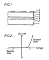
- Figure 1 is a diagram of a layered structure
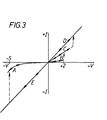
- Figure 2 and 3 depict the voltage/current characteristics of the structure before and after forming
- Figure 4 is plot of total thickness against forming voltage for a number of structures.
- ITO Indium Tin Oxide
- the chamber was evacuated to 10- 4 torr (1.3 x 10- 2 P a) and the substrate heated to 250°C. Pure silane gas was admitted to the chamber at a controlled continuous flow to bring the pressure to 0.1 torr (13 Pa). Once the system had stabilised a mixture of 1% by volume diborane in hydrogen gas was added to the silane to give a diborane/silane volume ratio of 10- 3 .
- a glow discharge was initiated by exciting a capacitive plate system inside the reaction chamber from a radio frequency generator. This caused p-type amorphous silicon containing boron to be deposited on the ITO coated glass from the gas phase.
- FIG. 1 The complete structure is shown in Figure 1 wherein 1 represents the glass substrate, 2 the layer of ITO, 3 the layer of p-type silicon, 4 the d-layer, 5 the layer of i-type 6 the layer of n-type and 7 the aluminium spots.
- the p-layer is about 200 A (20 nm) thick, the n-layer about 300 A (30 nm) and the i-layer about 1000 A (100 nm).
- the d-layer is estimated to be about 10 A (1 nm) thick on average, though this assumes the d-layer to be continuous and a growth rate equal to that observed for thicker films; in practice, however, the d-layer may be a discontinuous film of very variable thickness.
- the device was placed on a curve tracer and its voltage/current characteristics examined. Initially these were of the form shown in Figure 2. A reverse bias voltage of 2 volts was then applied to the device; this step "conditioned” the device into a memory (switching) device with characteristics as shown in Figure 3. The device is forward biased when 2 is more positive than 7.
- Curves A and B in Figure 3 show the device in its OFF state.
- Applying negative bias (curve A) has no effect on the conductivity state
- applying forward bias (curve B) causes the device to switch to an intermediate conductivity state (curve C) at about 2V.
- Further forward bias finally switches the device to its ON state, (curve D).
- Higher forward voltages have no further effect on the conductivity state for all values below that inducing breakdown by conventional means eg avalanche breakdown.
- Applying negative bias now leaves the device in the ON state (curve E) until a potential of 5V is attained, whereupon it immediately switches to its OFF state (curve A). This sequence of events is repeatable with no change in the ON-OFF conductivity or switching levels.
- the ON conductivity of the device was about 160 ohms, the OFF conductivity in excess of 500 K ohms, giving an ON-OFF ratio in excess of 3000.
- devices of the same thickness grown in the same manner without a d-layer have considerably higher forming voltages and ON-OFF ratios of only 30-100 as a result of a much higher conductivity OFF state. Additionally, the higher forming voltage often results in immediate destruction of the memory, thus successful forming is achieved on only 10% of devices, compared with almost 100% for structures including a d-layer.
- a device was prepared in a similar manner to Example 1, excepting that the ITO coated glass was deliberately placed in a region where non-uniform growth rates occurred due to plasma non-uniformity. This produced material with a range of thicknesses in all layers, onto which a pattern of aluminium dots was evaporated to give a series of devices of varying thickness.
Applications Claiming Priority (2)
| Application Number | Priority Date | Filing Date | Title |
|---|---|---|---|
| GB848400959A GB8400959D0 (en) | 1984-01-13 | 1984-01-13 | Semiconductor device |
| GB8400959 | 1984-01-13 |
Publications (2)
| Publication Number | Publication Date |
|---|---|
| EP0162529A1 true EP0162529A1 (de) | 1985-11-27 |
| EP0162529B1 EP0162529B1 (de) | 1989-03-01 |
Family
ID=10554971
Family Applications (1)
| Application Number | Title | Priority Date | Filing Date |
|---|---|---|---|
| EP85300039A Expired EP0162529B1 (de) | 1984-01-13 | 1985-01-03 | Amorphes oder mikrokristallines Halbleiterspeicherelement |
Country Status (6)
| Country | Link |
|---|---|
| US (1) | US4665428A (de) |
| EP (1) | EP0162529B1 (de) |
| JP (1) | JPS60220962A (de) |
| CA (1) | CA1220560A (de) |
| DE (1) | DE3568516D1 (de) |
| GB (1) | GB8400959D0 (de) |
Cited By (19)
| Publication number | Priority date | Publication date | Assignee | Title |
|---|---|---|---|---|
| EP0253201A3 (en) * | 1986-07-17 | 1990-01-03 | International Business Machines Corporation | Structure containing hydrogenated amorphous silicon and process |
| WO1990000817A1 (en) * | 1988-07-13 | 1990-01-25 | Raychem Limited | Electrical device |
| EP0483958A1 (de) * | 1990-10-26 | 1992-05-06 | Actel Corporation | Elektrisch-programmierbare Antischmelzsicherung mit einer dielektrischen Zwischenschicht und einer Zwischenschicht aus Amorphsilizium |
| US5360981A (en) * | 1989-05-11 | 1994-11-01 | British Telecommunications Public Limited Company | Amorphous silicon memory |
| US5477165A (en) * | 1986-09-19 | 1995-12-19 | Actel Corporation | Programmable logic module and architecture for field programmable gate array device |
| US5543656A (en) * | 1990-04-12 | 1996-08-06 | Actel Corporation | Metal to metal antifuse |
| US5552627A (en) * | 1990-04-12 | 1996-09-03 | Actel Corporation | Electrically programmable antifuse incorporating dielectric and amorphous silicon interlayers |
| US5565703A (en) * | 1993-10-18 | 1996-10-15 | Vlsi Technology, Inc. | Multi-level antifuse structure |
| US5570041A (en) * | 1986-09-19 | 1996-10-29 | Actel Corporation | Programmable logic module and architecture for field programmable gate array device |
| US5633189A (en) * | 1994-08-01 | 1997-05-27 | Actel Corporation | Method of making metal to metal antifuse |
| US5670818A (en) * | 1990-04-12 | 1997-09-23 | Actel Corporation | Electrically programmable antifuse |
| US5723358A (en) * | 1996-04-29 | 1998-03-03 | Vlsi Technology, Inc. | Method of manufacturing amorphous silicon antifuse structures |
| US5744980A (en) * | 1996-02-16 | 1998-04-28 | Actel Corporation | Flexible, high-performance static RAM architecture for field-programmable gate arrays |
| US5753540A (en) * | 1996-08-20 | 1998-05-19 | Vlsi Technology, Inc. | Apparatus and method for programming antifuse structures |
| US5763299A (en) * | 1995-06-06 | 1998-06-09 | Actel Corporation | Reduced leakage antifuse fabrication method |
| US5793094A (en) * | 1995-12-28 | 1998-08-11 | Vlsi Technology, Inc. | Methods for fabricating anti-fuse structures |
| US5804500A (en) * | 1995-06-02 | 1998-09-08 | Actel Corporation | Fabrication process for raised tungsten plug antifuse |
| US5882997A (en) * | 1996-09-30 | 1999-03-16 | Vlsi Technology, Inc. | Method for making devices having thin load structures |
| US6171512B1 (en) | 1991-02-15 | 2001-01-09 | Canon Kabushiki Kaisha | Etching solution for etching porous silicon, etching method using the etching solution and method of preparing semiconductor member using the etching solution |
Families Citing this family (29)
| Publication number | Priority date | Publication date | Assignee | Title |
|---|---|---|---|---|
| US4857982A (en) * | 1988-01-06 | 1989-08-15 | University Of Southern California | Avalanche photodiode with floating guard ring |
| US5311047A (en) * | 1988-11-16 | 1994-05-10 | National Science Council | Amorphous SI/SIC heterojunction color-sensitive phototransistor |
| US5614756A (en) | 1990-04-12 | 1997-03-25 | Actel Corporation | Metal-to-metal antifuse with conductive |
| US5780323A (en) | 1990-04-12 | 1998-07-14 | Actel Corporation | Fabrication method for metal-to-metal antifuses incorporating a tungsten via plug |
| US5909049A (en) | 1997-02-11 | 1999-06-01 | Actel Corporation | Antifuse programmed PROM cell |
| KR20010040487A (ko) * | 1998-02-02 | 2001-05-15 | 유니액스 코포레이션 | X-y 번지지정 가능한 전기 마이크로스위치 어레이 및이를 사용한 센서 매트릭스 |
| US8008700B2 (en) * | 2002-12-19 | 2011-08-30 | Sandisk 3D Llc | Non-volatile memory cell with embedded antifuse |
| US7285464B2 (en) | 2002-12-19 | 2007-10-23 | Sandisk 3D Llc | Nonvolatile memory cell comprising a reduced height vertical diode |
| US7800932B2 (en) | 2005-09-28 | 2010-09-21 | Sandisk 3D Llc | Memory cell comprising switchable semiconductor memory element with trimmable resistance |
| US7660181B2 (en) * | 2002-12-19 | 2010-02-09 | Sandisk 3D Llc | Method of making non-volatile memory cell with embedded antifuse |
| WO2004061851A2 (en) * | 2002-12-19 | 2004-07-22 | Matrix Semiconductor, Inc | An improved method for making high-density nonvolatile memory |
| US20070164388A1 (en) * | 2002-12-19 | 2007-07-19 | Sandisk 3D Llc | Memory cell comprising a diode fabricated in a low resistivity, programmed state |
| US20050226067A1 (en) | 2002-12-19 | 2005-10-13 | Matrix Semiconductor, Inc. | Nonvolatile memory cell operating by increasing order in polycrystalline semiconductor material |
| US8637366B2 (en) * | 2002-12-19 | 2014-01-28 | Sandisk 3D Llc | Nonvolatile memory cell without a dielectric antifuse having high- and low-impedance states |
| US7800933B2 (en) * | 2005-09-28 | 2010-09-21 | Sandisk 3D Llc | Method for using a memory cell comprising switchable semiconductor memory element with trimmable resistance |
| US7618850B2 (en) * | 2002-12-19 | 2009-11-17 | Sandisk 3D Llc | Method of making a diode read/write memory cell in a programmed state |
| US7307268B2 (en) * | 2005-01-19 | 2007-12-11 | Sandisk Corporation | Structure and method for biasing phase change memory array for reliable writing |
| US7800934B2 (en) * | 2005-09-28 | 2010-09-21 | Sandisk 3D Llc | Programming methods to increase window for reverse write 3D cell |
| US7684226B2 (en) * | 2007-06-25 | 2010-03-23 | Sandisk 3D Llc | Method of making high forward current diodes for reverse write 3D cell |
| US8102694B2 (en) * | 2007-06-25 | 2012-01-24 | Sandisk 3D Llc | Nonvolatile memory device containing carbon or nitrogen doped diode |
| US7830697B2 (en) * | 2007-06-25 | 2010-11-09 | Sandisk 3D Llc | High forward current diodes for reverse write 3D cell |
| US8072791B2 (en) * | 2007-06-25 | 2011-12-06 | Sandisk 3D Llc | Method of making nonvolatile memory device containing carbon or nitrogen doped diode |
| US7759666B2 (en) * | 2007-06-29 | 2010-07-20 | Sandisk 3D Llc | 3D R/W cell with reduced reverse leakage |
| US7800939B2 (en) * | 2007-06-29 | 2010-09-21 | Sandisk 3D Llc | Method of making 3D R/W cell with reduced reverse leakage |
| US7846782B2 (en) | 2007-09-28 | 2010-12-07 | Sandisk 3D Llc | Diode array and method of making thereof |
| US7830698B2 (en) * | 2008-04-11 | 2010-11-09 | Sandisk 3D Llc | Multilevel nonvolatile memory device containing a carbon storage material and methods of making and using same |
| US7812335B2 (en) * | 2008-04-11 | 2010-10-12 | Sandisk 3D Llc | Sidewall structured switchable resistor cell |
| US8450835B2 (en) * | 2008-04-29 | 2013-05-28 | Sandisk 3D Llc | Reverse leakage reduction and vertical height shrinking of diode with halo doping |
| US9806256B1 (en) | 2016-10-21 | 2017-10-31 | Sandisk Technologies Llc | Resistive memory device having sidewall spacer electrode and method of making thereof |
Citations (2)
| Publication number | Priority date | Publication date | Assignee | Title |
|---|---|---|---|---|
| FR2463508A1 (fr) * | 1979-08-16 | 1981-02-20 | Anvar | Procede de realisation de contacts ohmiques sur une couche active de silicium amorphe hydrogene |
| EP0095283A2 (de) * | 1982-05-15 | 1983-11-30 | The British Petroleum Company p.l.c. | Speicheranordnung |
Family Cites Families (2)
| Publication number | Priority date | Publication date | Assignee | Title |
|---|---|---|---|---|
| JPS5839070A (ja) * | 1981-08-31 | 1983-03-07 | Toshiba Corp | 半導体装置 |
| US4471155A (en) * | 1983-04-15 | 1984-09-11 | Energy Conversion Devices, Inc. | Narrow band gap photovoltaic devices with enhanced open circuit voltage |
-
1984
- 1984-01-13 GB GB848400959A patent/GB8400959D0/en active Pending
-
1985
- 1985-01-03 DE DE8585300039T patent/DE3568516D1/de not_active Expired
- 1985-01-03 EP EP85300039A patent/EP0162529B1/de not_active Expired
- 1985-01-11 CA CA000471941A patent/CA1220560A/en not_active Expired
- 1985-01-14 JP JP60004835A patent/JPS60220962A/ja active Pending
-
1986
- 1986-08-12 US US06/895,577 patent/US4665428A/en not_active Expired - Fee Related
Patent Citations (2)
| Publication number | Priority date | Publication date | Assignee | Title |
|---|---|---|---|---|
| FR2463508A1 (fr) * | 1979-08-16 | 1981-02-20 | Anvar | Procede de realisation de contacts ohmiques sur une couche active de silicium amorphe hydrogene |
| EP0095283A2 (de) * | 1982-05-15 | 1983-11-30 | The British Petroleum Company p.l.c. | Speicheranordnung |
Non-Patent Citations (1)
| Title |
|---|
| I.E.E. PROCEEDINGS, vol. 129, part I, no. 2, April 1982, Old Woking, GB; A.E. OWEN et al. "New amorphous-silicon electrically programmable nonvolatile switching device", pages 51-54 * |
Cited By (25)
| Publication number | Priority date | Publication date | Assignee | Title |
|---|---|---|---|---|
| EP0253201A3 (en) * | 1986-07-17 | 1990-01-03 | International Business Machines Corporation | Structure containing hydrogenated amorphous silicon and process |
| US5570041A (en) * | 1986-09-19 | 1996-10-29 | Actel Corporation | Programmable logic module and architecture for field programmable gate array device |
| US5606267A (en) * | 1986-09-19 | 1997-02-25 | Actel Corporation | Programmable logic module and architecture for field programmable gate array device |
| US5477165A (en) * | 1986-09-19 | 1995-12-19 | Actel Corporation | Programmable logic module and architecture for field programmable gate array device |
| WO1990000817A1 (en) * | 1988-07-13 | 1990-01-25 | Raychem Limited | Electrical device |
| US5151384A (en) * | 1988-07-13 | 1992-09-29 | Raychem Limited | Amorphous silicon switch with forming current controlled by contact region |
| US5360981A (en) * | 1989-05-11 | 1994-11-01 | British Telecommunications Public Limited Company | Amorphous silicon memory |
| US5770885A (en) * | 1990-04-12 | 1998-06-23 | Actel Corporation | Electrically programmable antifuse incorporating dielectric and amorphous silicon interlayers |
| US5543656A (en) * | 1990-04-12 | 1996-08-06 | Actel Corporation | Metal to metal antifuse |
| US5411917A (en) * | 1990-04-12 | 1995-05-02 | Actel Corporation | Electrically programmable antifuse incorporating dielectric and amorphous silicon interlayer |
| US5670818A (en) * | 1990-04-12 | 1997-09-23 | Actel Corporation | Electrically programmable antifuse |
| US5552627A (en) * | 1990-04-12 | 1996-09-03 | Actel Corporation | Electrically programmable antifuse incorporating dielectric and amorphous silicon interlayers |
| EP0483958A1 (de) * | 1990-10-26 | 1992-05-06 | Actel Corporation | Elektrisch-programmierbare Antischmelzsicherung mit einer dielektrischen Zwischenschicht und einer Zwischenschicht aus Amorphsilizium |
| US6171512B1 (en) | 1991-02-15 | 2001-01-09 | Canon Kabushiki Kaisha | Etching solution for etching porous silicon, etching method using the etching solution and method of preparing semiconductor member using the etching solution |
| US5565703A (en) * | 1993-10-18 | 1996-10-15 | Vlsi Technology, Inc. | Multi-level antifuse structure |
| US5633189A (en) * | 1994-08-01 | 1997-05-27 | Actel Corporation | Method of making metal to metal antifuse |
| US5804500A (en) * | 1995-06-02 | 1998-09-08 | Actel Corporation | Fabrication process for raised tungsten plug antifuse |
| US5763299A (en) * | 1995-06-06 | 1998-06-09 | Actel Corporation | Reduced leakage antifuse fabrication method |
| US5986322A (en) * | 1995-06-06 | 1999-11-16 | Mccollum; John L. | Reduced leakage antifuse structure |
| US5793094A (en) * | 1995-12-28 | 1998-08-11 | Vlsi Technology, Inc. | Methods for fabricating anti-fuse structures |
| US5744980A (en) * | 1996-02-16 | 1998-04-28 | Actel Corporation | Flexible, high-performance static RAM architecture for field-programmable gate arrays |
| US5962911A (en) * | 1996-04-29 | 1999-10-05 | Vlsi Technology, Inc. | Semiconductor devices having amorphous silicon antifuse structures |
| US5723358A (en) * | 1996-04-29 | 1998-03-03 | Vlsi Technology, Inc. | Method of manufacturing amorphous silicon antifuse structures |
| US5753540A (en) * | 1996-08-20 | 1998-05-19 | Vlsi Technology, Inc. | Apparatus and method for programming antifuse structures |
| US5882997A (en) * | 1996-09-30 | 1999-03-16 | Vlsi Technology, Inc. | Method for making devices having thin load structures |
Also Published As
| Publication number | Publication date |
|---|---|
| US4665428A (en) | 1987-05-12 |
| CA1220560A (en) | 1987-04-14 |
| GB8400959D0 (en) | 1984-02-15 |
| JPS60220962A (ja) | 1985-11-05 |
| DE3568516D1 (en) | 1989-04-06 |
| EP0162529B1 (de) | 1989-03-01 |
Similar Documents
| Publication | Publication Date | Title |
|---|---|---|
| EP0162529B1 (de) | Amorphes oder mikrokristallines Halbleiterspeicherelement | |
| US4251289A (en) | Gradient doping in amorphous silicon | |
| US4402762A (en) | Method of making highly stable modified amorphous silicon and germanium films | |
| US4385199A (en) | Photovoltaic cell having a hetero junction of amorphous silicon carbide and amorphous silicon | |
| GB2124826A (en) | Amorphous semiconductor materials | |
| CA1170786A (en) | Pin amorphous silicon semi-conductor device and method of manufacture | |
| JP2006080557A (ja) | 高水素希釈低温プラズマ蒸着によって製造されるアモルファスシリコン系素子の向上せしめられた安定化特性 | |
| EP0139487A1 (de) | Verfahren zum Beschichten einer amorphen pin- oder nip-Halbleiteranordnung mit teilweise kristallisierten p- und n-Schichten | |
| US4396793A (en) | Compensated amorphous silicon solar cell | |
| US4710786A (en) | Wide band gap semiconductor alloy material | |
| US4446168A (en) | Method of forming amorphous silicon | |
| US4508609A (en) | Method for sputtering a PIN microcrystalline/amorphous silicon semiconductor device with the P and N-layers sputtered from boron and phosphorous heavily doped targets | |
| GB2093271A (en) | Fabricating amorphous silicon solar cells | |
| EP0115124B1 (de) | Eine amorphe oder mikrokristalline Legierung enthaltende Speichereinrichtung | |
| US5358755A (en) | Amorphous hydrogenated silicon-carbon alloys and solar cells and other semiconductor devices produced therefrom | |
| KR100411897B1 (ko) | 반도체박막 및 박막 디바이스 | |
| JPS58210661A (ja) | 記憶デバイス | |
| WO1987002183A1 (en) | Multijunction semiconductor device | |
| JP2846639B2 (ja) | 非晶質太陽電池 | |
| JPH03101274A (ja) | アモルファス太陽電池の製造方法 | |
| JPH04286167A (ja) | 光起電力装置の製造方法 | |
| Walton et al. | Amorphous silicon/crystalline silicon heterojunctions for nuclear radiation detector applications | |
| Ro et al. | Microstructure and photovoltaic properties of low temperature polycrystalline silicon solar cells fabricated by VHF-GD CVD using fluorinated gas | |
| JPH02177371A (ja) | アモルファス太陽電池の製造方法 | |
| JPS63244888A (ja) | 半導体装置 |
Legal Events
| Date | Code | Title | Description |
|---|---|---|---|
| PUAI | Public reference made under article 153(3) epc to a published international application that has entered the european phase |
Free format text: ORIGINAL CODE: 0009012 |
|
| AK | Designated contracting states |
Designated state(s): BE DE FR GB IT NL |
|
| 17P | Request for examination filed |
Effective date: 19860415 |
|
| 17Q | First examination report despatched |
Effective date: 19880322 |
|
| GRAA | (expected) grant |
Free format text: ORIGINAL CODE: 0009210 |
|
| AK | Designated contracting states |
Kind code of ref document: B1 Designated state(s): BE DE FR GB IT NL |
|
| ITF | It: translation for a ep patent filed | ||
| REF | Corresponds to: |
Ref document number: 3568516 Country of ref document: DE Date of ref document: 19890406 |
|
| ET | Fr: translation filed | ||
| PGFP | Annual fee paid to national office [announced via postgrant information from national office to epo] |
Ref country code: FR Payment date: 19891009 Year of fee payment: 6 |
|
| PGFP | Annual fee paid to national office [announced via postgrant information from national office to epo] |
Ref country code: DE Payment date: 19891109 Year of fee payment: 6 |
|
| PGFP | Annual fee paid to national office [announced via postgrant information from national office to epo] |
Ref country code: GB Payment date: 19891231 Year of fee payment: 6 |
|
| PLBE | No opposition filed within time limit |
Free format text: ORIGINAL CODE: 0009261 |
|
| STAA | Information on the status of an ep patent application or granted ep patent |
Free format text: STATUS: NO OPPOSITION FILED WITHIN TIME LIMIT |
|
| ITTA | It: last paid annual fee | ||
| PGFP | Annual fee paid to national office [announced via postgrant information from national office to epo] |
Ref country code: NL Payment date: 19900131 Year of fee payment: 6 |
|
| PGFP | Annual fee paid to national office [announced via postgrant information from national office to epo] |
Ref country code: BE Payment date: 19900213 Year of fee payment: 6 |
|
| 26N | No opposition filed | ||
| PG25 | Lapsed in a contracting state [announced via postgrant information from national office to epo] |
Ref country code: GB Effective date: 19910103 |
|
| PG25 | Lapsed in a contracting state [announced via postgrant information from national office to epo] |
Ref country code: BE Effective date: 19910131 |
|
| PG25 | Lapsed in a contracting state [announced via postgrant information from national office to epo] |
Ref country code: NL Effective date: 19910801 |
|
| GBPC | Gb: european patent ceased through non-payment of renewal fee | ||
| NLV4 | Nl: lapsed or anulled due to non-payment of the annual fee | ||
| PG25 | Lapsed in a contracting state [announced via postgrant information from national office to epo] |
Ref country code: FR Effective date: 19910930 |
|
| PG25 | Lapsed in a contracting state [announced via postgrant information from national office to epo] |
Ref country code: DE Effective date: 19911001 |
|
| REG | Reference to a national code |
Ref country code: FR Ref legal event code: ST |