EP0159654A2 - Circuit amplificateur - Google Patents
Circuit amplificateur Download PDFInfo
- Publication number
- EP0159654A2 EP0159654A2 EP85104580A EP85104580A EP0159654A2 EP 0159654 A2 EP0159654 A2 EP 0159654A2 EP 85104580 A EP85104580 A EP 85104580A EP 85104580 A EP85104580 A EP 85104580A EP 0159654 A2 EP0159654 A2 EP 0159654A2
- Authority
- EP
- European Patent Office
- Prior art keywords
- transistors
- power source
- channel mos
- transistor
- mos transistors
- Prior art date
- Legal status (The legal status is an assumption and is not a legal conclusion. Google has not performed a legal analysis and makes no representation as to the accuracy of the status listed.)
- Granted
Links
Images

Classifications
-
- H—ELECTRICITY
- H03—ELECTRONIC CIRCUITRY
- H03F—AMPLIFIERS
- H03F3/00—Amplifiers with only discharge tubes or only semiconductor devices as amplifying elements
- H03F3/45—Differential amplifiers
- H03F3/45071—Differential amplifiers with semiconductor devices only
- H03F3/45076—Differential amplifiers with semiconductor devices only characterised by the way of implementation of the active amplifying circuit in the differential amplifier
-
- H—ELECTRICITY
- H03—ELECTRONIC CIRCUITRY
- H03F—AMPLIFIERS
- H03F1/00—Details of amplifiers with only discharge tubes, only semiconductor devices or only unspecified devices as amplifying elements
- H03F1/08—Modifications of amplifiers to reduce detrimental influences of internal impedances of amplifying elements
- H03F1/22—Modifications of amplifiers to reduce detrimental influences of internal impedances of amplifying elements by use of cascode coupling, i.e. earthed cathode or emitter stage followed by earthed grid or base stage respectively
- H03F1/223—Modifications of amplifiers to reduce detrimental influences of internal impedances of amplifying elements by use of cascode coupling, i.e. earthed cathode or emitter stage followed by earthed grid or base stage respectively with MOSFET's
Definitions
- This invention relates to an amplifier circuit and, more particularly, to an amplifier circuit with a small input current which usually involves a noise problem in low frequencies of the input signal.
- N channel MOS transistors Ml and M2 form a differential amplifier.
- Vl and V2 designate power sources with differential terminal voltages + Vin/2 and - Vin/2, respectively.
- 10 designates a bias power source for the power sources V1 and V2.
- An input signal Sl at a differential potential Vin is applied between the gates Gl and G2 of the transistors Gl and G2.
- Reference numeral 11 designates a current source, and Zl and Z2 denote loads.
- Numeral 12 is representative of a power line connected to a high potential Vcc. GND denotes ground.
- the output voltage Vout of this circuit is derived from the drains of the MOS transistors Ml and M2.
- PNP bipolar transistors Ql and Q2 form a differential amplifier.
- An input signal Sl is applied between the bases Bl and B2 of these transistors Ql and Q2.
- Emitters of the transistors Ql and Q2 are connected in series to transistors Q3 and Q4, respectively.
- the output voltage Vout is derived from the collectors of the transistors Q3 and Q4.
- a bias source 13 is provided for the transistors Q3 and Q4.
- the N channel MOS transistors Ml and M2 are used as input elements.
- the noise power i.e., 1/f noise
- the N channel MOS transistor causes noise approximately three times the P channel one. Therefore, the Fig. 1 circuit of prior art using the N channel transistor is inappropriate for use in the amplifier operating in audio frequencies.
- the PNP bipolar transistors Q1 and Q2 are used as the input elements.
- the base current flow inevitably . and adversely influences the input signal, particularly when the input current is small.
- the pair of PNP transistors Ql and Q2, and the pair of NPN transistors Q3 and Q4 are each connected in a complimentary fashion.
- the object of this invention is to provide an amplifier circuit which realizes a reduction in the noise caused by the input transistor, improves the frequency response, and produces a stable output signal for a small input current applied.
- P channel MOS transistors are used for the input elements.
- the sources of these transistors are connected to the emitters of bipolar transistors Qll and Q12. With this arrangement, the input current is negligible, the frequency response is improved, and the noise proper to the input elements is improved.
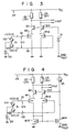
- Fig. 3 illustrating a first embodiment of an amplifier circuit according to the present invention.
- a pair of P channel MOS transistors Mll and M12 form a differential amplifier.
- V21 and V22 designate differential power sources of terminal voltages + Vin/2 and - Vin/2, respectively.
- a junction between the power sources V21 and V22 is connected to a positive terminal of a bias power source 20.
- a negative terminal of the power source 20 is connected to ground GND.
- An input signal Sl at a potential Vin is connected between the gates Gl and G2 of the MOS transistors Mll and M12.
- the drains of the transistors M11 and M12 are connected to a lower potential VEE (in this embodiment, it is ground potential GND).
- the sources of the NPN bipolar transistors M11 and M12 are connected to the emitters of NPN bipolar transistors Qll and Q12, respectively.
- the bases of the bipolar transistors Qll and Q12 are connected together to the positive terminal of the bias power source 21.
- the collectors of these transistors are connected through loads 22 and 23 to a power line 24 coupled with a high potential Vcc.
- the potential VEE and Vcc constitute a pair of power source potentials.
- the negative terminal of the bias power source 21 is connected to ground GND.
- the output signal Vout of this circuit is derived from the collectors of the bipolar transistors Qll and Q12.
- the source potentials of the MOS transistors Mll and 12 are substantially constant.
- the current flowing into the transistors M11 and M12 are gmVin if the voltage - current converting coefficient is gm.
- the output voltage Vo is gmzoVin, and the voltage gain vo/vi is gmzo.
- the output voltage Vout is Vout
- VTH is the threshold voltage of each transistor M11 and M12.
- VGSO is a DC bias voltage between the gate and the source of each transistor M11 and M12.
- the equation (3) shows that the Fig. 3 circuit can obtain an amplified output voltage proportional to the input signal.
- a bias power source circuit for biasing the NPN transistors Qll and Q12 is composed of N channel MOS transistors M13 and M14, and a constant current source 25.
- the remaining circuit arrangement is the same as that of the Fig. 3 circuit.
- the pair of transistors M13 and M14 provide a current mirror circuit.
- the MOS transistor M13 is connected between the source of the MOS transistor Mll and ground.
- the drain of the transistor M13 is connected to the drain of the transistor Mll. Its source is connected to ground GND.
- the constant current source 25 and the transistor M11 are connected in series between the power line 24 and ground GND.
- the constant current source 25 is connected to the power line 24.
- the transistor M14 is connected to ground.
- the constant current source 25 is connected at the input to the power line 24, and at the output to the drain of the transistor M14.
- the junction between the drain of the transistor M14 and the power source 25 is connected to the base of the transistor Q12.
- the source of the transistor M14 is connected to ground GND.
- the gates of the MOS transistors M13 and M14 are connected together to the drain of the transistor M12.
- the gate of the transistor M13 is connected to its drain.
- the drains of the transistors Mll and M12 serve as input terminals. In the Fig. 4 circuit, unlike the Fig. 3 circuit, it is not connected to ground GND.
- the bias circuit thus arranged is of the negative feedback type.
- the current mirror composed of the transistors M13 and M14 operates to decreases the base potential of the transistor Qll and to restrict the large current. Therefore, a further stabilized operation of the amplifier circuit is ensured.
- the input elements are P channel MOS transistors M11 and M12.
- the 1/f noise of this type of transistor is lower than that of the P channel type MOS transistor. Therefore, if the input signal has a small amplitude and a low frequency, a lower noise is generated and therefore a high quality amplified signal can be obtained. Additionally, this type of transistor is free from the base current flow, unlike the bipolar transistor. Therefore, the adverse influence by the base current flow on the input current can be removed.
- the source of the P channel MOS transistor Mll is connected to the emitter of the transistor Qll or the source of the P channel MOS transistor M12 is connected to the emitter of the transistor Q12. That is to say, this circuit connection provides a cascode amplifier. Therefore, the gate-source capacitance of each transistor Mll and M12 is extremely small, and the emitter resistance of each transistor is small. The time constant, as defined by the capacitance and resistance, is small. This implies that no mirror capacitance is present, and the frequency response in high frequencies is improved, and therefore the amplifier circuit of the present invention has a good broad band characteristic. In the Fig. 4 circuit arrangement, the P channel MOS transistors and the N channel transistors are combined. This feature provides a preferable sequence of the manufacturing steps when the CMOS-bipolar hybrid technique is used for the IC fabrication. Therefore, effective manufacturing of the amplifier circuits can be realized.
Applications Claiming Priority (2)
| Application Number | Priority Date | Filing Date | Title |
|---|---|---|---|
| JP85020/84 | 1984-04-26 | ||
| JP59085020A JPS60229404A (ja) | 1984-04-26 | 1984-04-26 | 増幅回路 |
Publications (3)
| Publication Number | Publication Date |
|---|---|
| EP0159654A2 true EP0159654A2 (fr) | 1985-10-30 |
| EP0159654A3 EP0159654A3 (en) | 1987-01-07 |
| EP0159654B1 EP0159654B1 (fr) | 1991-01-30 |
Family
ID=13847046
Family Applications (1)
| Application Number | Title | Priority Date | Filing Date |
|---|---|---|---|
| EP85104580A Expired EP0159654B1 (fr) | 1984-04-26 | 1985-04-16 | Circuit amplificateur |
Country Status (4)
| Country | Link |
|---|---|
| US (1) | US4626794A (fr) |
| EP (1) | EP0159654B1 (fr) |
| JP (1) | JPS60229404A (fr) |
| DE (1) | DE3581553D1 (fr) |
Cited By (5)
| Publication number | Priority date | Publication date | Assignee | Title |
|---|---|---|---|---|
| WO1986007215A1 (fr) * | 1985-05-28 | 1986-12-04 | Wolfson Microelectronics Limited | Ameliorations relatives a des transconducteurs |
| EP0284092A2 (fr) * | 1987-03-27 | 1988-09-28 | Kabushiki Kaisha Toshiba | Amplificateur différentiel |
| GB2280999A (en) * | 1993-08-09 | 1995-02-15 | Motorola Inc | Transconductance amplifiers |
| DE4329639A1 (de) * | 1993-09-02 | 1995-03-09 | Telefunken Microelectron | Schaltungsanordnung mit gesteuerten Pinch-Widerständen |
| WO1998024176A1 (fr) * | 1996-11-29 | 1998-06-04 | Varian Associates, Inc. | Amplificateur reagissant a la charge et capable d'un taux eleve d'elimination du signal en mode commun |
Families Citing this family (15)
| Publication number | Priority date | Publication date | Assignee | Title |
|---|---|---|---|---|
| JPS62154287A (ja) * | 1985-12-27 | 1987-07-09 | Hitachi Ltd | 半導体メモリ装置 |
| IT1252392B (it) * | 1991-11-13 | 1995-06-12 | Sgs Thomson Microelectronics | Stadio transconduttore perfezionato per filtri ad alta frequenza |
| US5304869A (en) * | 1992-04-17 | 1994-04-19 | Intel Corporation | BiCMOS digital amplifier |
| FR2699763B1 (fr) * | 1992-12-22 | 1995-01-20 | Matra Communication | Amplificateur à transconductance. |
| US5760647A (en) * | 1996-06-04 | 1998-06-02 | Motorola, Inc. | High bandwidth fast settling time operational amplifier and method therefor |
| US6504433B1 (en) * | 2000-09-15 | 2003-01-07 | Atheros Communications, Inc. | CMOS transceiver having an integrated power amplifier |
| JP2003110380A (ja) * | 2001-06-26 | 2003-04-11 | Koninkl Philips Electronics Nv | 大出力電流増幅器 |
| WO2003003561A1 (fr) * | 2001-06-29 | 2003-01-09 | Niigata Seimitsu Co., Ltd. | Circuit melangeur de frequences |
| JP2003283271A (ja) | 2002-01-17 | 2003-10-03 | Semiconductor Energy Lab Co Ltd | 電気回路 |
| JP2004040735A (ja) * | 2002-07-08 | 2004-02-05 | Toyota Industries Corp | 半導体集積回路及び半導体集積回路の製造方法 |
| US6958651B2 (en) | 2002-12-03 | 2005-10-25 | Semiconductor Energy Laboratory Co., Ltd. | Analog circuit and display device using the same |
| US7589326B2 (en) | 2003-10-15 | 2009-09-15 | Varian Medical Systems Technologies, Inc. | Systems and methods for image acquisition |
| US7095028B2 (en) | 2003-10-15 | 2006-08-22 | Varian Medical Systems | Multi-slice flat panel computed tomography |
| JP2009111724A (ja) * | 2007-10-30 | 2009-05-21 | Nec Electronics Corp | 増幅器 |
| JP2008125134A (ja) * | 2008-02-12 | 2008-05-29 | Seiko Epson Corp | 半導体装置 |
Citations (1)
| Publication number | Priority date | Publication date | Assignee | Title |
|---|---|---|---|---|
| US4390850A (en) * | 1981-03-16 | 1983-06-28 | Motorola, Inc. | Operational amplifier having improved slew rate/bandwidth characteristics |
Family Cites Families (3)
| Publication number | Priority date | Publication date | Assignee | Title |
|---|---|---|---|---|
| US4004245A (en) * | 1976-05-03 | 1977-01-18 | National Semiconductor Corporation | Wide common mode range differential amplifier |
| JPS5360546A (en) * | 1976-11-12 | 1978-05-31 | Hitachi Ltd | Amplifier |
| US4387309A (en) * | 1981-07-06 | 1983-06-07 | Motorola, Inc. | Input stage for N-channel junction field effect transistor operational amplifier |
-
1984
- 1984-04-26 JP JP59085020A patent/JPS60229404A/ja active Granted
-
1985
- 1985-04-16 EP EP85104580A patent/EP0159654B1/fr not_active Expired
- 1985-04-16 DE DE8585104580T patent/DE3581553D1/de not_active Expired - Lifetime
- 1985-04-23 US US06/726,349 patent/US4626794A/en not_active Expired - Lifetime
Patent Citations (1)
| Publication number | Priority date | Publication date | Assignee | Title |
|---|---|---|---|---|
| US4390850A (en) * | 1981-03-16 | 1983-06-28 | Motorola, Inc. | Operational amplifier having improved slew rate/bandwidth characteristics |
Non-Patent Citations (2)
| Title |
|---|
| IEEE JOURNAL OF SOLID-STATE CIRCUITS, vol. SC-13, no. 6, December 1978, pages 799-805, IEEE, New York, US; W. STEINHAGEN et al.: "Design of integrated analog CMOS circuits - A multichannel telemetry transmitter" * |
| MEASUREMENT TECHNIQUES, vol. 19, no. 9, September 1976, pages 1313,1314; D.E. POLONNIKOV et al.: "Electrometer amplifier using MOS transistors" * |
Cited By (9)
| Publication number | Priority date | Publication date | Assignee | Title |
|---|---|---|---|---|
| WO1986007215A1 (fr) * | 1985-05-28 | 1986-12-04 | Wolfson Microelectronics Limited | Ameliorations relatives a des transconducteurs |
| US4823092A (en) * | 1985-05-28 | 1989-04-18 | Wolfson Microelectronics Limited | MOS transconductance amplifier for active filters |
| EP0284092A2 (fr) * | 1987-03-27 | 1988-09-28 | Kabushiki Kaisha Toshiba | Amplificateur différentiel |
| EP0284092A3 (fr) * | 1987-03-27 | 1989-06-07 | Kabushiki Kaisha Toshiba | Amplificateur différentiel |
| GB2280999A (en) * | 1993-08-09 | 1995-02-15 | Motorola Inc | Transconductance amplifiers |
| DE4329639A1 (de) * | 1993-09-02 | 1995-03-09 | Telefunken Microelectron | Schaltungsanordnung mit gesteuerten Pinch-Widerständen |
| US5451908A (en) * | 1993-09-02 | 1995-09-19 | Temic Telefunken Microelectronic Gmbh | Circuit arrangement with controlled pinch resistors |
| WO1998024176A1 (fr) * | 1996-11-29 | 1998-06-04 | Varian Associates, Inc. | Amplificateur reagissant a la charge et capable d'un taux eleve d'elimination du signal en mode commun |
| US6084461A (en) * | 1996-11-29 | 2000-07-04 | Varian Medical Systems, Inc. | Charge sensitive amplifier with high common mode signal rejection |
Also Published As
| Publication number | Publication date |
|---|---|
| EP0159654B1 (fr) | 1991-01-30 |
| EP0159654A3 (en) | 1987-01-07 |
| DE3581553D1 (de) | 1991-03-07 |
| JPS60229404A (ja) | 1985-11-14 |
| US4626794A (en) | 1986-12-02 |
| JPH0582082B2 (fr) | 1993-11-17 |
Similar Documents
| Publication | Publication Date | Title |
|---|---|---|
| EP0159654A2 (fr) | Circuit amplificateur | |
| US4048575A (en) | Operational amplifier | |
| US5734296A (en) | Low voltage operational amplifier input stage and method | |
| US5699015A (en) | Low voltage operational amplifier and method | |
| US5608352A (en) | Differential input circuit capable of broadening operation range of input common mode potential | |
| US8138839B2 (en) | Wideband CMOS gain stage | |
| US5798673A (en) | Low voltage operational amplifier bias circuit and method | |
| US4524329A (en) | Operational amplifier circuit | |
| US5028881A (en) | Highly linear operational transconductance amplifier with low transconductance | |
| EP0448951A2 (fr) | Amplificateur à faible bruit et a haute impédance d'entrée, en particulier pour microphones | |
| US3956708A (en) | MOSFET comparator | |
| KR0140160B1 (ko) | 저동작전압에서 작동이 가능하고, 고출력 임피던스를 갖는 캐스코드 회로 | |
| EP0240830A2 (fr) | Circuit comparateur de tension | |
| KR900008159B1 (ko) | 차동증폭기 | |
| US6545502B1 (en) | High frequency MOS fixed and variable gain amplifiers | |
| US20060139096A1 (en) | Apparatus and method for biasing cascode devices in a differential pair using the input, output, or other nodes in the circuit | |
| US6788143B1 (en) | Cascode stage for an operational amplifier | |
| US6072339A (en) | Current sensing circuit with high input impedance | |
| JPH06196948A (ja) | 相互コンダクタ段 | |
| JP3081210B2 (ja) | 線形利得増幅回路 | |
| KR100203965B1 (ko) | 반도체 집적회로 | |
| US20020163386A1 (en) | Amplifying circuit | |
| US4060770A (en) | Differential amplifier | |
| CA1180773A (fr) | Amplificateur differentiel avec conversion de la sortie differentielle en sortie simple | |
| US5049833A (en) | Amplifier stage |
Legal Events
| Date | Code | Title | Description |
|---|---|---|---|
| PUAI | Public reference made under article 153(3) epc to a published international application that has entered the european phase |
Free format text: ORIGINAL CODE: 0009012 |
|
| 17P | Request for examination filed |
Effective date: 19850513 |
|
| AK | Designated contracting states |
Designated state(s): DE FR GB IT |
|
| PUAL | Search report despatched |
Free format text: ORIGINAL CODE: 0009013 |
|
| AK | Designated contracting states |
Kind code of ref document: A3 Designated state(s): DE FR GB IT |
|
| 17Q | First examination report despatched |
Effective date: 19890228 |
|
| GRAA | (expected) grant |
Free format text: ORIGINAL CODE: 0009210 |
|
| AK | Designated contracting states |
Kind code of ref document: B1 Designated state(s): DE FR GB IT |
|
| ITF | It: translation for a ep patent filed |
Owner name: JACOBACCI & PERANI S.P.A. |
|
| ET | Fr: translation filed | ||
| REF | Corresponds to: |
Ref document number: 3581553 Country of ref document: DE Date of ref document: 19910307 |
|
| PLBE | No opposition filed within time limit |
Free format text: ORIGINAL CODE: 0009261 |
|
| STAA | Information on the status of an ep patent application or granted ep patent |
Free format text: STATUS: NO OPPOSITION FILED WITHIN TIME LIMIT |
|
| 26N | No opposition filed | ||
| PGFP | Annual fee paid to national office [announced via postgrant information from national office to epo] |
Ref country code: GB Payment date: 19980407 Year of fee payment: 14 |
|
| PGFP | Annual fee paid to national office [announced via postgrant information from national office to epo] |
Ref country code: FR Payment date: 19980409 Year of fee payment: 14 |
|
| PGFP | Annual fee paid to national office [announced via postgrant information from national office to epo] |
Ref country code: DE Payment date: 19980424 Year of fee payment: 14 |
|
| PG25 | Lapsed in a contracting state [announced via postgrant information from national office to epo] |
Ref country code: GB Free format text: LAPSE BECAUSE OF NON-PAYMENT OF DUE FEES Effective date: 19990416 |
|
| GBPC | Gb: european patent ceased through non-payment of renewal fee |
Effective date: 19990416 |
|
| PG25 | Lapsed in a contracting state [announced via postgrant information from national office to epo] |
Ref country code: FR Free format text: LAPSE BECAUSE OF NON-PAYMENT OF DUE FEES Effective date: 19991231 |
|
| REG | Reference to a national code |
Ref country code: FR Ref legal event code: ST |
|
| PG25 | Lapsed in a contracting state [announced via postgrant information from national office to epo] |
Ref country code: DE Free format text: LAPSE BECAUSE OF NON-PAYMENT OF DUE FEES Effective date: 20000201 |