EP0159544A1 - Avalanche photodiode and its manufacturing method - Google Patents
Avalanche photodiode and its manufacturing method Download PDFInfo
- Publication number
- EP0159544A1 EP0159544A1 EP85103299A EP85103299A EP0159544A1 EP 0159544 A1 EP0159544 A1 EP 0159544A1 EP 85103299 A EP85103299 A EP 85103299A EP 85103299 A EP85103299 A EP 85103299A EP 0159544 A1 EP0159544 A1 EP 0159544A1
- Authority
- EP
- European Patent Office
- Prior art keywords
- junction
- semiconductor layer
- avalanche
- periphery
- graded
- Prior art date
- Legal status (The legal status is an assumption and is not a legal conclusion. Google has not performed a legal analysis and makes no representation as to the accuracy of the status listed.)
- Granted
Links
- 238000004519 manufacturing process Methods 0.000 title claims description 13
- 239000004065 semiconductor Substances 0.000 claims abstract description 30
- 229910001423 beryllium ion Inorganic materials 0.000 claims description 17
- 238000000034 method Methods 0.000 claims description 14
- 238000005468 ion implantation Methods 0.000 claims description 8
- 238000007669 thermal treatment Methods 0.000 claims description 8
- 230000004913 activation Effects 0.000 claims description 5
- 230000015556 catabolic process Effects 0.000 abstract description 26
- 239000010408 film Substances 0.000 description 20
- 229910000530 Gallium indium arsenide Inorganic materials 0.000 description 16
- VYPSYNLAJGMNEJ-UHFFFAOYSA-N Silicium dioxide Chemical compound O=[Si]=O VYPSYNLAJGMNEJ-UHFFFAOYSA-N 0.000 description 15
- 229910052681 coesite Inorganic materials 0.000 description 9
- 229910052906 cristobalite Inorganic materials 0.000 description 9
- 238000009826 distribution Methods 0.000 description 9
- 230000002093 peripheral effect Effects 0.000 description 9
- 229910052682 stishovite Inorganic materials 0.000 description 9
- 229910052905 tridymite Inorganic materials 0.000 description 9
- 239000000758 substrate Substances 0.000 description 8
- KRHYYFGTRYWZRS-UHFFFAOYSA-N Fluorane Chemical compound F KRHYYFGTRYWZRS-UHFFFAOYSA-N 0.000 description 7
- 238000005229 chemical vapour deposition Methods 0.000 description 7
- 238000005530 etching Methods 0.000 description 7
- 229960002050 hydrofluoric acid Drugs 0.000 description 7
- 150000002500 ions Chemical class 0.000 description 7
- 239000000377 silicon dioxide Substances 0.000 description 6
- 230000015572 biosynthetic process Effects 0.000 description 5
- 238000009792 diffusion process Methods 0.000 description 5
- 230000000694 effects Effects 0.000 description 5
- 239000012535 impurity Substances 0.000 description 5
- 230000008569 process Effects 0.000 description 5
- 230000035945 sensitivity Effects 0.000 description 5
- 238000002161 passivation Methods 0.000 description 4
- 230000008901 benefit Effects 0.000 description 3
- 229910052790 beryllium Inorganic materials 0.000 description 3
- ATBAMAFKBVZNFJ-UHFFFAOYSA-N beryllium atom Chemical compound [Be] ATBAMAFKBVZNFJ-UHFFFAOYSA-N 0.000 description 3
- 238000007687 exposure technique Methods 0.000 description 3
- 238000002513 implantation Methods 0.000 description 3
- 229910000980 Aluminium gallium arsenide Inorganic materials 0.000 description 2
- QAOWNCQODCNURD-UHFFFAOYSA-N Sulfuric acid Chemical compound OS(O)(=O)=O QAOWNCQODCNURD-UHFFFAOYSA-N 0.000 description 2
- PWOSZCQLSAMRQW-UHFFFAOYSA-N beryllium(2+) Chemical compound [Be+2] PWOSZCQLSAMRQW-UHFFFAOYSA-N 0.000 description 2
- 239000013078 crystal Substances 0.000 description 2
- 230000005684 electric field Effects 0.000 description 2
- 239000000203 mixture Substances 0.000 description 2
- 230000003287 optical effect Effects 0.000 description 2
- BASFCYQUMIYNBI-UHFFFAOYSA-N platinum Chemical compound [Pt] BASFCYQUMIYNBI-UHFFFAOYSA-N 0.000 description 2
- 238000007363 ring formation reaction Methods 0.000 description 2
- 238000009834 vaporization Methods 0.000 description 2
- 108091006149 Electron carriers Proteins 0.000 description 1
- 229910005542 GaSb Inorganic materials 0.000 description 1
- 229910001218 Gallium arsenide Inorganic materials 0.000 description 1
- 229910000990 Ni alloy Inorganic materials 0.000 description 1
- 229910004298 SiO 2 Inorganic materials 0.000 description 1
- RTAQQCXQSZGOHL-UHFFFAOYSA-N Titanium Chemical group [Ti] RTAQQCXQSZGOHL-UHFFFAOYSA-N 0.000 description 1
- 230000005540 biological transmission Effects 0.000 description 1
- 229910052793 cadmium Inorganic materials 0.000 description 1
- BDOSMKKIYDKNTQ-UHFFFAOYSA-N cadmium atom Chemical compound [Cd] BDOSMKKIYDKNTQ-UHFFFAOYSA-N 0.000 description 1
- 230000008859 change Effects 0.000 description 1
- 239000002131 composite material Substances 0.000 description 1
- 150000001875 compounds Chemical class 0.000 description 1
- 239000012141 concentrate Substances 0.000 description 1
- 230000007547 defect Effects 0.000 description 1
- 238000000151 deposition Methods 0.000 description 1
- 230000008021 deposition Effects 0.000 description 1
- 230000009977 dual effect Effects 0.000 description 1
- 230000005284 excitation Effects 0.000 description 1
- PCHJSUWPFVWCPO-UHFFFAOYSA-N gold Chemical compound [Au] PCHJSUWPFVWCPO-UHFFFAOYSA-N 0.000 description 1
- 229910052737 gold Inorganic materials 0.000 description 1
- 239000010931 gold Substances 0.000 description 1
- 238000010438 heat treatment Methods 0.000 description 1
- 150000004678 hydrides Chemical class 0.000 description 1
- 230000006872 improvement Effects 0.000 description 1
- 239000013307 optical fiber Substances 0.000 description 1
- 238000000623 plasma-assisted chemical vapour deposition Methods 0.000 description 1
- 229910052697 platinum Inorganic materials 0.000 description 1
- 230000009467 reduction Effects 0.000 description 1
- 239000005368 silicate glass Substances 0.000 description 1
- 239000010409 thin film Substances 0.000 description 1
- 229910052719 titanium Inorganic materials 0.000 description 1
- 239000010936 titanium Substances 0.000 description 1
- 238000000927 vapour-phase epitaxy Methods 0.000 description 1
- 235000012431 wafers Nutrition 0.000 description 1
Images


Classifications
-
- H—ELECTRICITY
- H01—ELECTRIC ELEMENTS
- H01L—SEMICONDUCTOR DEVICES NOT COVERED BY CLASS H10
- H01L29/00—Semiconductor devices adapted for rectifying, amplifying, oscillating or switching, or capacitors or resistors with at least one potential-jump barrier or surface barrier, e.g. PN junction depletion layer or carrier concentration layer; Details of semiconductor bodies or of electrodes thereof ; Multistep manufacturing processes therefor
- H01L29/02—Semiconductor bodies ; Multistep manufacturing processes therefor
- H01L29/06—Semiconductor bodies ; Multistep manufacturing processes therefor characterised by their shape; characterised by the shapes, relative sizes, or dispositions of the semiconductor regions ; characterised by the concentration or distribution of impurities within semiconductor regions
- H01L29/0603—Semiconductor bodies ; Multistep manufacturing processes therefor characterised by their shape; characterised by the shapes, relative sizes, or dispositions of the semiconductor regions ; characterised by the concentration or distribution of impurities within semiconductor regions characterised by particular constructional design considerations, e.g. for preventing surface leakage, for controlling electric field concentration or for internal isolations regions
- H01L29/0607—Semiconductor bodies ; Multistep manufacturing processes therefor characterised by their shape; characterised by the shapes, relative sizes, or dispositions of the semiconductor regions ; characterised by the concentration or distribution of impurities within semiconductor regions characterised by particular constructional design considerations, e.g. for preventing surface leakage, for controlling electric field concentration or for internal isolations regions for preventing surface leakage or controlling electric field concentration
- H01L29/0611—Semiconductor bodies ; Multistep manufacturing processes therefor characterised by their shape; characterised by the shapes, relative sizes, or dispositions of the semiconductor regions ; characterised by the concentration or distribution of impurities within semiconductor regions characterised by particular constructional design considerations, e.g. for preventing surface leakage, for controlling electric field concentration or for internal isolations regions for preventing surface leakage or controlling electric field concentration for increasing or controlling the breakdown voltage of reverse biased devices
- H01L29/0615—Semiconductor bodies ; Multistep manufacturing processes therefor characterised by their shape; characterised by the shapes, relative sizes, or dispositions of the semiconductor regions ; characterised by the concentration or distribution of impurities within semiconductor regions characterised by particular constructional design considerations, e.g. for preventing surface leakage, for controlling electric field concentration or for internal isolations regions for preventing surface leakage or controlling electric field concentration for increasing or controlling the breakdown voltage of reverse biased devices by the doping profile or the shape or the arrangement of the PN junction, or with supplementary regions, e.g. junction termination extension [JTE]
- H01L29/0619—Semiconductor bodies ; Multistep manufacturing processes therefor characterised by their shape; characterised by the shapes, relative sizes, or dispositions of the semiconductor regions ; characterised by the concentration or distribution of impurities within semiconductor regions characterised by particular constructional design considerations, e.g. for preventing surface leakage, for controlling electric field concentration or for internal isolations regions for preventing surface leakage or controlling electric field concentration for increasing or controlling the breakdown voltage of reverse biased devices by the doping profile or the shape or the arrangement of the PN junction, or with supplementary regions, e.g. junction termination extension [JTE] with a supplementary region doped oppositely to or in rectifying contact with the semiconductor containing or contacting region, e.g. guard rings with PN or Schottky junction
-
- H—ELECTRICITY
- H01—ELECTRIC ELEMENTS
- H01L—SEMICONDUCTOR DEVICES NOT COVERED BY CLASS H10
- H01L29/00—Semiconductor devices adapted for rectifying, amplifying, oscillating or switching, or capacitors or resistors with at least one potential-jump barrier or surface barrier, e.g. PN junction depletion layer or carrier concentration layer; Details of semiconductor bodies or of electrodes thereof ; Multistep manufacturing processes therefor
- H01L29/02—Semiconductor bodies ; Multistep manufacturing processes therefor
- H01L29/06—Semiconductor bodies ; Multistep manufacturing processes therefor characterised by their shape; characterised by the shapes, relative sizes, or dispositions of the semiconductor regions ; characterised by the concentration or distribution of impurities within semiconductor regions
- H01L29/0603—Semiconductor bodies ; Multistep manufacturing processes therefor characterised by their shape; characterised by the shapes, relative sizes, or dispositions of the semiconductor regions ; characterised by the concentration or distribution of impurities within semiconductor regions characterised by particular constructional design considerations, e.g. for preventing surface leakage, for controlling electric field concentration or for internal isolations regions
- H01L29/0607—Semiconductor bodies ; Multistep manufacturing processes therefor characterised by their shape; characterised by the shapes, relative sizes, or dispositions of the semiconductor regions ; characterised by the concentration or distribution of impurities within semiconductor regions characterised by particular constructional design considerations, e.g. for preventing surface leakage, for controlling electric field concentration or for internal isolations regions for preventing surface leakage or controlling electric field concentration
- H01L29/0611—Semiconductor bodies ; Multistep manufacturing processes therefor characterised by their shape; characterised by the shapes, relative sizes, or dispositions of the semiconductor regions ; characterised by the concentration or distribution of impurities within semiconductor regions characterised by particular constructional design considerations, e.g. for preventing surface leakage, for controlling electric field concentration or for internal isolations regions for preventing surface leakage or controlling electric field concentration for increasing or controlling the breakdown voltage of reverse biased devices
- H01L29/0615—Semiconductor bodies ; Multistep manufacturing processes therefor characterised by their shape; characterised by the shapes, relative sizes, or dispositions of the semiconductor regions ; characterised by the concentration or distribution of impurities within semiconductor regions characterised by particular constructional design considerations, e.g. for preventing surface leakage, for controlling electric field concentration or for internal isolations regions for preventing surface leakage or controlling electric field concentration for increasing or controlling the breakdown voltage of reverse biased devices by the doping profile or the shape or the arrangement of the PN junction, or with supplementary regions, e.g. junction termination extension [JTE]
-
- H—ELECTRICITY
- H01—ELECTRIC ELEMENTS
- H01L—SEMICONDUCTOR DEVICES NOT COVERED BY CLASS H10
- H01L31/00—Semiconductor devices sensitive to infrared radiation, light, electromagnetic radiation of shorter wavelength or corpuscular radiation and specially adapted either for the conversion of the energy of such radiation into electrical energy or for the control of electrical energy by such radiation; Processes or apparatus specially adapted for the manufacture or treatment thereof or of parts thereof; Details thereof
- H01L31/08—Semiconductor devices sensitive to infrared radiation, light, electromagnetic radiation of shorter wavelength or corpuscular radiation and specially adapted either for the conversion of the energy of such radiation into electrical energy or for the control of electrical energy by such radiation; Processes or apparatus specially adapted for the manufacture or treatment thereof or of parts thereof; Details thereof in which radiation controls flow of current through the device, e.g. photoresistors
- H01L31/10—Semiconductor devices sensitive to infrared radiation, light, electromagnetic radiation of shorter wavelength or corpuscular radiation and specially adapted either for the conversion of the energy of such radiation into electrical energy or for the control of electrical energy by such radiation; Processes or apparatus specially adapted for the manufacture or treatment thereof or of parts thereof; Details thereof in which radiation controls flow of current through the device, e.g. photoresistors characterised by at least one potential-jump barrier or surface barrier, e.g. phototransistors
- H01L31/101—Devices sensitive to infrared, visible or ultraviolet radiation
- H01L31/102—Devices sensitive to infrared, visible or ultraviolet radiation characterised by only one potential barrier or surface barrier
- H01L31/107—Devices sensitive to infrared, visible or ultraviolet radiation characterised by only one potential barrier or surface barrier the potential barrier working in avalanche mode, e.g. avalanche photodiode
- H01L31/1075—Devices sensitive to infrared, visible or ultraviolet radiation characterised by only one potential barrier or surface barrier the potential barrier working in avalanche mode, e.g. avalanche photodiode in which the active layers, e.g. absorption or multiplication layers, form an heterostructure, e.g. SAM structure
Definitions
- the present invention relates to a semiconductor photodetector, and more particularly to a pianar type heterojunction avalanche photodetector having a guard ring effect and its manufacturing method.
- avalanche photodiodes using In 0.53 Ga 0.47 As as light detectors for use in optical communications in the 1.0 to 1.6 micron wavelength region, where the transmission loss of optical fibers is relatively small. Since In 0.53 Ga 0.47 As is lattice-matched to InP, and permits the formation of a heterojunction,it is possible to realize a photodetector which uses InGaAs and InP as a light absorbing layer and an avalanche gain layer, respectively.
- Such a photodetector is designed to achieve avalanche gain by conveying either the electron or the hole carrier which is generated in the InGaAs layer by optical excitation to the InP avalanche gain layer, resulting in reduction in dark current and excess noise and accordingly in a higher receiver sensitivity.
- K. Nishida et al. proposed this idea in Appl. Phys. Lett., Vol. 35, No. 3, pp. 251 - 253 (1979).
- a p +- n junction is formed by providing a p-type conductivity region 5 after successively growing an n-InP buffer layer 2, an n - -In 0.53 Ga 0.47 As layer 3, an n-InP layer 4 and an n -InP layer 4'.
- the p + -n junction is sometimes called a one-sided abrupt or a one-sided step junction wherein acceptor impurity concentration is much greater than donor impurity concentration particularly out of abrupt or step p-n junctions. In the abrupt or step junction, the impurity concentration in a semiconductor changes abruptly from acceptor impurities to donor impurities.
- reference numerals 6, 7 and 8 respectively represent a surface protecting film which also provides anti-reflection, a p-electrode and an n-electrode.
- the InGaAs layer having a smaller bandgap absorbes light and only the positive hole carrier generated therein is conveyed to the p +- n junction formed in the InP layer 4 having a larger bandgap to achieve avalanche gain.
- a voltage breakdown occurs in the InP layer 4 with the generation of a tunnel current from the InGaAs layer 3 suppressed, achieving a low dark current photodetector.
- the peripheral part 5a of the selectively formed p +- n junction has its center of curvature within the p-type conductivity region 5 (this being referred to as having a "positive curvature”) and, when a reverse bias voltage is applied to the p-n junction, high electric field concentrates in this "positive curvature" part 5a, resulting in a voltage breakdown thereat at a voltage lower than in the planary part 5b of the p-n junction (a so-called edge breakdown).
- This edge breakdown is particularly conspicuous when the carrier concentration of the InGaAs layer 3 is much lower than that of the InP layer 4. This fact means that no sufficient carrier avalanche gain is achieved in the planary part 5b corresponding to the light receiving region.
- T. Shirai et al. proposed the structure illustrated in FIG. 2 to suppress this edge breakdown (Electron. Lett., Vol. 19, No. 14, pp. 534-535, 1983).
- a p-type conductivity region 5' (a so-called guard ring), wherein a graded p-n junction whose breakdown voltage is higher than in a p +- n junction, or another p-n junction which can be approximated to the graded type is provided in such a position in the peripheral part of the p +- n junction that the depth from the surface of the graded or similar p-n junction is substantially equal to that of the p +- n junction.
- the graded p-n junction here means a p-n junction wherein concentrations of donor and acceptor change substantially linearly in the vicinity of the p-n junction. Accordingly, a junction whose depletion region, when a reverse bias voltage is applied to the graded p-n junction, is extended approximately equally toward the p-type and n-type conductivity regions. Even with the structure of FIG. 2, however, it is difficult to realize high avalanche gain while preventing the edge breakdown. The reason will be explained below.
- the peripheral depletion region ends5a of a p +- n junction have positive curvatures, as indicated by the depletion distribution 5d marked with oblique lines in FIG. 3 and accordingly, like in the aforementioned case of FIG. 1, an edge breakdown is apt to ultimately occur in this positive curvature part.
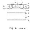
- a structure wherein the positive curvature parts 5a in FIG. 1 are completely enclosed i.e. the kind of structure illustrated in-FIG. 4, may be effective.
- Such a structure is well known to be effective for an APD composed of a single semiconductor, such as an Si-APD or a Ge-APD.
- the inventors tried to produce the structure of FIG. 4 by the use of compound semiconductors, and found it difficult to achieve uniform avalanche gain with a hiqh reproducibility, with its edge breakdown sufficiently restrained. Since the junction position of a guard ring 5' comes closer to the hetero-interface between an InGaAs layer 3 and an InP layer 4 than to a p +- n junction 5b as shown in FIG.
- the electric field strength in the InGaAs layer is greater in the region beneath the guard ring part than in the region beneath the p +- n junction part. Therefore, there emerges in the guard ring part an effect of the voltage breakdown in the InGaAs layer. This effect is the strongest in the positive curvature parts 5'a of the guard ring, and is due to the fact that voltage breakdown occurs in the positive curvature parts 5'a on the periphery of the guard ring before a breakdown takes place in the p +- n junction part.
- An object of the present invention is to obviate the aforementioned disadvantages and to provide a structure for a heterojunction APD capable of achieving sufficient and uniform avalanche gain in a stepwise p-n junction region corresponding to its light receiving region before a voltage breakdown occurs in its guard ring, and a method for the manufacture thereof.
- an avalanche photodiode comprises: a light absorbing semiconductor layer; an avalanche gain semiconductor layer having a bandgap greater than that of said light absorbing semiconductor layer; a first p-n junction having a substantially p +- n junction and selectively provided in said avalanche gain semiconductor layer; a second p-n junction having a substantially graded p-n junction surrounding the periphery of said first p-n junction; and a third p-n junction having a substantially graded p-n junction and surrounding the periphery of said second p-n junction.
- a specific feature of the invention is that said second p-n junction is positioned deeper from the upper surface than said first p-n junction and said third p-n junction is positioned closer to the upper surface than said second p-n junction.
- a composite guard ring structure wherein an inner first guard ring positioned close to the p +- n junction is so arranged as to be deeper than the p +-n junction, further the positive curvature of the periphery of the first guard ring is eased anew and, accordingly, a second guard ring, positioned shallower than the p-n junction of the first guard ring, is provided around the periphery of the first guard ring so as to ease the effect of voltage breakdown in the InGaAs layer thereof.
- This structure completely encloses the "positive curvature" in the depletion layer distribution in the peripheral part of the p -n junction and eases the positive curvature of the peripheral part of the guard rings, thereby contributing to the improvement of the breakdown voltage of the guard rings themselves.
- an avalanche photodiode comprises an n-InP buffer layer 2 (about 1 micron thick), an n -In 0.53 Ga 0.47 As layer 3 (about 3.5 microns thick) of 3 - 5 x 10 15 cm -3 in carrier concentration, lattice-matched to InP, an InGaAsP layer 3' (about 0.1 micron thick)having a band-gap corresponding to a wavelength of 1.3 microns, an n-InP layer 4 (1.5 to 2.5 microns thick) of 1-2 x 10 16 cm -3 in carrier concentration, and an n -InP layer 4' (1.5 to 2.0 microns thick) of 1 - 5 x 10 cm in carrier concentration, successively grown over a sulfur-doped (S-doped) n -InP substrate 1.
- S-doped sulfur-doped
- the n-InP buffer layer 2 is intended to prevent any defects or dislocations in the InP substrate 1 from reaching the layers 3 to 4' during the layer growth process; the n -InGaAs layer 3, to absorb light of 1 to 1.7 microns in wavelength and generating hole and electron carriers; the n-InGaAsP layer 3', to prevent transit delay of the hole carrier owing to discontinuity in the valence band maximum between the InP layer 4 and the InGaAs layer 3; the n-InP layer 4 is an avalanche gain layer; and the n -InP layer 4' is mainly intended to facilitate the expansion of a depletion layer in the peripheral part of the p-n junction, especially in its region close to the upper surface.
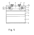
- the APD has a p type conductivity region (about 80 microns in diameter) selectively formed in the central part of the n-InP layer 4' in a round or an oval shape as viewed from above; a first guard ring 5'(about 100 microns in outer diameter) formed in the peripheral part of the p region in a ring form as viewed from above; and a second guard ring 5" (about 110 microns in outer diameter) formed in the peripheral part of the first guard ring 5 in a ring shape as viewed from the above.
- a p-electrode 7 is provided in a ring form over the p type conductivity region 5 through a window selectively bored into a surface passivation film 6, and an n-electrode is formed all over the lower surface of the substrate 1.
- the layers 2, 3, 3', 4 and 4' were grown over the InP substrate 1 etched with a mixture of H 2 SO 4 , H 2 O and H 2 0 2 in a ratio of 3:1:1, by hydride transport vapor phase epitaxy at a substrate temperature of 700°C in a reactor combining an InP ' growth chamber, an InGaAsP growth chamber and an InGaAs growth chamber.
- beryllium ion implantation was applied to realize the guard ring structure illustrated in FIG. 5. This method was used in view of the fact that a p-n junction resembling a graded type could be most readily formed with beryllium.
- SiO 2 film about 1 micron thick, was deposited at 370°C over the layer 4' by the pyrolytic chemical vapor deposition method (hereinafter abbreviated to the pyrolytic CVD method); the SiO 2 film was selectively removed in a ring pattern by a buffered fluoric acid etching solution with a photo-resist mask having a window of a ring pattern, and afterwards beryllium ions were implanted to provide the first guard ring 5' in an accelerating voltage range of 100 to 140 kV and in a dosage of 3 to 5 x 10 15 cm- 2 . In this process, beryllium ions were implanted only into the InP crystals exposed by the selective boring of the SiO 2 film.
- the pyrolytic chemical vapor deposition method hereinafter abbreviated to the pyrolytic CVD method
- the diameter of the ring-shaped window bored into the Si0 2 film was enlarged by common light-exposure and etching techniques, and beryllium ions were again implanted to form the second guard ring 5" in an accelerating voltage range of 70 to 100 kV and in a dosage of 1 to 3 x 10 13 cm- 2 .
- the lower the ion accelerating voltage (i.e. the shorter the projection range of ions) and the smaller the dose of implanted ions the lower the concentration of implanted ions at a given depth from the surface. This trend would remain unchanged even if, after ion implantation, thermal treatment for activation is conducted to form a conductivity region.
- the implantation accelerating voltage and the dosage were selected lower than those for the formation of the first guard ring so that the junction position of the second guard ring could be shallower from the surface than that of the first.
- the Si0 2 film was removed by etching with fluoric acid solution; then a phosphorous-silicate glass (PSG) film was deposited to a thickness of about 100 nm at 370°C by the pyrolytic CVD method, and thermal treatment at 700°C was performed for 20 minutes for the activation and drive-in diffusion of beryllium ions to form the first guard ring 5' and the second guard ring 5" to constitute graded p-n junctions.
- the p type conductivity region 5 was so formed by the thermal diffusion of cadmium that the stepwise p-n junction would be positioned about 0.5 micron shallower from the surface than the junction position of the first guard ring.
- the diffusion was done for 20 to 30 minutes at 570°C through the PSG film, with a round window selectively bored by the use of an exposure mask within the guard rings.
- the SiN surface passivation film 6 was deposited to a thickness of 150 to 200 nm by the plasma enhanced CVD method at 300°C, and after that, a window was selectively bored on the p type conductivity region 5 by the light exposure technique using a photo-resist mask on which a ring-shaped pattern was drawn, followed by the successive deposition of titanium, platinum and gold to thicknesses of 100 nm, 100 nm and 300 nm, respectively, by the electron-bombardment vaporization method to form the p-electrode 7. Further, the n-electrode was formed on the lower surface of the substrate 1 by the resistive heating vaporization method using AuGe/Ni alloy.
- the voltage at which the end of the depletion layer would reach the InGaAs layer when a reverse bias voltage was applied was about 30 V in the guard ring section, and about 40 V in the p +- n junction 5. Since the depletion layer reaches the InGaAs layer at a lower voltage in the guard ring section than in the p +- n junction, it is evident that the invention serves to obviate the "positive curvature" in the peripheral part of the p + -n junction, which was observed in the conventional depletion layer distribution shown in FIG. 3.
- the breakdown voltage of the completed APD ranged from 100 to 110 V, lower than the 120 to 150 V breakdown voltage of the guard ring section. Accordingly, the avalanche multiplication was sufficiently achieved in the p +- n junction corresponding to the light receiving region surrounded by the ring-shaped-electrode 7. This effect is illustrated in FIG. 6, wherein 11 represents a typical gain sensitivity distribution, well indicating a greater avalanche gain in the p +- n junction corresponding to the light receiving region than in the guard ring section.
- the maximum avalanche gain factor was from 40 to 60. In contrast to the maximum gain factor of less than 10 that could be previously achieved under the limitation of edge breakdown, the advantage of the present invention is evident.
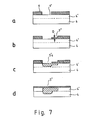
- FIGS. 7a to 7d are intended for describing a second preferred embodiment of the present invention, one of whose specific features is the method of forming its guard rings. What was said about the first embodiment holds exactly true with the structures of the semiconductor substrate and the epitaxial layers formed thereover for this APD and their manufacturing method.
- FIGS. 7a to 7d is illustrated only the right hand side of the bilaterally symmetrical section of an n-InP layer 4 and an n -InP layer 4' alone, which play a part in the formation of guard rings.
- the left contour line of each drawing corresponds to the central axis of the APD that is produced. Therefore, in the ensuring process, the left side simultaneously undergoes the same processing.
- an Si0 2 film was deposited over the n -InP layer 4' to a thickness of about 1 micron by the pyrolytic CVD method at 370°C, and a ring-shaped window region 9' was selectively bored to form a guard ring by the conventional exposure technique using an exposure mask on which a ring pattern was drawn (FIG. 7a).
- the ring measures 100 microns in inner diameter and 10 microns in width. Buffered fluoric acid solution was used for the etching removal of the SiO 2 film.
- the SiO 2 film on the the periphery of the ring-shaped window region 9' was thinned to form an approximately 10 micron wide ring 9" of about 100 nm in thickness by the use of buffered fluoric acid etching solution (FIG. 7b).
- This 100 nm thickness was selected for the purpose of making the ring thinner than the 300 to 500 nm projection range of beryllium ions to be implanted at the next step.
- the implantation mask 9 was fully removed with fluoric acid solution, and instead a PSG film for protection against thermal treatment was deposited all over the n -InP layer 4' to a thickness of about 100 nm by the pyrolytic CVD method at 370°C.
- thermal treatment was performed at 700°C for 20 minutes for the purpose of activation and drive-in diffusion of beryllium ions to form a guard ring 5', which would constitute an graded p-n junction (FIG. 7d).
- the shape of the guard ring thereby formed, as illustrated in FIG. 7d, was exactly identical with the envelope shape of the dual guard rings shown in FIG. 5.
- the punch-through voltage and breakdown voltage of the guard ring were checked up at this point of time, and found to be 30 to 40 V and 120 to 150 V, respectively. Then a p +- n junction, a surface passivation film and p- and n-electrodes were formed by exactly the same manufacturing methods as in the first preferred embodiment to complete an APD.
- the breakdown voltage of the APD completed was within the range of 100 to 110 V, lower than the 120 to 150 V breakdown voltage of the aforementioned guard ring.
- the punch-through voltage at the p +- n junction ranged from 40 to 50 V, about 10 V larger than the 30 to 40 V of the guard ring section. This means the absence of the "positive curvature" in the periphery of the step p +- n junction, which was present in the conventional depletion layer distribution as shown in FIG. 3.
- the distribution of avalanche gain sensitivity like in the first preferred embodiment, is such as illustrated in FIG. 6, with a maximum avalanche gain factor of 40 to 60 times.
- FIGS. 8a to 8d illustrate a third preferred embodiment of the photodetector manufacturing method according to the present invention, and in particular are intended for describing guard ring formation. Since the structures of the semiconductor substrate and the epitaxial layers formed thereover for this APD and their manufacturing method are exactly identical with those for the first embodiment, only an n-InP layer 4 and an n -InP layer 4', which play a part in guard ring formation, are illustrated here. In these figures again, only the right hand side of the bilaterally symmetrical section is shown. Therefore, in the ensuing process, the left side simultaneously undergoes the same processing as the right side.
- an SiO 2 film was deposited over the n -InP layer 4' to a thickness of about 1 micron by the pyrolytic CVD method at 370°C, and a ring-shaped window region 9' was selectively bored to form a guard ring by the conventional exposure technique using an photo-resist mask on which a ring pattern was drawn (FIG. 8a).
- the ring measures 100 microns in inner diameter and 10 microns in width. Buffered fluoric acid solution was used for the etching removal of the SiO 2 film.
- beryllium ions were implanted via the ion implantation mask 9 at an accelerating voltage of 100 to 140 kV and in a dosage of 3 to 5 x 10 13 cm -2 into n .-InP crystals exposed in the selectively opened region 9' to achieve a beryllium ion distribution 5'e (FIG. 8b). Then, an approximately 0.5 micron thickness of the InP layer on the periphery of the ring into which beryllium ions had been implanted was removed, in a 5 micron wide ring form, by etching with a mixture of H 2 SO 4 , H 2 0 and H 2 0 2 in a ratio of 3:1:1 to form a lower step 5'c (FIG. 8c).
- the number of beryllium ions present below the lower step 5'c is sufficiently smaller than the initially implanted number of 3 to 5 x 10 13 cm- 2 .
- thermal treatment for the activation and drive-in diffusion is performmed where there is a difference in implanted ion concentration beryllium is diffused more deeply in the high-concentration region than in the low-concentration region to form a p-type conductivity region 5' as illustrated in FIG. 8d.
- the implantation mask 9 was fully removed and instead a PSG film for protection against thermal treatment was deposited all over the n -InP layer 4' to a thickness of about 100 nm by the pyrolytic CVD method at 370°C, and then thermal treatment was performed at 700°C for 20 minutes to form a guard ring 5', which would constitute a graded p-n junction (FIG. 8d). Then a p +- n junction, a surface passivation film and p- and n-electrodes were formed by exactly the same manufacturing methods as in the first preferred embodiment to complete an APD.
Abstract
Description
- The present invention relates to a semiconductor photodetector, and more particularly to a pianar type heterojunction avalanche photodetector having a guard ring effect and its manufacturing method.
- Attempts are being made to develop avalanche photodiodes (APDs) using In0.53Ga0.47As as light detectors for use in optical communications in the 1.0 to 1.6 micron wavelength region, where the transmission loss of optical fibers is relatively small. Since In0.53Ga0.47As is lattice-matched to InP, and permits the formation of a heterojunction,it is possible to realize a photodetector which uses InGaAs and InP as a light absorbing layer and an avalanche gain layer, respectively. Such a photodetector is designed to achieve avalanche gain by conveying either the electron or the hole carrier which is generated in the InGaAs layer by optical excitation to the InP avalanche gain layer, resulting in reduction in dark current and excess noise and accordingly in a higher receiver sensitivity. K. Nishida et al. proposed this idea in Appl. Phys. Lett., Vol. 35, No. 3, pp. 251 - 253 (1979). FIG. 1 illustrates the structure proposed by Nishida et al., wherein a p+-n junction is formed by providing a p-
type conductivity region 5 after successively growing an n-InP buffer layer 2, an n--In0.53 Ga0.47Aslayer 3, an n-InP layer 4 and an n -InP layer 4'. The p+-n junction is sometimes called a one-sided abrupt or a one-sided step junction wherein acceptor impurity concentration is much greater than donor impurity concentration particularly out of abrupt or step p-n junctions. In the abrupt or step junction, the impurity concentration in a semiconductor changes abruptly from acceptor impurities to donor impurities. Therefore, when a reverse bias voltage is applied to the p-n junction, the conductivity region with lower carrier concentration is selectively depleted. Further in FIG. 1,reference numerals InGaAs layer 3, the InGaAs layer having a smaller bandgap absorbes light and only the positive hole carrier generated therein is conveyed to the p+-n junction formed in theInP layer 4 having a larger bandgap to achieve avalanche gain. A voltage breakdown occurs in theInP layer 4 with the generation of a tunnel current from theInGaAs layer 3 suppressed, achieving a low dark current photodetector. - In the structure of FIG. 1, however, the
peripheral part 5a of the selectively formed p+-n junction has its center of curvature within the p-type conductivity region 5 (this being referred to as having a "positive curvature") and, when a reverse bias voltage is applied to the p-n junction, high electric field concentrates in this "positive curvature"part 5a, resulting in a voltage breakdown thereat at a voltage lower than in theplanary part 5b of the p-n junction (a so-called edge breakdown). This edge breakdown is particularly conspicuous when the carrier concentration of theInGaAs layer 3 is much lower than that of theInP layer 4. This fact means that no sufficient carrier avalanche gain is achieved in theplanary part 5b corresponding to the light receiving region. - T. Shirai et al. proposed the structure illustrated in FIG. 2 to suppress this edge breakdown (Electron. Lett., Vol. 19, No. 14, pp. 534-535, 1983). In this structure, a p-type conductivity region 5' (a so-called guard ring), wherein a graded p-n junction whose breakdown voltage is higher than in a p+-n junction, or another p-n junction which can be approximated to the graded type is provided in such a position in the peripheral part of the p+-n junction that the depth from the surface of the graded or similar p-n junction is substantially equal to that of the p+-n junction. The graded p-n junction here means a p-n junction wherein concentrations of donor and acceptor change substantially linearly in the vicinity of the p-n junction. Accordingly, a junction whose depletion region, when a reverse bias voltage is applied to the graded p-n junction, is extended approximately equally toward the p-type and n-type conductivity regions. Even with the structure of FIG. 2, however, it is difficult to realize high avalanche gain while preventing the edge breakdown. The reason will be explained below. When a reverse bias voltage is applied to the p-n junction, while the depletion region of a p+-n junction grows mainly toward the n-type conductivity region, that in a graded p-n junction grows divided toward both the p-type and n-type conductivity regions. Therefore, the peripheral depletion region ends5a of a p+-n junction have positive curvatures, as indicated by the
depletion distribution 5d marked with oblique lines in FIG. 3 and accordingly, like in the aforementioned case of FIG. 1, an edge breakdown is apt to ultimately occur in this positive curvature part. - Then a structure wherein the
positive curvature parts 5a in FIG. 1 are completely enclosed, i.e. the kind of structure illustrated in-FIG. 4, may be effective. Such a structure is well known to be effective for an APD composed of a single semiconductor, such as an Si-APD or a Ge-APD. However, the inventors tried to produce the structure of FIG. 4 by the use of compound semiconductors, and found it difficult to achieve uniform avalanche gain with a hiqh reproducibility, with its edge breakdown sufficiently restrained. Since the junction position of a guard ring 5' comes closer to the hetero-interface between anInGaAs layer 3 and anInP layer 4 than to a p+-n junction 5b as shown in FIG. 4, the electric field strength in the InGaAs layer is greater in the region beneath the guard ring part than in the region beneath the p+-n junction part. Therefore, there emerges in the guard ring part an effect of the voltage breakdown in the InGaAs layer. This effect is the strongest in the positive curvature parts 5'a of the guard ring, and is due to the fact that voltage breakdown occurs in the positive curvature parts 5'a on the periphery of the guard ring before a breakdown takes place in the p+-n junction part. - An object of the present invention, therefore, is to obviate the aforementioned disadvantages and to provide a structure for a heterojunction APD capable of achieving sufficient and uniform avalanche gain in a stepwise p-n junction region corresponding to its light receiving region before a voltage breakdown occurs in its guard ring, and a method for the manufacture thereof.
- According to the invention, an avalanche photodiode comprises: a light absorbing semiconductor layer; an avalanche gain semiconductor layer having a bandgap greater than that of said light absorbing semiconductor layer; a first p-n junction having a substantially p+-n junction and selectively provided in said avalanche gain semiconductor layer; a second p-n junction having a substantially graded p-n junction surrounding the periphery of said first p-n junction; and a third p-n junction having a substantially graded p-n junction and surrounding the periphery of said second p-n junction.
- A specific feature of the invention is that said second p-n junction is positioned deeper from the upper surface than said first p-n junction and said third p-n junction is positioned closer to the upper surface than said second p-n junction.
- With accordance with the invention, there is used a composite guard ring structure wherein an inner first guard ring positioned close to the p+-n junction is so arranged as to be deeper than the p +-n junction, further the positive curvature of the periphery of the first guard ring is eased anew and, accordingly, a second guard ring, positioned shallower than the p-n junction of the first guard ring, is provided around the periphery of the first guard ring so as to ease the effect of voltage breakdown in the InGaAs layer thereof. This structure completely encloses the "positive curvature" in the depletion layer distribution in the peripheral part of the p -n junction and eases the positive curvature of the peripheral part of the guard rings, thereby contributing to the improvement of the breakdown voltage of the guard rings themselves.
-
- FIGS. 1, 2 and 4 are sectional views of prior art APD structures;
- FIG. 3 is a sectional view for describing the edge breakdown of the structure of FIG. 2;
- FIG. 5 is a sectional view of an APD which is one preferred embodiment of the present invention;
- FIG. 6 shows a gain sensitivity distribution profile of the APD according to the invention;
- FIGS. 7ato 7d are sectional views for describing a manufacturing method of the APD according to the invention; and
- FIGS. 8a to 8d are sectional views for describing another manufacturing method of the APD according to the invention.
- Although the following detailed description refers to a preferred embodiment using an InP/InGaAs-based hetero-junction APD, it may be readily understood that the principle of the invention can be applied exactly as effectively to other hetero-junctions, including AlGaAs/GaAs, AlGaAs/GaSb junctions and so on.
- Referring to FIG. 5, an avalanche photodiode (APD) comprises an n-InP buffer layer 2 (about 1 micron thick), an n -In0.53Ga0.47As layer 3 (about 3.5 microns thick) of 3 - 5 x 1015 cm-3 in carrier concentration, lattice-matched to InP, an InGaAsP layer 3' (about 0.1 micron thick)having a band-gap corresponding to a wavelength of 1.3 microns, an n-InP layer 4 (1.5 to 2.5 microns thick) of 1-2 x 1016 cm-3 in carrier concentration, and an n -InP layer 4' (1.5 to 2.0 microns thick) of 1 - 5 x 10 cm in carrier concentration, successively grown over a sulfur-doped (S-doped) n -
InP substrate 1. The n-InP buffer layer 2 is intended to prevent any defects or dislocations in theInP substrate 1 from reaching thelayers 3 to 4' during the layer growth process; the n -InGaAs layer 3, to absorb light of 1 to 1.7 microns in wavelength and generating hole and electron carriers; the n-InGaAsP layer 3', to prevent transit delay of the hole carrier owing to discontinuity in the valence band maximum between theInP layer 4 and theInGaAs layer 3; the n-InP layer 4 is an avalanche gain layer; and the n -InP layer 4' is mainly intended to facilitate the expansion of a depletion layer in the peripheral part of the p-n junction, especially in its region close to the upper surface. Further the APD has a p type conductivity region (about 80 microns in diameter) selectively formed in the central part of the n-InP layer 4' in a round or an oval shape as viewed from above; a first guard ring 5'(about 100 microns in outer diameter) formed in the peripheral part of the p region in a ring form as viewed from above; and asecond guard ring 5" (about 110 microns in outer diameter) formed in the peripheral part of thefirst guard ring 5 in a ring shape as viewed from the above. A p-electrode 7 is provided in a ring form over the ptype conductivity region 5 through a window selectively bored into asurface passivation film 6, and an n-electrode is formed all over the lower surface of thesubstrate 1. - The
layers InP substrate 1 etched with a mixture of H2SO4, H2O and H202 in a ratio of 3:1:1, by hydride transport vapor phase epitaxy at a substrate temperature of 700°C in a reactor combining an InP' growth chamber, an InGaAsP growth chamber and an InGaAs growth chamber. After the epitaxial laminated structure was formed, beryllium ion implantation was applied to realize the guard ring structure illustrated in FIG. 5. This method was used in view of the fact that a p-n junction resembling a graded type could be most readily formed with beryllium. An SiO2 film, about 1 micron thick, was deposited at 370°C over the layer 4' by the pyrolytic chemical vapor deposition method (hereinafter abbreviated to the pyrolytic CVD method); the SiO2 film was selectively removed in a ring pattern by a buffered fluoric acid etching solution with a photo-resist mask having a window of a ring pattern, and afterwards beryllium ions were implanted to provide the first guard ring 5' in an accelerating voltage range of 100 to 140 kV and in a dosage of 3 to 5 x 1015 cm-2. In this process, beryllium ions were implanted only into the InP crystals exposed by the selective boring of the SiO2 film. - Then, the diameter of the ring-shaped window bored into the Si02 film was enlarged by common light-exposure and etching techniques, and beryllium ions were again implanted to form the
second guard ring 5" in an accelerating voltage range of 70 to 100 kV and in a dosage of 1 to 3 x 1013 cm-2. Generally in ion implantation, the lower the ion accelerating voltage (i.e. the shorter the projection range of ions) and the smaller the dose of implanted ions, the lower the concentration of implanted ions at a given depth from the surface. This trend would remain unchanged even if, after ion implantation, thermal treatment for activation is conducted to form a conductivity region. Therefore, in implanting ions for the formation of the second guard ring, the implantation accelerating voltage and the dosage were selected lower than those for the formation of the first guard ring so that the junction position of the second guard ring could be shallower from the surface than that of the first. After implanting ions for the formation of the first and second guard rings, the Si02 film was removed by etching with fluoric acid solution; then a phosphorous-silicate glass (PSG) film was deposited to a thickness of about 100 nm at 370°C by the pyrolytic CVD method, and thermal treatment at 700°C was performed for 20 minutes for the activation and drive-in diffusion of beryllium ions to form the first guard ring 5' and thesecond guard ring 5" to constitute graded p-n junctions. After that, the ptype conductivity region 5 was so formed by the thermal diffusion of cadmium that the stepwise p-n junction would be positioned about 0.5 micron shallower from the surface than the junction position of the first guard ring. The diffusion was done for 20 to 30 minutes at 570°C through the PSG film, with a round window selectively bored by the use of an exposure mask within the guard rings. Then, after removing the PSG film with fluoric acid solution, the SiNsurface passivation film 6 was deposited to a thickness of 150 to 200 nm by the plasma enhanced CVD method at 300°C, and after that, a window was selectively bored on the ptype conductivity region 5 by the light exposure technique using a photo-resist mask on which a ring-shaped pattern was drawn, followed by the successive deposition of titanium, platinum and gold to thicknesses of 100 nm, 100 nm and 300 nm, respectively, by the electron-bombardment vaporization method to form the p-electrode 7. Further, the n-electrode was formed on the lower surface of thesubstrate 1 by the resistive heating vaporization method using AuGe/Ni alloy. - In order to check up the breakdown voltage of the guard rings, along with the foregoing process, there were also formed, by the use of wafers having the same epitaxial stratified structure, an graded p-n junction having only the first guard ring and another graded p-n junction of a structure in which the periphery of the first guard ring was surrounded by the second guard ring. The breakdown voltage of the p-n junction having the first guard ring alone was 100 to 120 V, while that of the other junction having two guard rings was 120 to 150 V, realizing the advantage of the present invention. Further the voltage at which the end of the depletion layer would reach the InGaAs layer when a reverse bias voltage was applied, namely the punch-through voltage, was about 30 V in the guard ring section, and about 40 V in the p+-n junction 5. Since the depletion layer reaches the InGaAs layer at a lower voltage in the guard ring section than in the p+-n junction, it is evident that the invention serves to obviate the "positive curvature" in the peripheral part of the p+-n junction, which was observed in the conventional depletion layer distribution shown in FIG. 3.
- The breakdown voltage of the completed APD ranged from 100 to 110 V, lower than the 120 to 150 V breakdown voltage of the guard ring section. Accordingly, the avalanche multiplication was sufficiently achieved in the p+-n junction corresponding to the light receiving region surrounded by the ring-shaped-
electrode 7. This effect is illustrated in FIG. 6, wherein 11 represents a typical gain sensitivity distribution, well indicating a greater avalanche gain in the p+-n junction corresponding to the light receiving region than in the guard ring section. The maximum avalanche gain factor was from 40 to 60. In contrast to the maximum gain factor of less than 10 that could be previously achieved under the limitation of edge breakdown, the advantage of the present invention is evident. - FIGS. 7a to 7d are intended for describing a second preferred embodiment of the present invention, one of whose specific features is the method of forming its guard rings. What was said about the first embodiment holds exactly true with the structures of the semiconductor substrate and the epitaxial layers formed thereover for this APD and their manufacturing method. In FIGS. 7a to 7d, is illustrated only the right hand side of the bilaterally symmetrical section of an n-
InP layer 4 and an n -InP layer 4' alone, which play a part in the formation of guard rings. The left contour line of each drawing corresponds to the central axis of the APD that is produced. Therefore, in the ensuring process, the left side simultaneously undergoes the same processing. - As an
ion implantation mask 9, an Si02 film was deposited over the n -InP layer 4' to a thickness of about 1 micron by the pyrolytic CVD method at 370°C, and a ring-shaped window region 9' was selectively bored to form a guard ring by the conventional exposure technique using an exposure mask on which a ring pattern was drawn (FIG. 7a). The ring measures 100 microns in inner diameter and 10 microns in width. Buffered fluoric acid solution was used for the etching removal of the SiO2 film. Then, the SiO 2 film on the the periphery of the ring-shaped window region 9' was thinned to form an approximately 10 micronwide ring 9" of about 100 nm in thickness by the use of buffered fluoric acid etching solution (FIG. 7b). This 100 nm thickness was selected for the purpose of making the ring thinner than the 300 to 500 nm projection range of beryllium ions to be implanted at the next step. Therefore, when beryllium ions were implanted at an accelerating voltage ranging from 100 to 140 kV and in a dosage of 3 to 5 x 1013 cm-2, the beryllium implanted through thethin film ring 9" was positioned lower and less concentrated than that implanted into the window region 9' as shown in FIG. 7c. - After that, the
implantation mask 9 was fully removed with fluoric acid solution, and instead a PSG film for protection against thermal treatment was deposited all over the n -InP layer 4' to a thickness of about 100 nm by the pyrolytic CVD method at 370°C. In this state, thermal treatment was performed at 700°C for 20 minutes for the purpose of activation and drive-in diffusion of beryllium ions to form a guard ring 5', which would constitute an graded p-n junction (FIG. 7d). The shape of the guard ring thereby formed, as illustrated in FIG. 7d, was exactly identical with the envelope shape of the dual guard rings shown in FIG. 5. The punch-through voltage and breakdown voltage of the guard ring were checked up at this point of time, and found to be 30 to 40 V and 120 to 150 V, respectively. Then a p+-n junction, a surface passivation film and p- and n-electrodes were formed by exactly the same manufacturing methods as in the first preferred embodiment to complete an APD. - The breakdown voltage of the APD completed was within the range of 100 to 110 V, lower than the 120 to 150 V breakdown voltage of the aforementioned guard ring. The punch-through voltage at the p+-n junction ranged from 40 to 50 V, about 10 V larger than the 30 to 40 V of the guard ring section. This means the absence of the "positive curvature" in the periphery of the step p+-n junction, which was present in the conventional depletion layer distribution as shown in FIG. 3. Further, the distribution of avalanche gain sensitivity, like in the first preferred embodiment, is such as illustrated in FIG. 6, with a maximum avalanche gain factor of 40 to 60 times.
- FIGS. 8a to 8d illustrate a third preferred embodiment of the photodetector manufacturing method according to the present invention, and in particular are intended for describing guard ring formation. Since the structures of the semiconductor substrate and the epitaxial layers formed thereover for this APD and their manufacturing method are exactly identical with those for the first embodiment, only an n-
InP layer 4 and an n -InP layer 4', which play a part in guard ring formation, are illustrated here. In these figures again, only the right hand side of the bilaterally symmetrical section is shown. Therefore, in the ensuing process, the left side simultaneously undergoes the same processing as the right side. - As an
ion implantation mask 9, an SiO2 film was deposited over the n -InP layer 4' to a thickness of about 1 micron by the pyrolytic CVD method at 370°C, and a ring-shaped window region 9' was selectively bored to form a guard ring by the conventional exposure technique using an photo-resist mask on which a ring pattern was drawn (FIG. 8a). The ring measures 100 microns in inner diameter and 10 microns in width. Buffered fluoric acid solution was used for the etching removal of the SiO2 film. Next, beryllium ions were implanted via theion implantation mask 9 at an accelerating voltage of 100 to 140 kV and in a dosage of 3 to 5 x 1013 cm-2 into n .-InP crystals exposed in the selectively opened region 9' to achieve a beryllium ion distribution 5'e (FIG. 8b). Then, an approximately 0.5 micron thickness of the InP layer on the periphery of the ring into which beryllium ions had been implanted was removed, in a 5 micron wide ring form, by etching with a mixture of H2SO4, H20 and H202 in a ratio of 3:1:1 to form a lower step 5'c (FIG. 8c). Accordingly, the number of beryllium ions present below the lower step 5'c is sufficiently smaller than the initially implanted number of 3 to 5 x 1013 cm-2. When thermal treatment for the activation and drive-in diffusion is performmed where there is a difference in implanted ion concentration beryllium is diffused more deeply in the high-concentration region than in the low-concentration region to form a p-type conductivity region 5' as illustrated in FIG. 8d. Thus, after the ion implantation, theimplantation mask 9 was fully removed and instead a PSG film for protection against thermal treatment was deposited all over the n -InP layer 4' to a thickness of about 100 nm by the pyrolytic CVD method at 370°C, and then thermal treatment was performed at 700°C for 20 minutes to form a guard ring 5', which would constitute a graded p-n junction (FIG. 8d). Then a p+-n junction, a surface passivation film and p- and n-electrodes were formed by exactly the same manufacturing methods as in the first preferred embodiment to complete an APD. - The punch-through voltage, breakdown voltage and avalanche gain sensitivity distribution of the APD thereby completed were found substantially the same as those of the first preferred embodiment, and accordingly demonstrated the advantage of the present invention.
Claims (5)
Applications Claiming Priority (8)
| Application Number | Priority Date | Filing Date | Title |
|---|---|---|---|
| JP59054907A JPH065785B2 (en) | 1984-03-22 | 1984-03-22 | Method for manufacturing semiconductor light receiving element |
| JP54907/84 | 1984-03-22 | ||
| JP54908/84 | 1984-03-22 | ||
| JP59054908A JPH06101578B2 (en) | 1984-03-22 | 1984-03-22 | Planar heterojunction avalanche photodiode |
| JP223230/84 | 1984-10-24 | ||
| JP59223226A JPS61101084A (en) | 1984-10-24 | 1984-10-24 | Manufacture of compound semiconductor light-receiving element |
| JP223226/84 | 1984-10-24 | ||
| JP59223230A JPH06105795B2 (en) | 1984-10-24 | 1984-10-24 | Method for manufacturing group III-V semiconductor light receiving element |
Publications (2)
| Publication Number | Publication Date |
|---|---|
| EP0159544A1 true EP0159544A1 (en) | 1985-10-30 |
| EP0159544B1 EP0159544B1 (en) | 1988-12-28 |
Family
ID=27463128
Family Applications (1)
| Application Number | Title | Priority Date | Filing Date |
|---|---|---|---|
| EP85103299A Expired EP0159544B1 (en) | 1984-03-22 | 1985-03-21 | Avalanche photodiode and its manufacturing method |
Country Status (4)
| Country | Link |
|---|---|
| US (1) | US4651187A (en) |
| EP (1) | EP0159544B1 (en) |
| CA (1) | CA1261450A (en) |
| DE (1) | DE3567128D1 (en) |
Cited By (5)
| Publication number | Priority date | Publication date | Assignee | Title |
|---|---|---|---|---|
| EP0311816A1 (en) * | 1987-10-15 | 1989-04-19 | BBC Brown Boveri AG | Semiconductor element and its manufacturing method |
| EP0350505A1 (en) * | 1988-01-06 | 1990-01-17 | University Of Southern California | Avalanche photodiode |
| EP0373752A2 (en) * | 1988-12-14 | 1990-06-20 | Kabushiki Kaisha Toshiba | Semiconductor light detector and method of manufacturing the same |
| DE3921028A1 (en) * | 1989-06-27 | 1991-01-10 | Siemens Ag | Avalanche photodiode with mesa structure - including guard ring preventing edge breakdown |
| WO1996003774A1 (en) * | 1994-07-27 | 1996-02-08 | Siemens Aktiengesellschaft | Semiconductor component with a high blocking capability edge termination |
Families Citing this family (24)
| Publication number | Priority date | Publication date | Assignee | Title |
|---|---|---|---|---|
| JPS5854685A (en) * | 1981-09-28 | 1983-03-31 | Kokusai Denshin Denwa Co Ltd <Kdd> | Avalanche photodiode and manufacture thereof |
| JPS61172381A (en) * | 1984-12-22 | 1986-08-04 | Fujitsu Ltd | Inp group compound semiconductor device |
| FR2581482B1 (en) * | 1985-05-03 | 1987-07-10 | Labo Electronique Physique | LOW LEAKAGE CURRENT PIN PHOTODIODE |
| DE3678338D1 (en) * | 1985-05-20 | 1991-05-02 | Nec Corp | PLANAR HETEROUE TRANSITION-AVALANCHE-PHOTODIODE. |
| EP0216572B1 (en) * | 1985-09-24 | 1995-04-05 | Kabushiki Kaisha Toshiba | Semiconductor photo-detector having a two-stepped impurity profile |
| JPS62259481A (en) * | 1986-04-15 | 1987-11-11 | Fujitsu Ltd | Semiconductor light receiving device |
| EP0304048B1 (en) * | 1987-08-19 | 1997-05-28 | Nec Corporation | A planar type heterostructure avalanche photodiode |
| US4876209A (en) * | 1988-01-06 | 1989-10-24 | U.S.C. | Method of making avalanche photodiode |
| US5179430A (en) * | 1988-05-24 | 1993-01-12 | Nec Corporation | Planar type heterojunction avalanche photodiode |
| JP2942285B2 (en) * | 1989-08-24 | 1999-08-30 | 三菱電機株式会社 | Semiconductor light receiving element |
| US5179431A (en) * | 1989-11-20 | 1993-01-12 | Fujitsu Limited | Semiconductor photodetection device |
| US5610416A (en) * | 1995-02-16 | 1997-03-11 | Hewlett-Packard Company | Avalanche photodiode with epitaxially regrown guard rings |
| US6066883A (en) * | 1998-03-16 | 2000-05-23 | Xerox Corporation | Guarding for a CMOS photosensor chip |
| US6359293B1 (en) * | 1999-08-17 | 2002-03-19 | Agere Systems Guardian Corp. | Integrated optoelectronic device with an avalanche photodetector and method of making the same using commercial CMOS processes |
| KR100366046B1 (en) * | 2000-06-29 | 2002-12-27 | 삼성전자 주식회사 | Method of manufacturing avalanche phoetodiode |
| KR20020034100A (en) * | 2002-01-21 | 2002-05-08 | 주흥로 | Avalanche photodiode |
| US6730979B2 (en) | 2002-09-12 | 2004-05-04 | The Boeing Company | Recessed p-type region cap layer avalanche photodiode |
| KR100634444B1 (en) * | 2004-12-20 | 2006-10-16 | 삼성전자주식회사 | Photo detecting devices and methods of forming the same |
| US20060169969A1 (en) * | 2005-02-02 | 2006-08-03 | Nanodynamics 88 | Bandgap cascade cold cathode |
| US8871557B2 (en) * | 2011-09-02 | 2014-10-28 | Electronics And Telecommunications Research Institute | Photomultiplier and manufacturing method thereof |
| JP5857774B2 (en) * | 2012-02-09 | 2016-02-10 | 三菱電機株式会社 | Semiconductor photo detector |
| JP2015141936A (en) * | 2014-01-27 | 2015-08-03 | 三菱電機株式会社 | Method of manufacturing semiconductor device |
| EP3206234B1 (en) | 2016-02-09 | 2023-08-09 | ams AG | Semiconductor element with a single photon avalanche diode and method for manufacturing such semiconductor element |
| KR102284627B1 (en) * | 2019-12-04 | 2021-08-02 | 주식회사 시지트로닉스 | Light receiving semiconductor device and manufacturing method thereof |
Citations (4)
| Publication number | Priority date | Publication date | Assignee | Title |
|---|---|---|---|---|
| US3391287A (en) * | 1965-07-30 | 1968-07-02 | Westinghouse Electric Corp | Guard junctions for p-nu junction semiconductor devices |
| EP0053513A2 (en) * | 1980-12-02 | 1982-06-09 | Fujitsu Limited | Avalanche photodiodes |
| EP0061551A2 (en) * | 1981-03-28 | 1982-10-06 | Kabushiki Kaisha Toshiba | Planar type semiconductor device with a high breakdown voltage |
| GB2134705A (en) * | 1983-01-28 | 1984-08-15 | Philips Electronic Associated | Semiconductor devices |
-
1985
- 1985-03-19 US US06/713,669 patent/US4651187A/en not_active Expired - Lifetime
- 1985-03-21 EP EP85103299A patent/EP0159544B1/en not_active Expired
- 1985-03-21 DE DE8585103299T patent/DE3567128D1/en not_active Expired
- 1985-03-21 CA CA000477076A patent/CA1261450A/en not_active Expired
Patent Citations (4)
| Publication number | Priority date | Publication date | Assignee | Title |
|---|---|---|---|---|
| US3391287A (en) * | 1965-07-30 | 1968-07-02 | Westinghouse Electric Corp | Guard junctions for p-nu junction semiconductor devices |
| EP0053513A2 (en) * | 1980-12-02 | 1982-06-09 | Fujitsu Limited | Avalanche photodiodes |
| EP0061551A2 (en) * | 1981-03-28 | 1982-10-06 | Kabushiki Kaisha Toshiba | Planar type semiconductor device with a high breakdown voltage |
| GB2134705A (en) * | 1983-01-28 | 1984-08-15 | Philips Electronic Associated | Semiconductor devices |
Non-Patent Citations (1)
| Title |
|---|
| ELECTRONICS LETTERS, vol. 19, no. 2, 20th January 1983, pages 61-62, London, GB; M. IKEDA et al.: "Planar InP/InGaAs-APD with a guardring formed by Cd diffusion through SiO2" * |
Cited By (10)
| Publication number | Priority date | Publication date | Assignee | Title |
|---|---|---|---|---|
| EP0311816A1 (en) * | 1987-10-15 | 1989-04-19 | BBC Brown Boveri AG | Semiconductor element and its manufacturing method |
| US5093693A (en) * | 1987-10-15 | 1992-03-03 | Bbc Brown Boveri Ag | Pn-junction with guard ring |
| EP0350505A1 (en) * | 1988-01-06 | 1990-01-17 | University Of Southern California | Avalanche photodiode |
| EP0350505A4 (en) * | 1988-01-06 | 1990-09-05 | University Of Southern California | Avalanche photodiode |
| EP0373752A2 (en) * | 1988-12-14 | 1990-06-20 | Kabushiki Kaisha Toshiba | Semiconductor light detector and method of manufacturing the same |
| EP0373752A3 (en) * | 1988-12-14 | 1990-08-16 | Kabushiki Kaisha Toshiba | Semiconductor light detector and method of manufacturing the same |
| US5144381A (en) * | 1988-12-14 | 1992-09-01 | Kabushiki Kaisha Toshiba | Semiconductor light detector utilizing an avalanche effect and having an improved guard ring structure |
| DE3921028A1 (en) * | 1989-06-27 | 1991-01-10 | Siemens Ag | Avalanche photodiode with mesa structure - including guard ring preventing edge breakdown |
| WO1996003774A1 (en) * | 1994-07-27 | 1996-02-08 | Siemens Aktiengesellschaft | Semiconductor component with a high blocking capability edge termination |
| US5712502A (en) * | 1994-07-27 | 1998-01-27 | Siemens Aktiengesellschaft | Semiconductor component having an edge termination means with high field blocking capability |
Also Published As
| Publication number | Publication date |
|---|---|
| US4651187A (en) | 1987-03-17 |
| CA1261450A (en) | 1989-09-26 |
| DE3567128D1 (en) | 1989-02-02 |
| EP0159544B1 (en) | 1988-12-28 |
Similar Documents
| Publication | Publication Date | Title |
|---|---|---|
| EP0159544B1 (en) | Avalanche photodiode and its manufacturing method | |
| EP0053513B1 (en) | Avalanche photodiodes | |
| US5157473A (en) | Avalanche photodiode having guard ring | |
| US7187013B2 (en) | Avalanche photodiode | |
| EP0043734B1 (en) | Avalanche photodiodes | |
| JP2762939B2 (en) | Superlattice avalanche photodiode | |
| US5843804A (en) | Method of making avalanche photodiodes with epitaxially-regrown guard rings | |
| JP3996699B2 (en) | Semiconductor photodetector | |
| EP0163295B1 (en) | A semiconductor photodetector and fabrication process for the same | |
| EP0163546B1 (en) | Process for fabricating an avalanche photodiode and an avalanche photodiode thus-obtained | |
| CA2007670C (en) | Semiconductor photodetector device and method of manufacturing the same | |
| EP0205899B1 (en) | Planar heterojunction avalanche photodiode | |
| EP0304048B1 (en) | A planar type heterostructure avalanche photodiode | |
| KR100509355B1 (en) | Photo-diode and method for fabricating the same | |
| JP3055030B2 (en) | Manufacturing method of avalanche photodiode | |
| JP2854634B2 (en) | Light receiving device | |
| JPH02253666A (en) | Semiconductor photodetector | |
| JPS61265876A (en) | Planar type hetero junction semiconductor photodetector | |
| JPS58170073A (en) | Semiconductor device | |
| JPS60173880A (en) | Semiconductor photodetector and manufacture thereof | |
| JPS61267375A (en) | Planar type hetero junction semiconductor photodetector | |
| JPH03296281A (en) | Manufacture of semiconductor photodetector | |
| JPH065786B2 (en) | Semiconductor device | |
| JPS60260167A (en) | Semiconductor light-receiving device |
Legal Events
| Date | Code | Title | Description |
|---|---|---|---|
| PUAI | Public reference made under article 153(3) epc to a published international application that has entered the european phase |
Free format text: ORIGINAL CODE: 0009012 |
|
| 17P | Request for examination filed |
Effective date: 19850321 |
|
| AK | Designated contracting states |
Designated state(s): DE FR GB NL |
|
| 17Q | First examination report despatched |
Effective date: 19870518 |
|
| GRAA | (expected) grant |
Free format text: ORIGINAL CODE: 0009210 |
|
| AK | Designated contracting states |
Kind code of ref document: B1 Designated state(s): DE FR GB NL |
|
| REF | Corresponds to: |
Ref document number: 3567128 Country of ref document: DE Date of ref document: 19890202 |
|
| ET | Fr: translation filed | ||
| PLBI | Opposition filed |
Free format text: ORIGINAL CODE: 0009260 |
|
| 26 | Opposition filed |
Opponent name: BRITISH TELECOMMUNICATIONS PUBLIC LIMITED COMPANY Effective date: 19890927 |
|
| NLR1 | Nl: opposition has been filed with the epo |
Opponent name: BRITISH TELECOMMUNICATIONS PUBLIC LIMITED COMPANY |
|
| PLBN | Opposition rejected |
Free format text: ORIGINAL CODE: 0009273 |
|
| STAA | Information on the status of an ep patent application or granted ep patent |
Free format text: STATUS: OPPOSITION REJECTED |
|
| 27O | Opposition rejected |
Effective date: 19911211 |
|
| NLR2 | Nl: decision of opposition | ||
| REG | Reference to a national code |
Ref country code: GB Ref legal event code: IF02 |
|
| PGFP | Annual fee paid to national office [announced via postgrant information from national office to epo] |
Ref country code: FR Payment date: 20040309 Year of fee payment: 20 |
|
| PGFP | Annual fee paid to national office [announced via postgrant information from national office to epo] |
Ref country code: NL Payment date: 20040310 Year of fee payment: 20 |
|
| PGFP | Annual fee paid to national office [announced via postgrant information from national office to epo] |
Ref country code: GB Payment date: 20040317 Year of fee payment: 20 |
|
| PGFP | Annual fee paid to national office [announced via postgrant information from national office to epo] |
Ref country code: DE Payment date: 20040401 Year of fee payment: 20 |
|
| PG25 | Lapsed in a contracting state [announced via postgrant information from national office to epo] |
Ref country code: GB Free format text: LAPSE BECAUSE OF EXPIRATION OF PROTECTION Effective date: 20050320 |
|
| PG25 | Lapsed in a contracting state [announced via postgrant information from national office to epo] |
Ref country code: NL Free format text: LAPSE BECAUSE OF EXPIRATION OF PROTECTION Effective date: 20050321 |
|
| REG | Reference to a national code |
Ref country code: GB Ref legal event code: PE20 |
|
| NLV7 | Nl: ceased due to reaching the maximum lifetime of a patent |
Effective date: 20050321 |