EP0155178A2 - Film de revêtement, procédé et appareil pour produire ce film - Google Patents
Film de revêtement, procédé et appareil pour produire ce film Download PDFInfo
- Publication number
- EP0155178A2 EP0155178A2 EP85301709A EP85301709A EP0155178A2 EP 0155178 A2 EP0155178 A2 EP 0155178A2 EP 85301709 A EP85301709 A EP 85301709A EP 85301709 A EP85301709 A EP 85301709A EP 0155178 A2 EP0155178 A2 EP 0155178A2
- Authority
- EP
- European Patent Office
- Prior art keywords
- substrate
- electrode
- plasma
- anode
- coating film
- Prior art date
- Legal status (The legal status is an assumption and is not a legal conclusion. Google has not performed a legal analysis and makes no representation as to the accuracy of the status listed.)
- Granted
Links
Images


Classifications
-
- H—ELECTRICITY
- H01—ELECTRIC ELEMENTS
- H01J—ELECTRIC DISCHARGE TUBES OR DISCHARGE LAMPS
- H01J37/00—Discharge tubes with provision for introducing objects or material to be exposed to the discharge, e.g. for the purpose of examination or processing thereof
- H01J37/32—Gas-filled discharge tubes
- H01J37/34—Gas-filled discharge tubes operating with cathodic sputtering
- H01J37/3402—Gas-filled discharge tubes operating with cathodic sputtering using supplementary magnetic fields
-
- C—CHEMISTRY; METALLURGY
- C23—COATING METALLIC MATERIAL; COATING MATERIAL WITH METALLIC MATERIAL; CHEMICAL SURFACE TREATMENT; DIFFUSION TREATMENT OF METALLIC MATERIAL; COATING BY VACUUM EVAPORATION, BY SPUTTERING, BY ION IMPLANTATION OR BY CHEMICAL VAPOUR DEPOSITION, IN GENERAL; INHIBITING CORROSION OF METALLIC MATERIAL OR INCRUSTATION IN GENERAL
- C23C—COATING METALLIC MATERIAL; COATING MATERIAL WITH METALLIC MATERIAL; SURFACE TREATMENT OF METALLIC MATERIAL BY DIFFUSION INTO THE SURFACE, BY CHEMICAL CONVERSION OR SUBSTITUTION; COATING BY VACUUM EVAPORATION, BY SPUTTERING, BY ION IMPLANTATION OR BY CHEMICAL VAPOUR DEPOSITION, IN GENERAL
- C23C14/00—Coating by vacuum evaporation, by sputtering or by ion implantation of the coating forming material
- C23C14/06—Coating by vacuum evaporation, by sputtering or by ion implantation of the coating forming material characterised by the coating material
- C23C14/0605—Carbon
-
- Y—GENERAL TAGGING OF NEW TECHNOLOGICAL DEVELOPMENTS; GENERAL TAGGING OF CROSS-SECTIONAL TECHNOLOGIES SPANNING OVER SEVERAL SECTIONS OF THE IPC; TECHNICAL SUBJECTS COVERED BY FORMER USPC CROSS-REFERENCE ART COLLECTIONS [XRACs] AND DIGESTS
- Y10—TECHNICAL SUBJECTS COVERED BY FORMER USPC
- Y10T—TECHNICAL SUBJECTS COVERED BY FORMER US CLASSIFICATION
- Y10T428/00—Stock material or miscellaneous articles
- Y10T428/30—Self-sustaining carbon mass or layer with impregnant or other layer
Definitions
- the present invention relates to a coating film of amorphous carbon and a method and apparatus for producing the same.
- a coating film of amorphous carbon generally has a high hardness, high oxidation resistance, high thermal resistance, high electrical resistance and high thermal conductivity.
- plastics materials and common metals are susceptible to surface scratch so that their surfaces, while initially having excellent luster, gradually lose their luster which damages their appearance. This has been considered to be due to the fact that these plastics material and metals are relatively soft and have low abrasion resistance.
- the cell In the case of a solar cell comprising amorphous silicon, etc., which contains a large amount of hydrogen or a large amount of hydrogen and fluorine, the cell essentially has a low energy converting efficiency and this is compensated for by means of an increased surface area or the like.
- a need for the development of materials of higher efficiencies for the surface coating films in view of the necessity to ensure a sufficient amount of incident light to the solar cell.
- the conventional silicon semiconductors are subject to the limitation that the forbidden band gap may be as narrow as 1.21 eV and they cannot be used at high temperatures, thus giving rise to a need for the development of a material having wider range of working temperatures.
- the conventional sputtering methods include one in which an argon plasma is produced by applying a voltage across an anode and a cathode in argon gas at a pressure of about 0.133 to 1.33 Pa (10 to 10 -2 Torr) and a target material is sputtered by the argon ion thereby forming an alloy coating on the substrate.
- a method of producing a coating film on a substrate which comprises sputtering a carbonaceous e.g. graphite target electrode in a vacuum chamber characterised in that the chamber contains hydrogen and/or fluorine gas at a pressure of between 6.665 and 666.5 Pa (0.05 and 5.0 Torr) while the temperature of the substrate is maintained between room temperature and 100°C and while maintaining the current density between the target electrode, and an anode at a value between 11.3 and 14.7 mA/cm 2 thereby producing an amorphous carbon coating film in which the value of H/C or (H + F)/C in terms of an atomic ratio is between 0.5 and 0.9, the current density being defined as the current through the anode per unit area of the target electrode.
- a carbonaceous e.g. graphite target electrode in a vacuum chamber characterised in that the chamber contains hydrogen and/or fluorine gas at a pressure of between 6.665 and 666.5 Pa (0.05 and 5.0 Torr) while the temperature of the substrate is
- an amorphous carbon coating film on a substrate characterised in that it is produced by sputtering a carbonaceous, e.g. graphite target electrode in an atmosphere of hydrogen and/or fluorine gas having a pressure of 6.665 to 666.5 Pa (0.05 to 5.0 Torr) while maintaining the temperature of the deposition substrate between room temperature and 100°C and while maintaining the current density between the target electrode and an anode at a value between 11.3 and 14.7 mA/cm 2 whereby the value of H/C or (H + F)/C in terms of an atomic ratio is between 0.5 and 0.9, the current density being defined as the current through the anode per unit area of the target electrode.
- a carbonaceous, e.g. graphite target electrode in an atmosphere of hydrogen and/or fluorine gas having a pressure of 6.665 to 666.5 Pa (0.05 to 5.0 Torr) while maintaining the temperature of the deposition substrate between room temperature and 100°C and while maintaining the current density between the target electrode and an an
- a sputtering apparatus for producing an amorphous carbon coating film on a substrate
- the apparatus comprising a vacuum chamber having an atmosphere gas inlet pipe, an exhaust pipe, an electron drawing anode, a carbonaceous, e.g. graphite target electrode connected to a power source and positioned opposite to the anode, and means for producing a magnetic field to provide a directionality for a plasma, characterised in that the substrate is arranged on an inner wall of the vacuum chamber in a region which is not directly exposed to the plasma.
- a sputtering apparatus for producing an amorphous carbon coating film on a substrate, the apparatus comprising a vacuum chamber having an atmosphere gas inlet pipe, an exhaust pipe, an electron drawing anode, a carbonaceous target electrode connected to a power source and positioned opposite to the anode, and means for producing a magnetic field to provide a directionality for a plasma, characterised by a further electrode arranged between the anode and the target electrode, the further electrode having a large number of holes for adjusting the amount of the plasma.
- the invention also extends to a method of producing a coating film comprising the steps of: selecting a gas from the group consisting of hydrogen, fluorine and a mixture of hydrogen and fluorine and maintaining a pressure of said gas within a vacuum chamber between 6.665 and 666.5 Pa (0.05 and 5.0 Torr); and sputtering a graphite target electrode in said vacuum chamber while maintaining a temperature of a deposition substrate between a room temperature and 100°C and a relative current density which is a ratio of a plate current value to an area of target electrode for said graphite target electrode and an anode between 11.3 and 14.7 mA/cm 2 thereby producing an amorphous carbon coating film in which the value of H/C or (H + F)/C in terms of an atomic ratio is between 0.5 and 0.9.
- the invention also extends to a coating deposited by such a method.
- the present invention has arisen from various studies and investigations made in view of the foregoing disadvantages of the conventional methods, in order to provide an amorphous carbon coating film having a high hardness, high oxidation resistance, high abrasion resistance, high thermal resistance, high thermal conductivity and high electric resistance properties. It has resulted in a production method and an apparatus capable of preventing for example various difficulties assumed to be due to the fact that a substrate is placed in a plasma and the production of a coating film of a material having excellent uniformity. This has led to the resulting discovery that an amorphous carbon coating film can be formed having excellent properties by effecting a sputtering operation including various specific parameters over and above a conventional sputtering method.
- the value of the H/C ratio can be reduced by effecting the sputtering operation with an increased gas pressure, that decreasing the H/C ratio of the coating material to 0.5 or less has the effect of reducing the hardness of the coating film thereby making it impractical, and that increasing the H/C ratio to exceed 0.9 is not desirable since the optical band gap or the electric resistance is decreased and hence the insulating capability is deteriorated.
- the range of working relative current densities should preferably be selected to be 11.3 to 14.7 mA/cm .
- a coating film of material produced in accordance with the present invention has a very high hardness, high thermal resistance and high electric resistance, is high in infrared ray transparency and is excellent in chemical resistance, moisture resistance and scratch resistance as will be seen from examples which will be described later. More specifically, the coating may enjoy thefollow- ing effects.
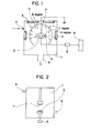
- numeral 1 designates a vacuum chamber, 4 an atmosphere gas inlet pipe, and 5 an exhaust pipe connected directly to a vacuum pump which is not shown to maintain a vacuum.
- Numeral 7 designates an electron drawing counter electrode at the ground potential, and 2 a carbonaceous electrode connected to a high frequency (RF) power source 6 through a matching box 8.
- RF radio frequency
- Numeral 3 designates deposition substrates arranged inside the container but outside the transport area of a plasma-excited source in contrast to conventional techniques. It is to be noted that hydrogen gas or any other gas is introduced the atmosphere gas inlet pipe 4.
- the interior of the vacuum chamber is considered divided into three regions, i. e . A region, B region and C region as schematically shown in the Figure 1.
- the A region represents the area enclosed by curved lines a which is the plasma state environment produced between the electrodes and the vicinity around the electrodes; carbon and hydrocarbon radicals consisting two carbon atoms or less such as C, CH, CH 2 , CH 3 , CH 4 , C 2 H 4 and C 2 H 6 are generated from the target electrode 2 in this region.
- the B region represents the area enclosed by a curved line b outside the electrodes 2 and 7 and in this region the above-mentioned particles contained in the plasma are transported at a velocity which is determined by the pressure of the atmosphere gas and the voltage across the electrodes.
- the C region represents the area other than the A region and the B region and in this region the transported particles are softly deposited on the deposition substrates arranged on the container inner walls.
- charged particles (constituting the majority of the transported particles) are susceptible to the effects of an electric field or the like, therefore it is necessary to take this into consideration so that the C region is maintained at a uniform potential, e.g., around ground potential.
- the substrates are never directly exposed to the plasma produced between the target electrode and the counter electrode so that the deposition and bombardment by protonsand electrons do not occur simultaneously at the substrate.
- a graphite target 2 of 75 mm ⁇ was placed inside a vacuum chamber 1 of a planer magnetron type sputtering apparatus shown by the schematic sectional view of Fig. 2 and a substrate material 3 consisting of an organic film, Si, glass, Al 2 O 3 or TiO 2 was mounted on a counter electrode 7 held at a distance of 45mm from the counter electrode 7.
- a vacuum was first produced within the vacuum chamber 1 by exhausting it to 1.333 x 10 -5 Pa (1 x 10 -7 Torr) by an exhauster which was not shown through an exhaust pipe 5 and then a hydrogen gas of 99.999 vol. % was introduced through an atmosphere gas inlet pipe 4 thereby holding the internal pressure of the chamber at 6.665 Pa (0.05 Torr).
- a high frequency power of 13.56 MHz was supplied from a power source 6 having a supply anode voltage of 2.3 kV and the sputtering was effected for two hours with a plate current of 0.5A (a relative current density was 11.3 mA/cm 2 ).
- the substrate temperature was controlled by water cooling to prevent it from exceeding 100°C.
- a lemon yellowish transparent thin film having a thickness of about 1 ⁇ m was formed on the substrate and the results of the observation by a scanning microscope having a resolving power of 6nm (60R) showed that the surface was quite smooth.
- the film was subjected to an elementary analysis showing that it contained carbon, hydrogen and nitrogen and its H/C atomic ratio was 0.90.
- electron diffraction and X-ray diffraction it was found that the film had no definite structure and thus it was an amorphous film.
- the optical band gap calculated from the visible ray absorption spectrum was 2.5 eV. Also, the film showed an electrical resistivity of 1 x 10 8 ⁇ cm which was close to that of insulators and a spin density of 5 x 10¹⁸ 1/cm 3 due to the electron spin resonance (ESR) and its hardness measured by a Vickers microhardness meter was 2,000.
- ESR electron spin resonance
- the electrical resistivity was 1 x 10 10 ⁇ cm, the spin density due to the ESR was 1 ⁇ 10 18 1/cm 3 and the hardness was 1,700.
- Example 1 was repeated except that a graphite target having attached thereonto a poly-4-ethylene fluoride sheet of an area corresponding to one half the target surface was used and that the hydrogen gas pressure was 66.65 Pa (0.5 Torr) and the supply voltage was 2.0kV.
- the resulting film had a thickness of 2 ⁇ m and an (H + F) / C atomic ratio of 0.8 and only the absorption due to C - H and C-F was observed by the IR absorption spectrum.
- the optical band gap was 2.8 eV
- the electric resistivity was 7 x 10 11 ⁇ cm and these properties were not deteriorated even in the air at 400°C.
- Example 1 was repeated except that the gas pressure in the vacuum chamber was held at 66.65 Pa (0.5 Torr) by means of a hydrogen gas of 99.999 vol. % and a fluorine gas of 99.999 vol. % and the supply voltage was 2.0 kV.
- the film showed a band gap of 3.1 eV and an electrical resistivity of 1 x 10 14 ⁇ cm and its spin density due to the ESR was 1 x 10 16 1/cm 3 . These properties were not changed even in the air at 400°C.
- Example 1 was repeated except that a dc voltage of 400 V was applied in place of the high frequency power.
- a lemon yellowish transparent film having a smooth surface and a thickness of 1 ⁇ m was formed on the substrate and its H/C atomic ratio was 0.9.
- the film was an amorphous carbon film containing diamond structures of 3nm or less in particle size in very small portions.
- Example 15 was performed in a condition where a dc bias voltage of 100 V was applied to the substrate.
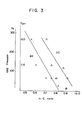
- Fig. 3 shows the relation between the H/C ratio and the gas pressure in the vacuum chamber for the amorphous films produced by Examples 1 to 16 and Fig. 4 shows the relation between the working current and the hardness for the amorphous films produced by Examples 1 to 5. From the behaviors shown in Fig. 3 it is apparent that increasing the atmosphere gas pressure during the sputtering operation decreases the H/C ratio of the resulting coating.
- the films were annealed in a vacuum or in argon for 1 hour at 400°C and no change was seen in their optical band gaps.
- sputtering was effected by a sputtering apparatus of the type shown in Fig. 5.
- a sputtering apparatus of the type shown in Fig. 5.
- the same reference numerals as used in Fig. 1 represent the same or equivalent components.
- the vacuum chamber 1 is composed of two covers and a cylinder having three flanges which are sealed with 0-rings.
- Numeral 10 designates a metal upper cover sealed with an O-ring.
- Numeral 12 designates a lower cover sealed by a sealing method which allows it to perform the same function as the upper cover 10. It is constructed so that a hermetic sealing can be provided by means of welding or the like, ignoring a specially provided opening 5.
- Numeral 13 designates insulating terminals or supports, 14 electrically grounded receptors, 3 deposition substrates made of an insulating material or metal, and 15 substrate supporting members.
- the deposition substrates 3 are arranged in positions on the upper and side walls of the chamber which are external to the plasma generating section and the travel path of the plasma, they are not neccessarily limited to these positions since it is only necessary that they are located outside the plasma excited source which is indicated as the C region in Fig. 1.
- Numeral 2 designates a carbonaceous target, 16 an electrode box, 17 a magnetron, 18 a cooling water supplying metal 'pipe, and 19 a drain pipe. The end of the cooling water pipe 18 outside the vacuum chamber is sealed watertight by welding.
- Numeral 20 designates a thermocouple.
- Numeral 7 designates a counter electrode for the target 2 and the target electrode 2 includes a connector which is provided outside the vacuum chamber 1 for connection with a high frequency power source.
- the matching box and the high frequency power source 6 shown in Fig. 1 are connected to the connector, although they are not shown.
- Numeral 4 designates an atmosphere gas inlet pipe connected to the vacuum chamber 1 so as to introduce an atmosphere gas consisting of hydrogen or hydrogen and fluorine.
- An exhaust pipe 5 is arranged to reduce the internal pressure of the vacuum chamber 1 through a vacuum pump which is not shown.
- the following table shows the results of a sputtering operation effected for 2 hours by applying a high frequency power of 13.56 MHz and using high-purity hydrogen of 99.999 vol. % as the atmosphere gas in a sputtering apparatus employing the above-mentioned deposition substrate arrangement and a sputtering apparatus having the substrate arranged in the same counter electrode position as previously for purposes of comparison.
- the sputtering conditions were as follows.
- the mesh electrode may literally be in the form of a mesh, it may also be a metal sheet formed with an innumerable number of pin holes so as to obtain the same effect as the mesh. Also, since the essential point is the adjustment of the amount of plasma, the invention is not limited to the method employing a grounded mesh and the same object can be accomplished by for example applying the potential supplied from a separate power supply to the plasma adjusting electrode.
- the amount of plasma may be adjusted by for example sliding the mesh to change its position as shown by the arrows in Fig. 6.
- Example 20 was repeated except that a fluorine gas or a mixed gas of hydrogen and fluorine was used in place of the hydrogen gas.
- the thermal resistance (the temperature at which the optical gap starts decreasing) attained by the amorphous carbon film was improved by the use of the mixed gas to from 300°C to 500°C.
- the use of carbon fluoride for the target improved the thermal resistance to 500°C.
Applications Claiming Priority (6)
| Application Number | Priority Date | Filing Date | Title |
|---|---|---|---|
| JP59046397A JPS60190557A (ja) | 1984-03-13 | 1984-03-13 | コ−テイング材およびその製法 |
| JP46397/84 | 1984-03-13 | ||
| JP16379684A JPS6142124A (ja) | 1984-08-06 | 1984-08-06 | スパツタ装置 |
| JP163795/84 | 1984-08-06 | ||
| JP163796/84 | 1984-08-06 | ||
| JP16379584A JPS6142123A (ja) | 1984-08-06 | 1984-08-06 | スパツタ装置 |
Publications (3)
| Publication Number | Publication Date |
|---|---|
| EP0155178A2 true EP0155178A2 (fr) | 1985-09-18 |
| EP0155178A3 EP0155178A3 (en) | 1987-04-01 |
| EP0155178B1 EP0155178B1 (fr) | 1992-08-12 |
Family
ID=27292595
Family Applications (1)
| Application Number | Title | Priority Date | Filing Date |
|---|---|---|---|
| EP85301709A Expired - Lifetime EP0155178B1 (fr) | 1984-03-13 | 1985-03-13 | Film de revêtement, procédé et appareil pour produire ce film |
Country Status (4)
| Country | Link |
|---|---|
| US (1) | US4597844A (fr) |
| EP (1) | EP0155178B1 (fr) |
| CA (1) | CA1232228A (fr) |
| DE (1) | DE3586465T2 (fr) |
Cited By (7)
| Publication number | Priority date | Publication date | Assignee | Title |
|---|---|---|---|---|
| EP0238085A2 (fr) * | 1986-03-20 | 1987-09-23 | The Perkin-Elmer Corporation | Couches de i-carbone et leur procédé de fabrication |
| EP0244874A2 (fr) * | 1986-05-08 | 1987-11-11 | Kabushiki Kaisha Meidensha | Matériau luminescent, son procédé de production, et élément semi-conducteur luminescent en faisant usage |
| EP0304201A1 (fr) * | 1987-08-19 | 1989-02-22 | The Regents Of The University Of California | Procédé de production de films composites à base de diamant, de diamant dopé et de diamant-nitrure de bore cubique |
| DE3821614A1 (de) * | 1988-06-27 | 1989-12-28 | Licentia Gmbh | Deckschicht aus amorphem kohlenstoff auf einem substrat, verfahren zur herstellung der deckschicht und verwendung der deckschicht |
| EP0231894B1 (fr) * | 1986-01-31 | 1991-12-11 | Kabushiki Kaisha Meidensha | Procédé de production d'un film à base de carbone |
| US5110679A (en) * | 1990-04-24 | 1992-05-05 | The Regents Of The University Of California | Hard carbon nitride and method for preparing same |
| CN102102171A (zh) * | 2011-01-28 | 2011-06-22 | 南通扬子碳素股份有限公司 | 表面沉积非晶碳薄膜降低石墨电极消耗的方法 |
Families Citing this family (66)
| Publication number | Priority date | Publication date | Assignee | Title |
|---|---|---|---|---|
| US4770940A (en) * | 1984-09-10 | 1988-09-13 | Ovonic Synthetic Materials Company | Glow discharge method of applying a carbon coating onto a substrate and coating applied thereby |
| DE3609503A1 (de) * | 1985-03-22 | 1986-10-02 | Canon K.K., Tokio/Tokyo | Heizwiderstandselement und heizwiderstand unter verwendung desselben |
| DE3609456A1 (de) * | 1985-03-23 | 1986-10-02 | Canon K.K., Tokio/Tokyo | Waermeerzeugender widerstand und waermeerzeugendes widerstandselement unter benutzung desselben |
| DE3609691A1 (de) * | 1985-03-23 | 1986-10-02 | Canon K.K., Tokio/Tokyo | Thermischer schreibkopf |
| US4845513A (en) * | 1985-03-23 | 1989-07-04 | Canon Kabushiki Kaisha | Thermal recording head |
| GB2175252B (en) * | 1985-03-25 | 1990-09-19 | Canon Kk | Thermal recording head |
| GB2176443B (en) * | 1985-06-10 | 1990-11-14 | Canon Kk | Liquid jet recording head and recording system incorporating the same |
| EP0221531A3 (fr) * | 1985-11-06 | 1992-02-19 | Kanegafuchi Kagaku Kogyo Kabushiki Kaisha | Substrat isolé bon conducteur de chaleur et procédé pour sa fabrication |
| JPH0676666B2 (ja) * | 1987-02-10 | 1994-09-28 | 株式会社半導体エネルギ−研究所 | 炭素膜作製方法 |
| CN1020477C (zh) * | 1987-08-10 | 1993-05-05 | 株式会社半导体能源研究所 | 含卤素的碳材料淀积方法 |
| US5190824A (en) * | 1988-03-07 | 1993-03-02 | Semiconductor Energy Laboratory Co., Ltd. | Electrostatic-erasing abrasion-proof coating |
| US6224952B1 (en) * | 1988-03-07 | 2001-05-01 | Semiconductor Energy Laboratory Co., Ltd. | Electrostatic-erasing abrasion-proof coating and method for forming the same |
| US5202156A (en) * | 1988-08-16 | 1993-04-13 | Canon Kabushiki Kaisha | Method of making an optical element mold with a hard carbon film |
| US5030494A (en) * | 1989-01-26 | 1991-07-09 | International Business Machines Corporation | Carbon overcoat for a thin film magnetic recording disk containing discrete clusters of tungsten (W) or tungsten carbide (WC) which project from the surface of the overcoat |
| JP2799875B2 (ja) * | 1989-05-20 | 1998-09-21 | 株式会社リコー | 液晶表示装置 |
| US5527596A (en) * | 1990-09-27 | 1996-06-18 | Diamonex, Incorporated | Abrasion wear resistant coated substrate product |
| US5637353A (en) * | 1990-09-27 | 1997-06-10 | Monsanto Company | Abrasion wear resistant coated substrate product |
| US5135808A (en) * | 1990-09-27 | 1992-08-04 | Diamonex, Incorporated | Abrasion wear resistant coated substrate product |
| GB2252333B (en) * | 1991-01-29 | 1995-07-19 | Spectra Physics Scanning Syst | Improved scanner window |
| JP2929779B2 (ja) * | 1991-02-15 | 1999-08-03 | トヨタ自動車株式会社 | 炭素被膜付撥水ガラス |
| WO1992016671A1 (fr) * | 1991-03-20 | 1992-10-01 | Canon Kabushiki Kaisha | Procede et dispositif de formation d'une couche mince par pulverisation |
| JPH07109034B2 (ja) * | 1991-04-08 | 1995-11-22 | ワイケイケイ株式会社 | 硬質多層膜形成体およびその製造方法 |
| JP3152316B2 (ja) * | 1991-05-31 | 2001-04-03 | 東邦レーヨン株式会社 | 炭素フィルム及びその製造方法 |
| US5237967A (en) * | 1993-01-08 | 1993-08-24 | Ford Motor Company | Powertrain component with amorphous hydrogenated carbon film |
| US5249554A (en) * | 1993-01-08 | 1993-10-05 | Ford Motor Company | Powertrain component with adherent film having a graded composition |
| JPH06279185A (ja) * | 1993-03-25 | 1994-10-04 | Canon Inc | ダイヤモンド結晶およびダイヤモンド結晶膜の形成方法 |
| KR0134942B1 (ko) * | 1993-06-11 | 1998-06-15 | 이다가끼 유끼오 | 비정질 경질 탄소막 및 그 제조 방법 |
| EP0723944A1 (fr) * | 1995-01-26 | 1996-07-31 | Optical Coating Laboratory, Inc. | Fenêtres résistant à l'usure |
| US5628882A (en) * | 1995-02-17 | 1997-05-13 | The United States Of America As Represented By The Secretary Of The Air Force | Method for sputter deposition of a chromium, carbon and fluorine crystalline films |
| US6468642B1 (en) * | 1995-10-03 | 2002-10-22 | N.V. Bekaert S.A. | Fluorine-doped diamond-like coatings |
| US6114714A (en) * | 1995-11-07 | 2000-09-05 | Gangopadhyay; Shubhra | Antifuse development using α-c:h,n,f thin films |
| US5942317A (en) * | 1997-01-31 | 1999-08-24 | International Business Machines Corporation | Hydrogenated carbon thin films |
| US6063246A (en) * | 1997-05-23 | 2000-05-16 | University Of Houston | Method for depositing a carbon film on a membrane |
| US6726993B2 (en) | 1997-12-02 | 2004-04-27 | Teer Coatings Limited | Carbon coatings, method and apparatus for applying them, and articles bearing such coatings |
| US6287711B1 (en) | 1998-07-01 | 2001-09-11 | Front Edge Technology, Inc. | Wear-resistant coating and component |
| DE10133433A1 (de) * | 2001-07-10 | 2003-02-20 | Bosch Gmbh Robert | Kraftstoffeinspritzventil für Brennkraftmaschinen |
| JP2003030820A (ja) * | 2001-07-17 | 2003-01-31 | Fuji Electric Co Ltd | 磁気記録媒体とその製造方法、および磁気記録装置 |
| DE10203730B4 (de) * | 2002-01-30 | 2010-09-16 | Fraunhofer-Gesellschaft zur Förderung der angewandten Forschung e.V. | Verfahren zur Abscheidung von metallfreien Kohlenstoffschichten |
| US6904935B2 (en) | 2002-12-18 | 2005-06-14 | Masco Corporation Of Indiana | Valve component with multiple surface layers |
| US7866343B2 (en) | 2002-12-18 | 2011-01-11 | Masco Corporation Of Indiana | Faucet |
| US7866342B2 (en) | 2002-12-18 | 2011-01-11 | Vapor Technologies, Inc. | Valve component for faucet |
| US8555921B2 (en) | 2002-12-18 | 2013-10-15 | Vapor Technologies Inc. | Faucet component with coating |
| DE10259174B4 (de) * | 2002-12-18 | 2006-10-12 | Robert Bosch Gmbh | Verwendung eines tribologisch beanspruchten Bauelements |
| US8220489B2 (en) | 2002-12-18 | 2012-07-17 | Vapor Technologies Inc. | Faucet with wear-resistant valve component |
| GB2417490A (en) * | 2004-08-27 | 2006-03-01 | Nanofilm Technologies Int | Tetrahedral amorphous carbon coating with pre-determined resistivity |
| US7846579B2 (en) | 2005-03-25 | 2010-12-07 | Victor Krasnov | Thin film battery with protective packaging |
| US8679674B2 (en) | 2005-03-25 | 2014-03-25 | Front Edge Technology, Inc. | Battery with protective packaging |
| US20070026205A1 (en) | 2005-08-01 | 2007-02-01 | Vapor Technologies Inc. | Article having patterned decorative coating |
| KR100812504B1 (ko) * | 2006-09-05 | 2008-03-11 | 성균관대학교산학협력단 | 전도성 고경도 탄소박막의 제조 방법 및 박막 전계 발광소자용 전극으로의 응용 |
| US7862927B2 (en) * | 2007-03-02 | 2011-01-04 | Front Edge Technology | Thin film battery and manufacturing method |
| US7862627B2 (en) * | 2007-04-27 | 2011-01-04 | Front Edge Technology, Inc. | Thin film battery substrate cutting and fabrication process |
| US8870974B2 (en) * | 2008-02-18 | 2014-10-28 | Front Edge Technology, Inc. | Thin film battery fabrication using laser shaping |
| US20090104462A1 (en) * | 2007-08-16 | 2009-04-23 | Reflective X-Ray Optics Llc | X-ray multilayer films and smoothing layers for x-ray optics having improved stress and roughness properties and method of making same |
| US8628645B2 (en) * | 2007-09-04 | 2014-01-14 | Front Edge Technology, Inc. | Manufacturing method for thin film battery |
| US20090136839A1 (en) * | 2007-11-28 | 2009-05-28 | Front Edge Technology, Inc. | Thin film battery comprising stacked battery cells and method |
| US8502494B2 (en) * | 2009-08-28 | 2013-08-06 | Front Edge Technology, Inc. | Battery charging apparatus and method |
| US8865340B2 (en) | 2011-10-20 | 2014-10-21 | Front Edge Technology Inc. | Thin film battery packaging formed by localized heating |
| US9887429B2 (en) | 2011-12-21 | 2018-02-06 | Front Edge Technology Inc. | Laminated lithium battery |
| US8864954B2 (en) | 2011-12-23 | 2014-10-21 | Front Edge Technology Inc. | Sputtering lithium-containing material with multiple targets |
| US9077000B2 (en) | 2012-03-29 | 2015-07-07 | Front Edge Technology, Inc. | Thin film battery and localized heat treatment |
| US9257695B2 (en) | 2012-03-29 | 2016-02-09 | Front Edge Technology, Inc. | Localized heat treatment of battery component films |
| US9159964B2 (en) | 2012-09-25 | 2015-10-13 | Front Edge Technology, Inc. | Solid state battery having mismatched battery cells |
| US8753724B2 (en) | 2012-09-26 | 2014-06-17 | Front Edge Technology Inc. | Plasma deposition on a partially formed battery through a mesh screen |
| US9356320B2 (en) | 2012-10-15 | 2016-05-31 | Front Edge Technology Inc. | Lithium battery having low leakage anode |
| TWI496918B (zh) * | 2013-02-05 | 2015-08-21 | Adpv Technology Ltd Intetrust | Gas release device for coating process |
| US10008739B2 (en) | 2015-02-23 | 2018-06-26 | Front Edge Technology, Inc. | Solid-state lithium battery with electrolyte |
Citations (7)
| Publication number | Priority date | Publication date | Assignee | Title |
|---|---|---|---|---|
| FR2157957A1 (fr) * | 1971-10-28 | 1973-06-08 | Golyanov Vyacheslav | |
| FR2502185A1 (fr) * | 1981-03-17 | 1982-09-24 | Clarion Co Ltd | Dispositif de depot d'une couche mince |
| EP0064760A1 (fr) * | 1981-05-12 | 1982-11-17 | Meidensha Electric Mfg. Co., Ltd. | Substance silicieuse contenant de l'hydrogène, son procédé de production et son utilisation |
| EP0070682A2 (fr) * | 1981-07-15 | 1983-01-26 | Hitachi, Ltd. | Procédé de réalisation de couches semiconductrices en silicium amorphe et dispositif comportant une telle couche |
| JPS5855319A (ja) * | 1981-09-30 | 1983-04-01 | Nippon Telegr & Teleph Corp <Ntt> | ダイヤモンド状炭素膜の作成方法 |
| FR2518122A1 (fr) * | 1981-12-16 | 1983-06-17 | Energy Conversion Devices Inc | Procede de fabrication des alliages et des dispositifs amorphes photosensibles par depot de phase chimique |
| EP0156069A2 (fr) * | 1983-11-28 | 1985-10-02 | Kabushiki Kaisha Meidensha | Film mince semblable à du diamant et procédé de fabrication |
Family Cites Families (7)
| Publication number | Priority date | Publication date | Assignee | Title |
|---|---|---|---|---|
| DE3172609D1 (en) * | 1980-08-21 | 1985-11-14 | Nat Res Dev | Coating infra red transparent semiconductor material |
| US4504519A (en) * | 1981-10-21 | 1985-03-12 | Rca Corporation | Diamond-like film and process for producing same |
| US4487799A (en) * | 1982-06-24 | 1984-12-11 | United Technologies Corporation | Pyrolytic graphite pretreatment for carbon-carbon composites |
| US4486286A (en) * | 1982-09-28 | 1984-12-04 | Nerken Research Corp. | Method of depositing a carbon film on a substrate and products obtained thereby |
| US4524106A (en) * | 1983-06-23 | 1985-06-18 | Energy Conversion Devices, Inc. | Decorative carbon coating and method |
| DE3335623A1 (de) * | 1983-09-30 | 1985-04-11 | Siemens AG, 1000 Berlin und 8000 München | Verfahren zur herstellung einer kohlenstoff enthaltenden schicht, kohlenstoff enthaltende schicht, verwendung einer kohlenstoff enthaltenden schicht und vorrichtung zur durchfuehrung eines verfahrens zur herstellung einer kohlenstoff enthaltenden schicht |
| US4490229A (en) * | 1984-07-09 | 1984-12-25 | The United States Of America As Represented By The Administrator Of The National Aeronautics And Space Administration | Deposition of diamondlike carbon films |
-
1985
- 1985-03-11 CA CA000476208A patent/CA1232228A/fr not_active Expired
- 1985-03-12 US US06/711,018 patent/US4597844A/en not_active Expired - Fee Related
- 1985-03-13 DE DE8585301709T patent/DE3586465T2/de not_active Expired - Fee Related
- 1985-03-13 EP EP85301709A patent/EP0155178B1/fr not_active Expired - Lifetime
Patent Citations (7)
| Publication number | Priority date | Publication date | Assignee | Title |
|---|---|---|---|---|
| FR2157957A1 (fr) * | 1971-10-28 | 1973-06-08 | Golyanov Vyacheslav | |
| FR2502185A1 (fr) * | 1981-03-17 | 1982-09-24 | Clarion Co Ltd | Dispositif de depot d'une couche mince |
| EP0064760A1 (fr) * | 1981-05-12 | 1982-11-17 | Meidensha Electric Mfg. Co., Ltd. | Substance silicieuse contenant de l'hydrogène, son procédé de production et son utilisation |
| EP0070682A2 (fr) * | 1981-07-15 | 1983-01-26 | Hitachi, Ltd. | Procédé de réalisation de couches semiconductrices en silicium amorphe et dispositif comportant une telle couche |
| JPS5855319A (ja) * | 1981-09-30 | 1983-04-01 | Nippon Telegr & Teleph Corp <Ntt> | ダイヤモンド状炭素膜の作成方法 |
| FR2518122A1 (fr) * | 1981-12-16 | 1983-06-17 | Energy Conversion Devices Inc | Procede de fabrication des alliages et des dispositifs amorphes photosensibles par depot de phase chimique |
| EP0156069A2 (fr) * | 1983-11-28 | 1985-10-02 | Kabushiki Kaisha Meidensha | Film mince semblable à du diamant et procédé de fabrication |
Non-Patent Citations (3)
| Title |
|---|
| 4ème COLLOQUE INTERNATIONAL SUR LES PLASMAS ET LA PULVERISATION CATHODIQUE C.I.P. 82, 13th-17th September 1982, pages 99-106, I.U.T., Nice, FR; M. MACKOWSKI et al.: "Comparaison physico-chimique des couches de carbone a large bande interdite (I-C) elaborees par differentes techniques plasma" * |
| APPLIED OPTICS, vol. 21, no. 20, 15th October 1982, pages 3615-3616, American Institute of Physics, New York, US; D.R. McKENZIE et al.: "Hydrogenated carbon films produced by sputtering in argon-hydrogen mixtures" * |
| PATENTS ABSTRACTS OF JAPAN, vol. 7, no. 143 (C-172)[1288], 22nd June 1983; & JP-A-58 055 319 (NIPPON DENSHIN DENWA KOSHA) 01-04-1983 * |
Cited By (11)
| Publication number | Priority date | Publication date | Assignee | Title |
|---|---|---|---|---|
| EP0231894B1 (fr) * | 1986-01-31 | 1991-12-11 | Kabushiki Kaisha Meidensha | Procédé de production d'un film à base de carbone |
| US5073241A (en) * | 1986-01-31 | 1991-12-17 | Kabushiki Kaisha Meidenshae | Method for carbon film production |
| EP0238085A2 (fr) * | 1986-03-20 | 1987-09-23 | The Perkin-Elmer Corporation | Couches de i-carbone et leur procédé de fabrication |
| EP0238085A3 (en) * | 1986-03-20 | 1989-03-08 | The Perkin-Elmer Corporation | Improved diamond-like carbon films and process for production thereof |
| EP0244874A2 (fr) * | 1986-05-08 | 1987-11-11 | Kabushiki Kaisha Meidensha | Matériau luminescent, son procédé de production, et élément semi-conducteur luminescent en faisant usage |
| EP0244874A3 (fr) * | 1986-05-08 | 1988-10-12 | Kabushiki Kaisha Meidensha | Matériau luminescent, son procédé de production, et élément semi-conducteur luminescent en faisant usage |
| EP0304201A1 (fr) * | 1987-08-19 | 1989-02-22 | The Regents Of The University Of California | Procédé de production de films composites à base de diamant, de diamant dopé et de diamant-nitrure de bore cubique |
| DE3821614A1 (de) * | 1988-06-27 | 1989-12-28 | Licentia Gmbh | Deckschicht aus amorphem kohlenstoff auf einem substrat, verfahren zur herstellung der deckschicht und verwendung der deckschicht |
| US5122249A (en) * | 1988-06-27 | 1992-06-16 | Licentia Patent-Verwaltungs-Gmbh | Method of producing a cover layer of amorphous carbon on a substrate |
| US5110679A (en) * | 1990-04-24 | 1992-05-05 | The Regents Of The University Of California | Hard carbon nitride and method for preparing same |
| CN102102171A (zh) * | 2011-01-28 | 2011-06-22 | 南通扬子碳素股份有限公司 | 表面沉积非晶碳薄膜降低石墨电极消耗的方法 |
Also Published As
| Publication number | Publication date |
|---|---|
| US4597844A (en) | 1986-07-01 |
| CA1232228A (fr) | 1988-02-02 |
| EP0155178A3 (en) | 1987-04-01 |
| DE3586465T2 (de) | 1993-04-08 |
| DE3586465D1 (de) | 1992-09-17 |
| EP0155178B1 (fr) | 1992-08-12 |
Similar Documents
| Publication | Publication Date | Title |
|---|---|---|
| EP0155178A2 (fr) | Film de revêtement, procédé et appareil pour produire ce film | |
| Minami et al. | Highly conductive and transparent zinc oxide films prepared by rf magnetron sputtering under an applied external magnetic field | |
| EP0002383B1 (fr) | Procédé et dispositif pour le dépôt de couches de matériaux semi-conducteurs ou autres | |
| Khan et al. | Electrical properties and ion implantation of epitaxial GaN, grown by low pressure metalorganic chemical vapor deposition | |
| US4376688A (en) | Method for producing semiconductor films | |
| US4673475A (en) | Dual ion beam deposition of dense films | |
| US4406765A (en) | Apparatus and process for production of amorphous semiconductor | |
| Bath et al. | Plasma enhanced chemical vapor deposition and characterization of boron nitride gate insulators on InP | |
| JPS6349751B2 (fr) | ||
| EP0402039B1 (fr) | Procédé pour le dépÔt de diamant et appareil d'émission du rayonnement fabriqué à partir de diamant | |
| GB2129020A (en) | Method of vapour deposition of multiconstituent material | |
| JPH0143449B2 (fr) | ||
| EP0582228A1 (fr) | Procédé pour la fabrication de couches amorphes d'hydrure de silicium | |
| US3418229A (en) | Method of forming films of compounds having at least two anions by cathode sputtering | |
| Chow et al. | Properties of sputtered molybdenum silicide thin films | |
| CA1243275A (fr) | Dispositif d'enrobage de pellicules | |
| Kobayashi et al. | Nitrogen‐ion irradiation during the deposition of C1− x N x thin films by ion beam sputtering technique | |
| EP0140130B1 (fr) | Procédé et appareil pour la fabrication d'une couche semi-conductrice | |
| Itozaki et al. | Amorphous-Si1− xSnx: H by sputter assisted plasma CVD | |
| Ullmann et al. | Diamond-like amorphous carbon films prepared by rf sputtering in argon | |
| Kondo et al. | Improvements of electrical and optical properties of GaAs by substrate bias application during electron‐cyclotron‐resonance plasma‐excited molecular beam epitaxy | |
| Jany et al. | Influence of the crystalline structure on the electrical properties of CVD diamond films | |
| JPH079059B2 (ja) | 炭素薄膜の製造方法 | |
| US4508932A (en) | Silicon-based solar energy conversion cells | |
| KR102278187B1 (ko) | 전이금속 칼코게나이드 박막의 제조방법 및 이의 방법으로 제조된 전이금속 칼코게나이드 박막을 포함하는 포토 다이오드 |
Legal Events
| Date | Code | Title | Description |
|---|---|---|---|
| PUAI | Public reference made under article 153(3) epc to a published international application that has entered the european phase |
Free format text: ORIGINAL CODE: 0009012 |
|
| AK | Designated contracting states |
Designated state(s): CH DE FR GB LI NL SE |
|
| PUAL | Search report despatched |
Free format text: ORIGINAL CODE: 0009013 |
|
| AK | Designated contracting states |
Kind code of ref document: A3 Designated state(s): CH DE FR GB LI NL SE |
|
| 17P | Request for examination filed |
Effective date: 19870930 |
|
| 17Q | First examination report despatched |
Effective date: 19890413 |
|
| GRAA | (expected) grant |
Free format text: ORIGINAL CODE: 0009210 |
|
| AK | Designated contracting states |
Kind code of ref document: B1 Designated state(s): CH DE FR GB LI NL SE |
|
| REF | Corresponds to: |
Ref document number: 3586465 Country of ref document: DE Date of ref document: 19920917 |
|
| ET | Fr: translation filed | ||
| PLBE | No opposition filed within time limit |
Free format text: ORIGINAL CODE: 0009261 |
|
| STAA | Information on the status of an ep patent application or granted ep patent |
Free format text: STATUS: NO OPPOSITION FILED WITHIN TIME LIMIT |
|
| 26N | No opposition filed | ||
| EAL | Se: european patent in force in sweden |
Ref document number: 85301709.3 |
|
| PGFP | Annual fee paid to national office [announced via postgrant information from national office to epo] |
Ref country code: FR Payment date: 19960131 Year of fee payment: 12 |
|
| PGFP | Annual fee paid to national office [announced via postgrant information from national office to epo] |
Ref country code: SE Payment date: 19960214 Year of fee payment: 12 |
|
| PGFP | Annual fee paid to national office [announced via postgrant information from national office to epo] |
Ref country code: DE Payment date: 19960229 Year of fee payment: 12 |
|
| PGFP | Annual fee paid to national office [announced via postgrant information from national office to epo] |
Ref country code: GB Payment date: 19960304 Year of fee payment: 12 |
|
| PGFP | Annual fee paid to national office [announced via postgrant information from national office to epo] |
Ref country code: CH Payment date: 19960401 Year of fee payment: 12 |
|
| PGFP | Annual fee paid to national office [announced via postgrant information from national office to epo] |
Ref country code: NL Payment date: 19960429 Year of fee payment: 12 |
|
| PG25 | Lapsed in a contracting state [announced via postgrant information from national office to epo] |
Ref country code: GB Effective date: 19970313 |
|
| PG25 | Lapsed in a contracting state [announced via postgrant information from national office to epo] |
Ref country code: SE Effective date: 19970314 |
|
| PG25 | Lapsed in a contracting state [announced via postgrant information from national office to epo] |
Ref country code: LI Effective date: 19970331 Ref country code: CH Effective date: 19970331 |
|
| PG25 | Lapsed in a contracting state [announced via postgrant information from national office to epo] |
Ref country code: NL Effective date: 19971001 |
|
| GBPC | Gb: european patent ceased through non-payment of renewal fee |
Effective date: 19970313 |
|
| REG | Reference to a national code |
Ref country code: CH Ref legal event code: PL |
|
| PG25 | Lapsed in a contracting state [announced via postgrant information from national office to epo] |
Ref country code: FR Free format text: LAPSE BECAUSE OF NON-PAYMENT OF DUE FEES Effective date: 19971128 |
|
| NLV4 | Nl: lapsed or anulled due to non-payment of the annual fee |
Effective date: 19971001 |
|
| PG25 | Lapsed in a contracting state [announced via postgrant information from national office to epo] |
Ref country code: DE Effective date: 19971202 |
|
| EUG | Se: european patent has lapsed |
Ref document number: 85301709.3 |
|
| REG | Reference to a national code |
Ref country code: FR Ref legal event code: ST |