EP0154524A2 - Process for manufacturing a magnetic bubble memory chip - Google Patents
Process for manufacturing a magnetic bubble memory chip Download PDFInfo
- Publication number
- EP0154524A2 EP0154524A2 EP85301400A EP85301400A EP0154524A2 EP 0154524 A2 EP0154524 A2 EP 0154524A2 EP 85301400 A EP85301400 A EP 85301400A EP 85301400 A EP85301400 A EP 85301400A EP 0154524 A2 EP0154524 A2 EP 0154524A2
- Authority
- EP
- European Patent Office
- Prior art keywords
- insulative layer
- area
- transmission lines
- bubble
- layer
- Prior art date
- Legal status (The legal status is an assumption and is not a legal conclusion. Google has not performed a legal analysis and makes no representation as to the accuracy of the status listed.)
- Granted
Links
Images


Classifications
-
- G—PHYSICS
- G11—INFORMATION STORAGE
- G11C—STATIC STORES
- G11C11/00—Digital stores characterised by the use of particular electric or magnetic storage elements; Storage elements therefor
- G11C11/21—Digital stores characterised by the use of particular electric or magnetic storage elements; Storage elements therefor using electric elements
- G11C11/24—Digital stores characterised by the use of particular electric or magnetic storage elements; Storage elements therefor using electric elements using capacitors
-
- G—PHYSICS
- G11—INFORMATION STORAGE
- G11C—STATIC STORES
- G11C19/00—Digital stores in which the information is moved stepwise, e.g. shift registers
- G11C19/02—Digital stores in which the information is moved stepwise, e.g. shift registers using magnetic elements
- G11C19/08—Digital stores in which the information is moved stepwise, e.g. shift registers using magnetic elements using thin films in plane structure
- G11C19/0808—Digital stores in which the information is moved stepwise, e.g. shift registers using magnetic elements using thin films in plane structure using magnetic domain propagation
- G11C19/0816—Digital stores in which the information is moved stepwise, e.g. shift registers using magnetic elements using thin films in plane structure using magnetic domain propagation using a rotating or alternating coplanar magnetic field
-
- G—PHYSICS
- G11—INFORMATION STORAGE
- G11C—STATIC STORES
- G11C11/00—Digital stores characterised by the use of particular electric or magnetic storage elements; Storage elements therefor
- G11C11/02—Digital stores characterised by the use of particular electric or magnetic storage elements; Storage elements therefor using magnetic elements
- G11C11/14—Digital stores characterised by the use of particular electric or magnetic storage elements; Storage elements therefor using magnetic elements using thin-film elements
-
- G—PHYSICS
- G11—INFORMATION STORAGE
- G11C—STATIC STORES
- G11C19/00—Digital stores in which the information is moved stepwise, e.g. shift registers
- G11C19/02—Digital stores in which the information is moved stepwise, e.g. shift registers using magnetic elements
- G11C19/08—Digital stores in which the information is moved stepwise, e.g. shift registers using magnetic elements using thin films in plane structure
- G11C19/0875—Organisation of a plurality of magnetic shift registers
-
- H—ELECTRICITY
- H01—ELECTRIC ELEMENTS
- H01F—MAGNETS; INDUCTANCES; TRANSFORMERS; SELECTION OF MATERIALS FOR THEIR MAGNETIC PROPERTIES
- H01F41/00—Apparatus or processes specially adapted for manufacturing or assembling magnets, inductances or transformers; Apparatus or processes specially adapted for manufacturing materials characterised by their magnetic properties
- H01F41/32—Apparatus or processes specially adapted for manufacturing or assembling magnets, inductances or transformers; Apparatus or processes specially adapted for manufacturing materials characterised by their magnetic properties for applying conductive, insulating or magnetic material on a magnetic film, specially adapted for a thin magnetic film
- H01F41/34—Apparatus or processes specially adapted for manufacturing or assembling magnets, inductances or transformers; Apparatus or processes specially adapted for manufacturing materials characterised by their magnetic properties for applying conductive, insulating or magnetic material on a magnetic film, specially adapted for a thin magnetic film in patterns, e.g. by lithography
Landscapes
- Engineering & Computer Science (AREA)
- Power Engineering (AREA)
- Manufacturing & Machinery (AREA)
- Computer Hardware Design (AREA)
- Thin Magnetic Films (AREA)
- Semiconductor Memories (AREA)
- Hall/Mr Elements (AREA)
Abstract
Description
- The present invention relates to a process for manufacturing a magnetic bubble memory chip, and more particularly, to a process for manufacturing a dual spacing type magnetic bubble memory chip having a thin bubble film, on which a first area is provided with minor loop transmission lines for memorizing bubble information and a second area is provided with major transmission lines for recording or reading out the bubble information with respect to the minor loop transmission lines.
- At present such a process includes the steps of forming a first insulative layer on the thin bubble film over the first and second areas; forming on the first insulative layer conductive patterns for controlling function gates; coating a second insulative layer of resin over the first insulative layer and the conductive patterns for controlling function gates, and thermosetting the coated second insulative layer; etching part of the second resin insulative layer, which exists in the first area; and, forming minor and major loop transmission lines. In the etching step only part of the depth of the second insulative layer is removed to leave a spacer between the thin bubble film and the transmission lines. During etching of the second insulative layer a difference in the depth of etching of around ±5% can take place between chips in any one batch. Also the condition of an etched surface is often rough which also affects the spacing of the thin magnetic bubble film and the transmission lines.
- Recent developments in the design of magnetic bubble memory chips have led to a demand that the bubble information accommodating sections of these chips, comprising the minor loop transmission lines, be made more and more compact to enable a higher density installation of these devices. For instance, in a 4 megabit chip the pattern periods should be 4 µm. On the other hand, in the function sections, such as swap gates, replicate gates, and generators, and major transmission lines (major lines) for recording or reading out the bubble information accommodated in the minor loop transmission line organization, relatively large patterns, such as 16 tLm periods, are used to enable a higher degree of positioning accuracy during the manufacturing process of the bubble memory chip. However, where different size transmission patterns are used in a single memory chip, as mentioned above, it has been found that problems in their characteristics occur due to differences in the driving forces. These differences are primarily caused by differences in the spacing between the transmission lines and the thin magnetic bubble film.
- According to this invention in such a process for the manufacture of a magnetic bubble memory chip, the entire depth of the second resin layer and the first insulating layer are removed during the etching step and the process includes the additional step of forming a third insulative layer over the whole surface including the first and second areas, after the etching step and before the formation of the minor loop transmission lines.
- An advantage of the present invention is that there is less variation in the thickness of the spacer and its surface is smooth, thus, providing stable characteristics for the resulting chips.
- A particular example of a method in accordance with this invention will now be described and contrasted with the prior art with reference to the accompanying drawings; in which:-
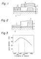
- Figure 1 is a cross section of a convention magnetic bubble memory chip;
- Figure 2 is a cross-section of a conventional bubble memory chip at one step in its production;
- Figure 3 is a graph illustrating the relationship between the thickness of a spacer in a magnetic bubble memory chip and the bias margin characteristics of the chip;
- Figures 4A to 4F are a series of cross-sections through a magnetic bubble memory chip illustrating the process for manufacturing it in accordance with the present invention;
- Figure 5 is a plan of a magnetic bubble memory chip manufactured in accordance with the present invention;
- Figure 6 is a plan of the minor loop organization and areas adjacent to its gates;
- Figure 7 and 8 are plans of the shapes of soft magnetic patterns used in the first and second areas respectively.
- Figure 1 illustrates a cross-section of a magnetic bubble memory chip having a dual spacing layer structure manufactured in accordance with a prior art technique, and Figure 2 illustrates an enlarged cross-section of the bubble memory chip of Figure 1 during the manufacturing process. According to the known art, a layer of
Si0 2 2 is formed on agarnet film 1 by sputtering and gold (Au)conductive patterns 3 for controlling function gates are formed thereon. In order to level the steps of theconductive pattern 3, a high temperaturetolerant resin 4, such as polyladder-organosiloxane (PLOS), is coated thereon and thermoset, and then only thePLOS layer 4 in an area.5 of the chip corresponding to the small-sized transmission patterns for the information accommodating section is etched, with a plasma etching agent including CF 4 etchant gas.Permalloy patterns 6 for the transmission patterns are then formed on the etched region. - The above-mentioned prior art method has several problems. First is the unevenness of the rate of etching in each batch when manufacturing the magnetic bubble memory chips. Conventionally, a plannar plate type etching machine is generally used for etching such a high temperature
tolerant resin 4, and although this type of etching machine is superior to a cylindrical type etching machine in etching evenness, usually there is still a variation in the rate of etching of within ±5% per one batch. For instance, if the film thickness of the high temperaturetolerant resin layer 4 is 3800 A and the 0 thickness is to be reduced by etching by 3000 A, to 0 obtain a spacer having a thickness of 1300 A including 0 the SiO2 layer 2 of 500 A, a variation of etching within ±150 A will occur per one batch when thickness of the 0 high temperature tolerant resin is reduced by 3000 A. In addition, when variation between the batches are taken into account, there may be a variation of at least ±300 0 0 A. Such a large variation of ±300 A will cause a serious problem, i.e. degradation of performance of the bubble memory chip, since 1300 A is the most favourable thickness for a spacer, as will be described hereinafter. - Second is when an
uneven face 7 having a thickness 0 0 of 200 A to 300 A is formed on the etched surface, as seen from Figure 2, the permalloy film formed thereon may have a local high spot Hc, which will affect the characteristics of the bubble memory. Figure 3 shows the relationship between the thickness of the spacer and the bubble propagation performance when using a soft magnetic pattern having 4 µm pattern periods. As can be seen in the figure, a o thickness of 1300 A ensures the most favourable relationship. - Figures 4A to 4F sequentially illustrate the respective steps in a process of manufacturing a magnetic bubble memory chip according to the present invention. In Figures 4A to 4F,
reference numeral 10 denotes a thin garnet film of a magnetic bubble; 11, a first insulative layer; 12, a conductive pattern for controlling function gates; 13, a second insulative layer; 14, a first area; 15, a second area; 16, a photoresist layer; 17, a third insulative layer; and 18 and 18', soft magnetic patterns for bubble transmission. - An embodiment of a process for manufacturing a magnetic bubble memory chip according to the present invention will now be described with reference to Figures 4A to 4F.
- In a first step, as shown in Figure 4A, a first
insulative layer 11 is formed by sputtering SiO2 to a o _ 500 A thickness on a magnetic bubblethin film 10 formed on a substrate. - In a second step, as shown in Figure 4B, a function gate controlling conductor consisting of Au, at a 0 thickness about 3500 A, is formed on the first
insulative layer 11 by vapour deposition, and then a function gate controllingconductive pattern 12 is formed by sputtering with a photolithographic method. In this case, TaMo 0 0 having a thickness 100 A to 150 A also can be used to improve the adhesiveness of theAu conductor 12 to the SiO2insulative layer 11. - In a third step, as shown in Figure 4C, a polyladderorganosiloxane resin (PLOS) having a thickness 0 of 2600 A, is coated over the whole surface and thermoset to form a second
insulative layer 13. - In a fourth step, as shown in Figure 4D, the
second area 15 of this chip is covered with aresist 16. On the other hand, in thefirst area 14 of this chip which will serve as an information accommodating section, the first and secondinsulative layers thin film 10 in thefirst area 14 of the magnetic bubble memory chip. In this case, both the first and second insulative layers of SiO2 and PLOS resin can be etched with the same etchant, since a main component of PLOS is Si. - In a fifth step, as shown in Figure 4E, a third
insulative layer 17 of SiO2, having a thickness of 1300 A, is formed by sputtering over the first 14 and second 15 areas. As seen from Figure 3, the thickness of theinsulative layer 17 is favourably 1200 A to 1500 A, 0 most preferably 1300 A. - At the sixth and final step, as shown in Figure 4F, after a soft magnetic material, such as permalloy, is formed by vapour deposition on the third
insulative layer 17, softmagnetic patterns 18 and 18' for bubble transmission, having different pattern periods, are formed thereon by photolithography or ion-etching. In this case, the softmagnetic pattern 18 constitutes transmission lines in the minor-loop organization in thefirst area 14 and the pattern period thereof is, for example, 4 µm to 6 µm. On the other hand, the soft magnetic pattern 18' constitutes major transmission lines and a pattern for connecting the major transmission lines to the minor-loop organization, and the pattern period thereof is, for example, 8 µm to 16 µm. - According to the illustrated embodiment, since the magnetic bubble
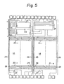
thin film 10 is not etched at all with the plasma etching agent using CF4, a slight overetching is effective to prevent any nonuniformity of the etching and variations of the etched layer thickness. Therefore, magnetic bubble memory chips having a stable propagation performance can be obtained. - Figure 5 is a plan view of an embodiment of a magnetic bubble memory chip manufactured in accordance with the present invention. In Figure 5, reference numerals 20-1 to 20-n and 21-1 to 21-n denote minor-loops organization; 22 and 23, boot loops for memorizing information concerning faulty loops in the minor-loop organization; 24, detectors; 25, recording major lines; 26, read out major lines; 27, generators; 28, swap-gates; and 29, replicate-gates.
- The embodiment shown in Figure 5 is an odd-and-even number type major-minor organization, in which the first area comprises the minor-loop organization 20-1 to 20-n and 21-1 to 21-n, which serve as an information accommodating section, and the
boot loops first area 14 uses small soft magnetic patterns 18 (Figure 4F) having 4 µm periods and the thickness of the spacer thereof is 1300 A, as seen from Figure 4F. - The area other than the
first area 14 is the second area, comprising, for instance, thegenerators 27, the recordingmajor lines 25, the read outmajor lines 26, the swap-gates 28, thereplicate gates 29, thedetectors 24, and some small portions of the minor loop organization adjacent to the gates. The second area is constituted by soft magnetic patterns of 8 µm to 16 µm periods and the thickness of the spacer thereof is 4400 A, as seen from Figure 4F. - Figure 6 is a plan view of the minor-loop organization and the areas adjacent to the gates thereof, in which
reference numeral 30 denotes a minor-loop organization; 25, recording major lines; 26, read out major lines; 28, swap-gates; and 29, replicate gates. In Figure 6, the area illustrated by hatching in theminor loop organization 30 is the first area. On the other hand, the area of a few bits adjacent to the gates using large softmagnetic patterns 35 for connecting is included in the second area. Also, as will be understood from Figure 6, the boundary portions between the first and second areas are defined by bubble transmission gaps between adjacent patterns of the respective areas. - Figures 7 and 8 illustrate soft magnetic patterns used for the transmission lines in the minor loop organization 30 (Figure 6) in the first area, and for the patterns 35 (Figure 6) in the second area, respectively. The pattern illustrated in either Figure 7 or 8 is a so-called "Wide Gap" pattern, which has more advantages in size and in the possibility of high density loading than the half disk pattern or asymmetrical chevron pattern conventionally used in the prior art, since the gap spacing of the former is larger than that of the latter.
- As discussed hereinbefore in detail, a method for manufacturing a magnetic bubble memory chip according to the present invention is particularly advantageously adopted when manufacturing a dual-spacing layer structure or dual spacing type bubble chip consisting of thin and thick layers. Consequently, according to the present invention, when the thin layer is formed, the unevenness of etching and variations in thickness thereof are prevented, so that magnetic bubble memory chips having stable bubble propagation performance and characteristics with less variations can be obtained.
Claims (7)
Applications Claiming Priority (2)
| Application Number | Priority Date | Filing Date | Title |
|---|---|---|---|
| JP39741/84 | 1984-03-03 | ||
| JP59039741A JPS60185289A (en) | 1984-03-03 | 1984-03-03 | Production of magnetic bubble memory element |
Publications (3)
| Publication Number | Publication Date |
|---|---|
| EP0154524A2 true EP0154524A2 (en) | 1985-09-11 |
| EP0154524A3 EP0154524A3 (en) | 1986-10-01 |
| EP0154524B1 EP0154524B1 (en) | 1989-11-08 |
Family
ID=12561386
Family Applications (1)
| Application Number | Title | Priority Date | Filing Date |
|---|---|---|---|
| EP85301400A Expired EP0154524B1 (en) | 1984-03-03 | 1985-02-28 | Process for manufacturing a magnetic bubble memory chip |
Country Status (6)
| Country | Link |
|---|---|
| US (1) | US4579624A (en) |
| EP (1) | EP0154524B1 (en) |
| JP (1) | JPS60185289A (en) |
| KR (1) | KR900000046B1 (en) |
| CA (1) | CA1219969A (en) |
| DE (1) | DE3574200D1 (en) |
Families Citing this family (1)
| Publication number | Priority date | Publication date | Assignee | Title |
|---|---|---|---|---|
| US4693780A (en) * | 1985-02-22 | 1987-09-15 | Siemens Aktiengesellschaft | Electrical isolation and leveling of patterned surfaces |
Citations (4)
| Publication number | Priority date | Publication date | Assignee | Title |
|---|---|---|---|---|
| JPS578986A (en) * | 1980-06-19 | 1982-01-18 | Nec Corp | Manufacture of magnetic bubble element |
| JPS5783014A (en) * | 1980-11-12 | 1982-05-24 | Hitachi Ltd | Manufacture of magnetic bubble memory |
| JPS5796516A (en) * | 1980-12-09 | 1982-06-15 | Fujitsu Ltd | Manufacture of bubble memory chip |
| JPS57122508A (en) * | 1981-01-23 | 1982-07-30 | Nec Corp | Manufacture magnetic bubble device |
-
1984
- 1984-03-03 JP JP59039741A patent/JPS60185289A/en active Granted
-
1985
- 1985-02-26 CA CA000475171A patent/CA1219969A/en not_active Expired
- 1985-02-28 DE DE8585301400T patent/DE3574200D1/en not_active Expired
- 1985-02-28 EP EP85301400A patent/EP0154524B1/en not_active Expired
- 1985-02-28 US US06/706,612 patent/US4579624A/en not_active Expired - Fee Related
- 1985-03-02 KR KR1019850001315A patent/KR900000046B1/en not_active IP Right Cessation
Patent Citations (4)
| Publication number | Priority date | Publication date | Assignee | Title |
|---|---|---|---|---|
| JPS578986A (en) * | 1980-06-19 | 1982-01-18 | Nec Corp | Manufacture of magnetic bubble element |
| JPS5783014A (en) * | 1980-11-12 | 1982-05-24 | Hitachi Ltd | Manufacture of magnetic bubble memory |
| JPS5796516A (en) * | 1980-12-09 | 1982-06-15 | Fujitsu Ltd | Manufacture of bubble memory chip |
| JPS57122508A (en) * | 1981-01-23 | 1982-07-30 | Nec Corp | Manufacture magnetic bubble device |
Non-Patent Citations (9)
| Title |
|---|
| Majima et al., IEEE TRANSACTIONS ON MAGNETICS, Vol. MAG-20 No. 5, September 84, pages 1066-1071 * |
| PATENT ABSTRACTS OF JAPAN, vol. 6, no. 164 (E-127)[1042], 27th August 1982; & JP-A-57 083 014 (HITACHI EISAKUSHO K.K.) 24-05-1982 * |
| PATENT ABSTRACTS OF JAPAN, vol. 6, no. 182 (E-131)[1060], 18th September 1982; & JP-A-57 096 516 (FUJITSU K.K.) 15-06-1982 * |
| PATENT ABSTRACTS OF JAPAN, vol. 6, no. 218 (E-139)[1096], 2nd November 1982; & JP-A-57 122 508 (NIPPON DENKI K.K.) 30-07-1982 * |
| PATENT ABSTRACTS OF JAPAN, vol. 6, no. 70 (P-113)[948], 6th May 1982; & JP-A-57 008 986 (NIPPON DENKI K.K.) 28-01-1982 * |
| PATENTS ABSTRACTS OF JAPAN, vol. 6, no. 164 (E-127)[1042], 27th August 1982; & JP - A - 57 83 014 (HITACHI EISAKUSHO K.K.) 24-05-1982 * |
| PATENTS ABSTRACTS OF JAPAN, vol. 6, no. 182 (E-131)[1060], 18th September 1982; & JP - A - 57 96 516 (FUJITSU K.K.) 15-06-1982 * |
| PATENTS ABSTRACTS OF JAPAN, vol. 6, no. 218 (E-139)[1096], 2nd November 1982; & JP - A - 57 122 508 (NIPPON DENKI K.K.) 30-07-1982 * |
| PATENTS ABSTRACTS OF JAPAN, vol. 6, no. 70 (P-113)[948], 6th May 1982; & JP - A - 57 8986 (NIPPON DENKI K.K.) 28-01-1982 * |
Also Published As
| Publication number | Publication date |
|---|---|
| KR850007151A (en) | 1985-10-30 |
| US4579624A (en) | 1986-04-01 |
| JPS60185289A (en) | 1985-09-20 |
| DE3574200D1 (en) | 1989-12-14 |
| EP0154524A3 (en) | 1986-10-01 |
| CA1219969A (en) | 1987-03-31 |
| EP0154524B1 (en) | 1989-11-08 |
| JPS6336069B2 (en) | 1988-07-19 |
| KR900000046B1 (en) | 1990-01-18 |
Similar Documents
| Publication | Publication Date | Title |
|---|---|---|
| US4841624A (en) | Method of producing a thin film magnetic head | |
| US4246620A (en) | Thin film magnetic head and method for manufacturing the same | |
| US4703383A (en) | Coil conductor structure in thin-film magnetic head | |
| CN1087494C (en) | Contact mask for manufacturing semiconductor device | |
| EP0068846A1 (en) | Forming a pattern of metal elements on a substrate | |
| EP0154524B1 (en) | Process for manufacturing a magnetic bubble memory chip | |
| JPH0380410A (en) | Thin-film magnetic head and production thereof | |
| JP2705253B2 (en) | Conductive pattern forming method and magnetic head manufacturing method | |
| US4701767A (en) | Magnetic recording head and method for manufacturing | |
| JP2747099B2 (en) | Thin film magnetic head | |
| US4607349A (en) | Magnetic bubble memory device | |
| JPH09138910A (en) | Method of patterning metal layer | |
| JPH05314448A (en) | Bonding pad and forming method of bonding pad section | |
| JPH0126176B2 (en) | ||
| JPS641876B2 (en) | ||
| JPH03125307A (en) | Manufacture of this film magnetic head | |
| JPH05182135A (en) | Thin-film magnetic head and production thereof | |
| JPS63201908A (en) | Production of thin film magnetic head | |
| JPS6111915A (en) | Production of thin film magnetic film | |
| JPH03100910A (en) | Thin-film magnetic head | |
| JPH0281309A (en) | Thin-film magnetic head and its production | |
| JPH02308407A (en) | Production of thin-film magnetic head | |
| JPS62205509A (en) | Thin film magnetic head | |
| JPS63103409A (en) | Thin film magnetic head | |
| JPS6370992A (en) | Manufacture of magnetic bubble memory element |
Legal Events
| Date | Code | Title | Description |
|---|---|---|---|
| PUAI | Public reference made under article 153(3) epc to a published international application that has entered the european phase |
Free format text: ORIGINAL CODE: 0009012 |
|
| AK | Designated contracting states |
Designated state(s): DE FR GB NL |
|
| PUAL | Search report despatched |
Free format text: ORIGINAL CODE: 0009013 |
|
| AK | Designated contracting states |
Kind code of ref document: A3 Designated state(s): DE FR GB NL |
|
| 17P | Request for examination filed |
Effective date: 19870313 |
|
| 17Q | First examination report despatched |
Effective date: 19880525 |
|
| GRAA | (expected) grant |
Free format text: ORIGINAL CODE: 0009210 |
|
| AK | Designated contracting states |
Kind code of ref document: B1 Designated state(s): DE FR GB NL |
|
| ET | Fr: translation filed | ||
| REF | Corresponds to: |
Ref document number: 3574200 Country of ref document: DE Date of ref document: 19891214 |
|
| PLBE | No opposition filed within time limit |
Free format text: ORIGINAL CODE: 0009261 |
|
| STAA | Information on the status of an ep patent application or granted ep patent |
Free format text: STATUS: NO OPPOSITION FILED WITHIN TIME LIMIT |
|
| 26N | No opposition filed | ||
| PGFP | Annual fee paid to national office [announced via postgrant information from national office to epo] |
Ref country code: FR Payment date: 19940210 Year of fee payment: 10 |
|
| PGFP | Annual fee paid to national office [announced via postgrant information from national office to epo] |
Ref country code: GB Payment date: 19940218 Year of fee payment: 10 |
|
| PGFP | Annual fee paid to national office [announced via postgrant information from national office to epo] |
Ref country code: DE Payment date: 19940224 Year of fee payment: 10 |
|
| PGFP | Annual fee paid to national office [announced via postgrant information from national office to epo] |
Ref country code: NL Payment date: 19940228 Year of fee payment: 10 |
|
| PG25 | Lapsed in a contracting state [announced via postgrant information from national office to epo] |
Ref country code: GB Effective date: 19950228 |
|
| PG25 | Lapsed in a contracting state [announced via postgrant information from national office to epo] |
Ref country code: NL Effective date: 19950901 |
|
| GBPC | Gb: european patent ceased through non-payment of renewal fee |
Effective date: 19950228 |
|
| PG25 | Lapsed in a contracting state [announced via postgrant information from national office to epo] |
Ref country code: FR Effective date: 19951031 |
|
| NLV4 | Nl: lapsed or anulled due to non-payment of the annual fee |
Effective date: 19950901 |
|
| PG25 | Lapsed in a contracting state [announced via postgrant information from national office to epo] |
Ref country code: DE Effective date: 19951101 |
|
| REG | Reference to a national code |
Ref country code: FR Ref legal event code: ST |