EP0146875A2 - Röntgenstrahlgenerator mit Spannungsregelkreis - Google Patents
Röntgenstrahlgenerator mit Spannungsregelkreis Download PDFInfo
- Publication number
- EP0146875A2 EP0146875A2 EP84115236A EP84115236A EP0146875A2 EP 0146875 A2 EP0146875 A2 EP 0146875A2 EP 84115236 A EP84115236 A EP 84115236A EP 84115236 A EP84115236 A EP 84115236A EP 0146875 A2 EP0146875 A2 EP 0146875A2
- Authority
- EP
- European Patent Office
- Prior art keywords
- voltage
- inverter
- output
- control
- generator
- Prior art date
- Legal status (The legal status is an assumption and is not a legal conclusion. Google has not performed a legal analysis and makes no representation as to the accuracy of the status listed.)
- Withdrawn
Links
Images


Classifications
-
- H—ELECTRICITY
- H05—ELECTRIC TECHNIQUES NOT OTHERWISE PROVIDED FOR
- H05G—X-RAY TECHNIQUE
- H05G1/00—X-ray apparatus involving X-ray tubes; Circuits therefor
- H05G1/08—Electrical details
- H05G1/26—Measuring, controlling or protecting
- H05G1/30—Controlling
- H05G1/32—Supply voltage of the X-ray apparatus or tube
Definitions
- This invention relates generally to X-ray-generation systems and, more particularly, to a voltage-feedback network for the control of the output voltage to an X-ray tube.
- a typical voltage level that may be applied in conventional radiography might be in the range of 50 kv to 150 kv, whereas in a fluorographic application the voltage is more likely to be in the 50 kV to 120 kV range, and for use in mammographic X-ray applications it is more likely to be in the range between 24 kV and 50 kV.
- the level of current which is applied may vary from 0.1 mA for fluorographic applications to 1250 mA for certain radiographic procedures.
- the conventional approach for maintaining a substantially constant voltage level with the variations that may occur in the line is to use the so-called volt-pac which is a variable input/output transformer driven by a motor to obtain a variable output.
- a primary disadvantage of the volt-pac is that it is relatively slow in operation, i.e., the volt-pac has a response time of about 1 second. For this reason, the volt-pac control is used only to set up the correct voltages at the start of exposure and is not thereafter adjusted except during long (i.e., fluoroscopic) exposures. This is to be compared with a desired response time in the millisecond range for an X-ray generator system which is able to provide a short power pulse of good definition for a large variety of procedures and applications.
- a high-voltage pulse with a very quick rise time, i.e., as short as 1 millisecond, a flat peak for an exposure as short as 1 millisecond, and a quick fall time. Hence, corrections need to be accomplished in less than one millisecond.
- phase-controlled rectifiers transistor series or shunt regulators
- semi-conductor switching-type d.c. voltage controls to name a few.
- the semi-conductor switching device commonly known as the chopper can generally provide more efficient and faster response d.c. voltage controls than the other techniques.
- the substantial filtering requirement in the d.c. circuit it is much too slow in response time for operation in a complete closed-loop voltage regulated inverter power supply.
- Another object of the present invention is the provision in an X-ray generator system for a closed-loop voltage feedback loop which is effective for rapidly and accurately responding to fluctuations in the input voltage and in the load so as to maintain the desired voltage output.
- Yet another object of the present invention is the provision in an X-ray generator system for a control network which is sufficiently fast and responsive over a wide range of operating conditions to provide a generated power pulse having a rapid rise time followed by a relatively short exposure time of substantially constant voltage, and a relatively fast fall time.
- an X-ray generation system is provided with a high-voltage feedback from the tube, and a control network which is responsive to that feedback to control the operation of the system inverter in such a way as to maintain a predetermined voltage level to the X-ray tube.
- the feedback signal is applied to directly control the output of the inverter so that the system can quickly and accurately respond to variations in both the line voltage and the load.
- the cooperating components such as the high-voltage transformer, high-voltage output filter, and high-voltage bleeder circuitry, are designed to be compatible with, and contribute to, the quick response features of the system.
- the resulting control network provides a system which is capable of providing to the X-ray tube a high voltage output which has: a rise time as short as one millisecond; a steady-state, high-voltage period as short as one millisecond with minimal ripple; and a fast fall time, particularly for very low mAs such as 0.25 mAs.
- a transistor inverter operating at relatively high frequencies is adapted to provide a square wave, pulse-width-modulated output whose rectified output voltage level is controlled by selectively varying, not only the mark/space ratio, but also the frequency of the output waveform.
- the inverter is controlled in response to: operator settings; the output voltage feedback; and to generated signals representative of certain operating conditions of the system.
- Another aspect of the invention relates to the sensing of a saturating condition in the transformer core and for responsively initiating corrective action to alleviate the problem.
- Means are provided to sense the current in the transformer and to integrate the resulting signal to obtain an indication of an approaching core-saturation condition.
- the signal is then applied to a sawtooth generator to generate control signals which act to selectively unbalance the current flow in the two diagonals in such a way as to alleviate the saturating condition.
- a phase-advance network is included to dynamically vary the gain of the system in such a way as to provide for a high gain during the initial stage so as to obtain a short rise time, while subsequently reducing the gain so as to clamp the kV overshoot at the end of the rise time.
- This effect is provided by applying the voltage feedback signal to a phase-advance circuit prior to its being applied to the voltage demand signal at the input to an amplifier.
- the attendant noise that is introduced by the phase-advance network is alleviated by a phase-lag network which is provided in the feedback loop of the amplifier.
- a high-voltage divider circuit is provided to obtain a low-voltage control signal representative of the output voltage for use in the control network.
- the filter capacitor is used for that purpose and, as such, is useful in a dual-purpose mode. This leads to a substantial reduction in the number of conponents and, when used with the present high-frequency pulse-width-modulated output, provides a closed-loop voltage-feedback system with good transient response.
- a microprocessor is incorporated to monitor the system and, on the basis of status signals which it receives, to modulate the system operation and/or shut down the system accordingly.
- Some of the specific conditions against which the protection system acts to reduce, prevent, or stop the system operation are: over-voltage at the output, unbalance between the anode and the cathode with respect to ground, excessive current flow, and excess of kilovolt uncontrolled demand. Provision is also made to begin timing of X-ray exposures only after the output voltage level has reached 75% of the demand or equipment set point, thereby ensuring improved performance, and meeting prescribed regulations.
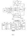
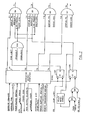
- FIG. 1 A typical prior-art X-ray generator system is shown in FIG. 1 to comprise a three-phase power source 11, connected by way of an autotransformer 12, to the three-phase transformer 13.
- the autotransformer 12 includes taps 14 that can be selectively varied with respect to the primary coil 16 so as to vary the connection of the primary to the incoming line to thereby compensate for varying line conditions.
- the power transformer 13 will typically have a Y-primary 17 and a A Y-connected secondary winding 1B, producing an output waveform with either 12 or 6 pulses. The outputs are then connected to full-wave rectifier bridges 19 and 21, which in turn provide high voltage to the X-ray tube 22.
- the power level to the X-ray tube 22 is varied by way of the variable input/output transformer 13, whose primary windings 17 are selectively closed by way of static contactors 23, normally by way of SCR I S .
- Such a conventional system is subject to the various disadvantages discussed hereinabove.
- the X-ray generator system of the present invention is shown in FIG. 2 to comprise a three-phase power source 23, an a.c. to d.c. three-phase non-controlled rectifier 24, an LC filter 26, and a d.c. to a.c. pulse-width modulator inverter 27 operating at variable high-frequency conditions, i.e., in the range of several kilohertz.
- the output of the inverter 27 is controlled by way of pulse-width modulation with provisions for varying both the mark-space ratio and the frequency by way of a kVp feedback controller, as will be described more fully hereinafter.
- the output from the PWM inverter 27 passes to a high-tension transformer 28, through a single-phase rectifier 29 and is finally applied to an X-ray tube 31.
- the present invention provides for such a wide range of operating conditions and performance parameters by controlling the X-ray output in a fast and accurate manner, as will -be described in more detail hereafter. It will be seen by reference to the FIG.
- a primary feature of this fast response system is the closed-loop feedback control which senses, by way of the voltage divider 32, the voltage across the X-ray tube 31 and provides a representative signal to the high-voltage feedback control 33, which in turn provides a control signal to the PWM inverter 27.
- the power source is described as a three-phase input, it may as well be a single-phase input. Since the system of the present invention is designed to operate at frequencies which are substantially higher than those of a conventional generator, the complications of wave-form ripple are substantially reduced. For this reason, where single-phase operation is not practical in a conventional X-ray generator, it is practical when used with the acconnodating features of the present invention.
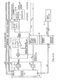
- FIGS. 3A and 3B The square-wave pulse-width-modulated inverter and control system of the present invention is shown schematically in FIGS. 3A and 3B as comprising the following elements: a Central Control Microprocessor Kilovolts Demand Control 33, omploying a microprocessor 30; a Mixer Amplifier and Feedback Controller 34; a Sawtooth Generator and Comparator 36; a Logic Controller Unit 37; Power Transistor Controllers 38; the square-wave pulse-width modulated transistor inverter 27; an Inverter Monitor 40 with its dedicated microcomputer 41 which controls the interlock for safety signals from the power transistor inverter 27 back to the Logic Controller Unit 37; the high voltage transformer 28; the high voltage rectifier 29; the High Voltage Bleeder 32; a High Voltage Divider Feedback Circuitry 46; an Antisaturation Circuit 47 which works with the error signal and the Sawtooth Generator and Comparator 36; a Current Limit Circuit 48; a Display Console and operator controls 49, with its installed microprocessors; and an Imaging
- the overall control system is coordinated by the microcomputer 41 and control microprocessor 30, the inverter microcooputer 41 being dedicated to continuously monitor and check the high voltage power transistor inverter 27 and the central control microprocessor 30 acting to control the demand prior to and during exposure.
- the control microprocessor 30 also reads the kilovolts coming from the feedback to provide, during exposure, an accurate control of what is happening on the high voltage side.
- Any of a number of commercially available microprocessors and/or microcomputers may be used with the present invention.
- the Intel 8085 microprocessor may be used for the central control function
- the Intel 8749 microcomputer may be employed for monitoring the inverter operation.
- the central microprocessor 30, in response to signals from the Display Console 49, generates the Kilovolts Demand and passes that signal, by way of the D/A converter 52, to the Mixer Amplifier and Feedback Controller 34.
- the Kilovolts Acknowledge signal comes to the central microprocessor 30 by way of the A/D converter 53.
- the Kilovolts Demand and Kilovolts Acknowledge signals should be maintained very close together and, in addition to being monitored by the central microprocessor 30 for that purpose, are also used as inputs for protection if, on the high voltage side, an arcing occurs or a component is damaged. In such case, the Kilovolts Demand signal will not be followed by the Kilovolts Acknowledge signal and the central microprocessor 30 will, therefore, shut down the system.
- the central microprocessor 30 is connected to Display Console 49 by a data link 54, to the inverter microcomputer 41 by lines 56 and 57 and to the High Voltage Feedback Circuits 46 by line 58.
- the data handling and communication starts at the Console 49 where the operator enters the exposure times and other parameters. Those parameters are analyzed and controlled by the system microprocessor, such as an Intel 8088 microprocessor, in conjunction with an arithmetic co-processor, such as an Intel 8087, which handles all of the arithmetical calculations for x-ray protection and exposure parameters.
- the Console 49 has the further capability of serving another data link 62 to the Image Systems 51 so that the communication is completely digital to provide high reliability during its operation.
- the communication between the central microcomputer 30 on the cabinet side and the inverter microcomputer 41 is also done in a bidirectional way by lines 56 and 57.
- the operator control state is such that kilovolts and exposure time are being provided to the central control microprocessor 30 and from there to the inverter microcomputer 41, which controls the output voltage during exposure, the inverter operation, and the exposure time, such that, during the X-ray exposure, there are three microprocessors controlling exposure time, (i.e., the centrol control microprocessor 30 and inverter microcomputer 41 on the cabinet side and, as a backup, the Display Console microprocessor 8088 on the console side.
- Such a combination provides redundant protection against an excessive dose of radiation during exposure.
- the Mixer Amplifier and Feedback Controller 34 produces a narrow signal which is the difference between the Kilovolts Demand and the Kilovolts Acknowledge or feedback.
- the resulting kV error signal is amplified and processed with phase advance and phase lag circuits, to be described more fully hereinafter, to make the system stable.
- the kV Error signal is then fed, along with a signal from the Antisaturation Circuit 47, to the Sawtooth Generator and Comparator 36.
- the signal from the Antisaturation Circuit 47 controls the slope of the sawtooth generator so as to prevent the high voltage transformer 28 from reaching a condition of saturation, as will be more fully described hereinafter.
- the kV Error Signal feeds the Sawtooth Generator and Comparator 36 to produce a PWM train of pulses with a variable mark/space ratio, which in turn is applied to control the output voltage and to adjust it automatically through the closed-loop kilovolt feedback operation.
- the Sawtooth Generator and Corrparator 36 and Logic Controller Unit 37 are controlled by a reset or synchronization signal received every half cycle along line 64 from the dedicated microprocessor 41 to guarantee that the kV Error Signal from the mixer 34 will intersect the sawtooth generator waveform once per half cycle to thereby avoid the possibility of having several intersections which might lead to problems at the power stage circuit.
- the Logic Controller Unit 37 which handles all of the system protections and timing, has, by way of fibre-optic line 66, an output which controls the power transistor inverter 27 through the Power Transistor Controllers 38.
- This Logic Controller Unit 37 also handles the Current Limit 48 output.
- the Current Limit Circuit 48 is responsive to the inverter current level, detected with a current transformer 67 in series with the primary of the high voltage transformer 28. The sensed current level is compared, in the Current Limit Circuit 48, with a predetermined safe level, and the output of the Current Limit Circuitry 48 is applied to the Logic Controller Unit 37 to cut off the mark/space pulses dynamically if a circuit overload condition occurs.
- the output from the current transformer 67 is also fed back into the Antisaturation Circuit 47, and its output, in turn, is applied to the sawtooth generator along line 74 to vary the slope dynamically to electronically compensate for saturations in the transformer.
- the Power Transistor Controller 38 In addition to providing signals to directly control the power transistor inverter 27, the Power Transistor Controller 38, also provides, along line 68, signals indicative of the power supply status on the controllers and of the transistor's status, back to the inverter microcomputer 41 which uses that information to control the Logic Controller Unit 37 such that, should any transistor or power supply fail, the information coming from the Transistor Controller 38 will be fed back, in real-time, into the Logic Contoller Unit 37 which will, first of all, stop the inverter and, secondly, will open the appropriate safety contactor(s) 63.
- the pulse-width-modulated inverter 27 is comprised of a plurality of transistors shown generally in FIG. 3 as T l -T 4 , arranged in a full bridge disposition so as to provide alternate conduction through the transformer primary 28 by way of diagonals T I -T 4 and T 2 -T 3 .
- the transistors may be used as shown or, alternately, may be used in parallel where the power requirements may require it.
- One type of transistor that has been found to be useful in the present invention is that identified by the designation WT-5752, which is commercially available from Westinghouse Brake (Westcode) in Chippenham England.
- the pulse-width modulation is affected by the selective turning on and off of the top transistors T 1 and T 2 only.
- the high voltage transformer 28 is described in U.S. Patent Application No. (15-XZ-2454), filed concurrently herewith and incorporated herein by reference. Suffice it to say, the transformer 28 is designed to have a very low leakage inductance so that the square waveform produced in the PWM inverter is pulsed to the secondary of the transformer with very good waveform reproduction. In this way, the drop between pulses is minimized and the ripple, after rectification, is kept to a minimum so as to thereby limit the size of the output filter. This, in turn, facilitates a high reproducibility operation at lower mAs settings.
- the rectifier 29 is of the conventional single-phase type.
- the High Voltage Divider or High Voltage Bleeder 32 is designed to include unique resistive and capacitive electronic circuitry, shown generally as 69, 71, 107, and 108, to improve the response of the transformer 28 to the dynamic variations of the load or source, or to other transient conditions, such that the rise and the fall times are minimized.
- the output from the High Voltage Bleeder 32 is the Kilovolts Output which feeds, along line 72, to the High Voltage Divider Feedback Circuits 46 in a step-down voltage fashion.
- the operation of the closed-loop kV feedback system is primarily dependent on the Mixer Amplifier and Feedback Controller 34, which produces an error signal equal to the difference between the Kilovolts Demand and the Kilovolts Output. It is necessary for the Controller 34 to (1) be conditioned to the electronic circuitry level through the high voltage divider feedback circuits so that the error signal generates a mark/space train of pulses with the specific ratio depending on the kilovolts' demand, and (2) compensate for the three main variables which may disturb the system operation during exposure, the variables being (a) the fixed d.c.
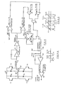
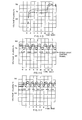
- FIG. 4 there is shown a schematic illustration of the combination of the Antisaturation Circuit 47 (FIG. 3) and the Sawtooth Generator and Comparator 36 in combination.
- the Sawtooth Generator and Corparator 36 is responsive to three signals: (1) the synchronization signal which canes in on line 64 to reset the sawtooth range every half cycle; (2) the control signal which is fed, on line 73, directly to the Sawtooth Generator 36 from the Antisaturation Circuit 47; and (3) the Kilovolts Error Signal E from Mixer Amplifier 34.
- the Antisaturation Circuit 47 is responsive to the current output of the inverter as received along line 74.
- the inverter is shown to include transistors T 1 -T 4 with associated flywheel diodes D 1 -D 4 .
- the current in the inverter or primary of the transformer 28 is sensed by current transformer 67 and is passed on line 74 to an integrator 76 whose output in turn passes on line 77 to an error amplifier 78 whose output is applied to two comparators 79 and 81.
- These comparators have respective positive and negative reference levels which normally are of very low value, i.e., nearly zero, and fix what is called the admissible saturation level in the transformer. It will be seen that the respective outputs from the comparators 79 and 81 are applied to NAND Gates Gl and G2, whose outputs are applied to NAND Gate G3.
- the output from NAND Gate G3 acts to close an FET switch F1 on either one diagonal T 1 , T 4 or the other T 2 , T 3 in the power inverter.
- a closing of the FET switch Fl will allow the Error Amplifier output signal, which is proportional to the current sensed, to feed a precision rectifier 82 working in the first and fourth gradients which in turn feeds a linear output through the FET switch F1, to the sawtooth generator or compensator.
- the sawtooth generator is an integrator 83 which is preset by the synchronization signal from line 64 and produces a sawtooth whose slope is set for a zero saturation level constant as shown in FIGS. 5A and 5B and defined by the range of a part of the overall closed-loop feedback system.
- the sawtooth waveform signal is then applied, along with the kV Error Signal E, to a comparator 85 which responsively generates a PWM train of pulses that controls the inverter.
- the error amplifier 78 will produce a d.c. level input to the precision rectifier 82 whose output will be linearly proportional to the irput. It will be recognized that the precision rectifier 82 is responsive to either positive or negative d.c. volts input from the error amplifier 78, with the sign being dependent on the applicable current direction in the power transistor inverter. Consequently, the magnitude of the particular d.c. saturation level determines the output of the precision rectifier 82, and that output in turn is passed through FET switch Fl, if the saturation level reaches above the preset reference levels to correct for the condition.
- the sawtooth generator will increase the slope on that part of the waveform when the T 1 , T 4 diagonal is conducting, and, as will be seen in FIG. SB, this increasing of the slope will lead to a decreasing in the mark/space ratio for a given error signal from the feedback, which in alternate cycles will decrease the mark/space ratio on that diagonal and will compensate dynamically for the difference in, say, hysteresis time in the transistors or unbalancements due to local saturations in the core.
- the output from the error amplifier will overcome the positive reference value on comparator 79 which in turn will send a camnand logic signal to NAND Gate G2 to synchronize with the on-time for the T 1 , T 4 diagonal so that, when the T 1 T 4 diagonal of transistors is turned on, the waveform of the sawtooth generator is automatically increased in slope and the mark/space ratio is diminished.
- the saturation level is dynamically and electronically compensated for by way of a closed-loop proportional control, i.e., the mark interval X is reduced and the interval Y is increased.
- the Logic Controller Unit 37 works in conjunction with the microcomputer 41, and will now be described in terms of both its analog and its digital functions.
- the analog functions are shown in FIG 6 and the flow of logic signals are shown in FIG. 7.
- Both the analog and the digital signal processing circuits result in outputs which are fed to the microcomputer 41, which in turn controls the overall inverter functions, protections, and performance operation.
- FIG. 6 there is shown on the left a series of input signals fran I 11 to I 6 and on the right a series of output signals from O 1 to 0 6 which are, respectively, applied to and result from the protection circuits in the system to control the overall system operation on the high voltage side.
- the anode and cathode-to-ground signals, I 11 and I 12 come from the voltage divider or bleeder 32 as will be seen by reference to FIGS. 3B and 8.
- These signals are added together in an operational amplifier 84 whose output is representative of the kV high voltage output. That output is fed back to the master or central microprocessor 30 in the cabinet to check, as is shown in FIG. 3, the kilovolt value in real-time operation.
- the output of operational amplifier 84 is fed into the positive side of an operational amplifier 86 where it is compared with the Kilovolts Demand signal I 2 which canes from the central microprocessor 30 in the power cabinet through a D/A converter 52 as shown in FIG. 3.
- the operational amplifier 86 calculates the error signal E of the kilovolts feedback and that signal is applied to the comparator 85 where it is compared with the output from the sawtooth generator as shown in FIGS. 4 and 5 to provide an output O 1 which is a pulse-width-modulated train of pulses which controls the inverter.
- FIG. 6 there are several different kinds of protective circuits which protect not only the high voltage side including the transformer 28 but also the power transistor inverter 27 and the related control circuitry which may be effected by the arcing, flashes, or transients which comonly cane from the high voltage side and are typical in all X-ray machines.
- Coaparator 88 output O 2 provides an over-voltage protection which: (1) is very fast in operation, and (2) is responsive to any small transient which might occur on the high voltage side.
- the kV demand 1 2 from the central microprocessor on the cabinet is fed to the positive input of the operational amplifier 89 and is added to a reference signal which is considered to be the maximum allowed overvoltage, for example, 10 kilovolts.
- the output from operational amplifier 89 is a signal which is the demand of kV plus 10 kilovolts, and that signal is then subtracted, or compared, in comparator 88 with the high voltage kV feedback signal which comes from operational amplifier 84 to feed the negative input of conparator 88.
- the output 0 2 from the comparator 88 will be logic 1 or logic zero, and the jump from logic zero to logic 1 is an over-voltage indication which will force the dedicated inverter microcomputer 41 to shut down the system through a software subroutine.
- This over-voltage feature once it is detected, trips or stops the inverter in a time as short as 10 microsec., which is 1000 - 2000 times faster than an over-voltage response in a conventional system. This feature will therefore protect and increase the life of an X-ray tube, the high tension rectifier 29, and the high voltage transformer 28 which in turn will have to withstand the overvoltage for only a few microseconds.
- FIG. 6 Another protection feature shown in FIG. 6 is that for unbalance between the difference of voltage between the anode-to-ground and the cathode-to-ground in the X-ray tube high voltage circuit. This is accomplished through operational amplifier 91 having inputs I 11 , I 12 , which inputs are subtracted to provide an output which is applied to a carparator 92 and compared with a 5 kilovolt reference signal. Should the unbalance between anode to ground and cathode to ground be greater than 5 kilovolts, comparator 92 will trip off, and the output 0 3 will immediately cause the inverter microcomputer 41 to shut down the system.
- This protection circuit has the capability of detecting a possible manufacturing defect in the secondary coils, i.e., should the secondary number of turns be in error so as to cause a difference of more than 5 kilovolts, then the error will be detected during a test by way of the circuit just described.
- the output difference will be greater than 5 kilovolts and this abnormality, which might be a fault situation, will be detected through the output of the window comparator 92, and a representative logic signal will be sent through the data link to the operator console.
- the protection of conparator 9 2 detects any failure, damage, or deviation, which might occur either in the secondary transformer coils, in the high tension rectifier, in the output filter, or in the X-ray tube itself.
- a protection circuit is that relating to the fact that, when a film is exposed to X-rays, most of the exposure is made when the power level is above 75% of the kV Demand level.
- a comparator 93 is provided and has as inputs the kV feedback signal at the positive input and, at the negative input, a signal representative of a 75% kV demand level which is derived by the operational amplifier 90 and voltage divider 95.
- the comparator 93 trips on to provide an output 0 4 , to thereby indicate to the dedicated microcomputer 41 that the 75% level of the kV demand has been reached and that the exposure time should now be counted.
- a related protective function of this circuit is that of detecting, during the rise time of the kilovolts, any fault in either the power transistor inverter 27 or in the integrated electronics, so that, if after a specified interval of time, for example, 2.5 msec., the kV feedback voltage does not reach the 75% of demand, it is assumed that there is a problem in the power transistor inverter 27, its peripheral electronics, the high voltage transformer 28, the rectifier 29, the filter, or the feedback circuits. This signal is then used to safely trip off the system.
- the three protection circuits described above all relate to the sensing of deviations in the voltage levels. There is also a need to provide for the sensing of, and protection against, the occurrence of excessive current levels. For that purpose, there are provided, as shown at the bottom of FIG. 6, two identical circuits called First Current Limit and Second Current Limit which are intended for redundancy but which have the same set-up levels.
- the reason for using redundant circuits is that, if an overload occurs, the inverter 27 will try to introduce higher current, and, therefore, there must be sane way of preventing the inverter from doing that. Such an overload might occur from a flash in the tube or might occur because there is an arc in the transformer or a short circuit in the output diodes, for example.
- the Current Limit network consists of two redundant circuits with the same set-up levels to sake sure that the system will be protected against failure of one of the Current Limit channels.
- the current limit is initiated through a pair of current transformers 94 and 96 having ferrite cores and being placed in series with the primary of the transformer 28 on the inverter output.
- the respective outputs are fed to the differential amplifiers 97 and 98 which have very high common mode rejection to avoid any noise such as may cane from the inverter, from radiation, etc.
- the outputs 1 5 and 1 6 are applied to the respective precision rectifiers 99 and 101 which produce DC level signals proportional to the respective currents, with nearly no delay. This is to be contrasted with the conventional use of an RC filter approach where the delay can be so long as to make the system not fully safe in terms of full response for the current limit operation.
- the outputs of the precision rectifiers 99 and 101 are applied to the positive inputs of the respective comparators 102 and 103.
- the two-current limit levels are applied to the negative inputs of the respective comparators 102 and 103.
- the outputs, 0 5 or 0 6 will trip off and will be applied, as will be shown in FIG. 7, to the Logic Controller Unit 37 to control the power transistor inverter 27 such that the transistors will be selectively cut off, and consequently, the current will automatically decrease and delay, and turn on again in the next half cycle and so on.
- the Current Limit operates by cutting off only the top transistors T l and T 2 , (refer to FIG. 4) so as to allow the energy stored on the transformer windings to recirculate on the complementary bottom diode of the top transistor which has been conducting and the bottom transistor on the diagonal.
- Such a decay loop will be more effective than if all four transistors are turned off, in which case, the inductive energy has to be dissipated from the bottom flywheel diode, through the transformer to the diagonal top flywheel diode.
- the heart of the system is the dedicated inverter microcomputer 41 which synchronizes the overall system in terms of ranping up the sawtooth generator, synchronizing with the error signal, controlling the output transistors, and commnicating forward and back to the central control microprocessor 30 to acknowledge any potential failure detection and also to record which kind of error, if any, has been detected on the output circuit.
- the microcomputer 41 checks the overall system status by means of different signals to ensure that: (1) the power supply status and the four transistors are in the proper condition; and (2) the Power Transistor Controllers 38 are in a proper condition prior to the commencement of an exposure start.
- the microcamputer 41 In addition to the Exposure Command signal from the microprocessor 30, the microcamputer 41 also receives an Fxposure Time Signal, and a Phase Voltage Control Signal.
- the Exposure Time signal defines the length of the exposure time
- the Phase Voltage Control signal is used to produce output pulses with a very small pulse width in order to compensate at the output for low-energy exposures. In this way, the pulse width can be as small as a few microseconds in duration to guarantee tight control through the closed-loop feedback operation.
- phase voltage control technique synchronizes the diagonal bottom transistor to the top one so that both transistors on the same diagonal are conducting for an amount of time which is defined by the closed-loop feedback operation, once the top transistor has been fixed in pulse width for a minimum of time, typically 20 microsec, to guarantee that the R-C snubber network is fully discharged before tuning off the output transistor. Therefore, should the energy required for exposure be of a low level, the phase voltage controller adjusts and produces a very small pulse width on the output of the power transistor inverter diagonal to achieve high accuracy, low energy exposure times.
- the 75% Output Kilovolts signal comes from the protection circuitry of FIG. 6 and indicates to the dedicated microcomputer 41 that the output voltage has reached 75% of kVp Demand and that the microprocessor 30 should start to count exposure time. For that purpose, the microcomputer 41 will send back to the central microprocessor 30 a signal called Exposure Start. The microprocessor 30 will then start to count exposure. For redundancy, this will also be done by the console microcomputer through the cabinet/console data link.
- G4 controls the top transistor T l
- G5 controls T 2
- G6 controls T 3
- G7 controls T 4 so that the primary incoming signal to G4 is the drive signal from the microcomputer 41 relating to T,, which enables G4 and allows the modulation signal to modulate the output on G4 to transistor T 1 .
- the microcomputer 41 provides drive signals relating to T 2 , T 3 , and T 4 to gates G5, G6, and G7, respectively.
- the other signal which, if absent, can act to stop the operation of the transistors T 1 - T 4 is one referred to as short-circuit protection or shoot-thru protection, which is the fibre optics interlock between one transistor, say, T 1 , and its complementary transister T 3 , so that if transistor T 3 is malfunctioning and is still on, transistor T 1 cannot be switched on because, if that happens, vertical shoot-thru will occur to damage the second transistor.
- This protection feature is bidirectional so that, if T 3 transistor breaks down, T 1 cannot be switched on, and conversely, if T 1 breaks down, the interlock controls T 3 before it is switched on. The same holds true with the other vertical arrangement of power transistors T 2 and T 4 .
- a signal that is applied to only the top two transistors T 1 and T 2 is the LINE PROTECTION signal. The absence of this signal is caused by a failure of the kV output protection system which is fed by three different signals on gate G10.
- This protection line is provided by an AND gate G10 which is switched by the Second Current Limit level, the Overvoltage protection, or the Unbalance protection so that the output from G10 is the protection signal which can act, through gate G4 or G5, to stop the driving of transistors T 1 and T 2 . Any of the Second Current Limit Overvoltage, or Unbalance networks will disable the output of transistors T 1 and T 2 to avoid a potential fault in the power output stage.
- the bottom transistors T 3 and T 4 are stressed less heavily because they conduct for a full half cycle of waveform from the high tension transformer. They are controlled by the signals coming out from the microprocessor T 3 and T 4 terminals, which are applied to respective gates G6 and G7.
- the current limit feature represented by the "MODULATE" signal to the gates G4 and GS.
- the microcomputer 41 generates a synchronization signal which is applied to flip-flops 104 and 106, which are controlled by both that synchronization signal and the secondary inputs, i.e., the Second Current Limit signal on flip-flop 104 and the G9 AND gate output signal on flip-flop 106.
- the G9 gate is eontrolled by the First Current Limit and the output of an OR gate G8, which in turn is fed by the pulse-width modulation train-of-pulses signal and the synchronization signal, which is a 20 microsec. monostable pulse generated from the output of the flip-flop 106. This minimur: pulse is generated in order to make sure that the RC series circuit on the output of the transistor inverter is completely discharged before the transistor is turned off, to thereby protect against second breakdown of the transistors.
- the output from flip-flop 104 is a Second Current Limit synchronized action, assuming that the current limit level is tripped off, and flip-flop 106 generates the modulation pulse through the First Current Limit and in conjunction with the 20 microsec. monostable minimum pulse turn on to guarantee the RC discharge.
- the microcomputer 41 Following through, the microcomputer 41 generates the main transformer frequency waveforms which are immediately applied to the bottom transistors T 3 and T 4 and that square wave is synchronized with a pulse-width modulation train-of-pulses signal through gates G8 and G9 and flip-flop 104 and flip-flop 106 to present to the output of the top transistors T l and/or T 2 pulse-width modulation train of pulses, synchronized with a rise time of the square wave generator and at the end of it.
- the microconputer 41 also generates at that time, i.e., at the end of every half period, a signal to switch over from diagonal 1, i.e., transistors T l and T 4 , to diagonal 2, i.e., transistors T 2 and T 3 .
- the microcomputer 41 also generates a Fault Error and an Error Code, which are sent back to the control microprocessor 30 to signal when one of the potential failures has occurred, and of which kind of failure it is. The binary number will be decoded and forwarded by way of the data link back to the Display Console 49.
- the microcomputer 41 provides a very high degree of flexibility in controlling the power inverter, in generating waveforms, in talking back to the central cabinet microcomputer, in receiving commands, and in providing intelligence to the system for making decisions, such as, if any failure occurs from the power circuit, which is the most likely problem.
- the High Voltage Bleeder 44 and the High Voltage Divider Feedback Circuit 46 of FIG. 3 are shown in greater detail in FIG. 8.
- the High-Voltage Bleeder 44 offers protection against overvoltages which might occur on the high voltage side and be reflected back into the electronic control circuit.
- a unique feature is that the necessary output capacitor 7 1 from the d.c. side of the high tension rectifier 29 is used, in a secondary role, to replace a very large number of parts of a conventional bleeder.
- the only additional components that are required are a bottom capacitor 107 and a bottom resistor 10 8 as shown in FIG. 8, thereby drastically reducing both the physical size of the bleeder and the inherent inaccuracies and higher costs that result from using a large number of elements as is done in conventional bleeders.
- the filter capacitance has to be minimized e.g., in the present embodiment of the invention the capacitance of capacitor 71 is about 5,nano farads, from anode to ground.
- the capacitance of capacitor 71 is about 5,nano farads, from anode to ground.
- the purpose of using the bottom capacitor 107 is to obtain a low voltage output signal, i.e., in the range of 5-15 volts, that can be fed back to the control circuits without causing harm thereto.
- the voltage divider requirement for the nominal maximum 75 kilovolts is derived at Vx by the ratio of capacitor 107 to capacitor 71, multiplied by 2,000, leading to a value for capacitor 107 in the range of 10 microfarad, and a voltage Vx equal to 37.5 volts.
- the voltage at point V y in the voltage divider circuit, as applied to the operational amplifier 84 input, is divided by resistors 109 and 111 to give a V z voltage of about one-half the value of Y y , or a voltage in the range of 4.99 v. or nearly 5 v., for exanple.
- This 5 v. when considered in conjunction with the voltage from the cathode-to-ground bleeder, which is identical, will give a total voltage divider signal of 10 v. for a 150 kilovolts output level.
- an arrestor SP1 will act as a protection against the spike.
- another element that contributes to the filtering function is the coaxial cable 112, with its inherent capacitance and inductance, which will tend to reduce the radiated noise caning from the high-voltage side before it arrives at the air gap Al.
- a second arrestor SP2 is provided as shown to provide added assurance of protection.
- capacitors 113, 114, and 116 and resistor 117 are provided. There is another filtering effect between the resistor 117 and the capacitor 114.
- Vy to Vz due to resistor 109 and capacitor 116, which operate in conjuncton with the divider action of the resistor 109 and 111 as mentioned above.
- the cumulative effect is that the voltage Vz is a nominal value of 5 v. for 75,000 volts on the anode-to-ground voltage.
- diodes 118 and 119 which, depending on the polarity of the spike, will either divert that spike to the 15 v. power supply through diode 118, or from Vy to ground through diode 119.
- the operational amplifier 84 is further protected against overvoltages on its input terminals by diodes 121 and 122.
- the High Voltage Bleeder 44 its transient response is dependent on the combined impedance of the capacitor 71, resistor 69, and the capacitor 107 with its equivalent resistor in Vx, whereas, in a steady-state condition, its accuracy is dependent on the resistor 69 and equivalent resistor in Vx.
- a damping resistor 124 of a relatively low value is provided to attenuate the possible extra ripple oscillation on cspacitor 71 which may be generated by its series inductance. For this reason, the high voltage capacitor 71 should preferably have a low inductance value, typically less than 100 nanohenrys.
- resistors 69 and the equivalent resistor between '108 in parallel with the combination of 117, 109, and 111 in series, and capacitors 71 and 107 is given by the time constants which have to be equal and also by the fact that the required voltage, or respective voltage of Vx, should be no greater than 40 v. (as required by Underwriter laboratories) for 75 kilovolts maximum, anode-to-ground voltage. It should be mentioned here that the adjustment on the setup of the bleeder is very straightforward, with the only required eocpensation being that of the capacitor 107 for the value of the tolerance that capacitor 71 can have, typically on the order of 5%. This single adjustment compares very favorably with conventional bleeders which typically require many adjustments because of the large nember of components that are involved.
- Another advantage of the present bleeder is that, since the number of conponents has been minimized to two resistors and two capacitors, from the high voltage side down to the point Vz of 37.5 v. potential, the possibility of cumulative errors has been minimized.
- the required tolerance on the resistors is not very tight since the number of resistors is only two, and this leads to a very simple, low cost, highly accurate way of making a bleeder with fast transient response.
- the high voltage feedback control system is shown in FIG. 9 and includes the well-known provision for generating a variable Voltage Demand, a low electronics level signal on the order of 0 - 10 v., which in the present invention is produced through the digital-to-analog converter 52 by the central microprocessor 30.
- the Kilvolts Feedback signal coming back from the output along line 72 is converted in the analog-to-digital converter 53 and provided to the same microprocessor 30 to acknowledge, in real-time operation, that the system is working correctly and that the voltage feedback follows the voltage demand.
- the preferred power stage as shown in FIG.
- the power transistor inverter 39 which operates from one of two fixed transformer taps I and II to be able to work on the required very wide kilovolt range from 24 kilovolts (in namnography) to 150 kilovolts (in radiography). From the output of the power transistor inverter there is shown in FIG. 9 an equivalent circuit for the high voltage side, referred to herein as the primary side, where the main components are: the transformer leakage inductance and the associated series inductance L T the capacitor filter C .
- variable load R L with respect to the primary, which can vary over a very wide range (typically from 1250 mA down to .1 mA, a 15,000 to 1, or possibly greater load power variation).
- high-voltage divider previously described, which provides the Kilovolts Feedback signal for operation of the voltage feedback Mixing Amplifier Controller 34 and the central microprocessor 30.
- One of the primary features of the closed-loop feedback control system is the voltage feedback phase advance, which is accomplished by the combination of resistor 126, resistor 127, capacitor 128, and the phase lag of the mixing amplifier 129, brought about by the time constant of feedback resistor 131 and capacitor 132, to cooperatively produce a kV Feedback Error signal, which varies during the rise time period and which, under steady-state conditions, can be considered as a d.c. signal to be compared with a sawtooth generator 36 to provide the pulse-width modulation train of pulses on the output of the comparator 133.
- the above-described Antisaturation Circuitry 47 is also a part of the closed-loop feedback kilovolts loop because when dynamically changing the slope of the waveform from the sawtooth generator, it is also varying the effective gain of the overall loop controller. Even though the variations in the Antisaturation Circuit 47 are small and are dynamically changing according to the level of saturation that the transformer itself can reach, the variable gain introduced into the loop is another important feature to be taken into account for the stability and good performance operation of the system.
- the purpose of the lag network in the loop is to filter the noise in the error feedback signal. To achieve an optimum performance, the lag network has to be minimized to improve the bandwidth of the system, the short pulse response, and the feedback tracking.
- the present lag network is characteristically defined by the time constant canbination of resistor 131 and capacitor 132, as well as by the time constant of the load filter determined by the values of R L and C F .
- the RL CF time constant is variable and as explained above, can typically change from 15,000 to 1
- the phase lag introduced on the mixing amplifier 129 by means of resistor 131 and capacitor 132 has to compensate, in terms of control and stability, for the potential wide load variations which are common in X-ray generator machines.
- the combination of resistance 131 and capacitance 132 has to provide a minimum time constant to make sure that the feedback system can respond to exposure times as short as 1 millisec.
- a commercially available limit circuit 135 whose function is to limit the maximum output of the mixing amplifier 129 to a level of 10 v.
- This 10 v. level is the same amplitude as the sawtooth generator output so that the maximum output from the mixing amplifier 129 does not exceed the sawtooth generator output level.
- This relationship avoids saturation of the mixing amplifier, which could lead to a slower response, particularly during the latter part of the rise time period.
- a second function of the phase lag system is to compensate for the noise introduced by the phase advance feature such that, above a predetermined frequency, the phase lag system will minimize the noise effect to the system.
- phase advance effect provided by resistors 126, 127 and capacitor 128 will clamp the overshoot to a predetermined level at the end of the rise time. It will also improve the response of the system to dynamic variations on the load, or to variations in other parameters, such as the d.c. rail voltage level, which can affect the kilovolts. In this way, the phase advance controls the overshoot during the rise time and provides a ranping action. From the control point of view, what it does is to reduce the energy stored during the rise time by the transformer and the output d.c. filter to thereby control the overshoot.
- phase advance feature The primary disadvantage of using the phase advance feature is the inherent increase in noise signal on the mixing operational amplifier output, but, as explained above, this is compensated for frequencies above the cut-off frequency so that the a.c. ripple increase being produced by the phase advance is effectively cancelled by the above-described phase lag network and by an associated transitional phase lag circuit comprising the serially connected resistors 130 and capacitor 140 to compensate for dynamic noise, to thereby provide an acceptable noise level in an improved system with a high gain and good stability.
- the bandwidth of the system is preferably in the range of 1 - 1.2 kilohertz, and the switching frequency of the transformer is typically in the range of 6 kilohertz or above so that both cut-off frequencies on the phase advance and the transitional lag are well below the transformer switching frequency to thereby compensate for the a.c. ripple increase which is produced by the phase advance feature.
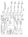
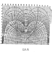
- the stability of the system is indicated by the Nichols' Chart shown in Figure 10 which shows an overall gain margin of about 20db and a phase margin of 70°. The linearity and control stability margins of the system are, therefore, very good.
- a feature of the present invention is to increase the frequency during the rise time interval so as to achieve a faster rise time with less current limiting and to thereby obtain a waveform that is very close to a square wave.
- Another aspect of the current level interaction phenomenon explained above is that, during the rise time, the mixing amplifier 129 is in saturation and, during that saturation interval, some type of control has to be applied to ensure that the system will recover rapidly from transformer core saturation and that control is maintained during that time interval.
- this control is established by inserting the output limiting circuit 135 on the feedback of the mixing amplifier 129 which prevents the error signal from going to extreme positions where it could be a long time before the capacitor 132 recovers to allow the error signal to be within the sawtooth generator intersectional limits to thereby quickly remove the mixer amplifier from saturation in order to achieve a good control at the end of such rise time interval.
- the Antisaturation Circuit 47 has to be matched to make sure the transformer 28 gets out of saturation because the dynamic asymmetry of the mark/space ratio or volts per second areas are applied to the inverter 27 and transformer 28 during such rise time.
- variable increasing mark/space ratio during the rise time can be accomplished by controlling the voltage demand slope by way of the microprocessor 30 through the D/A converter 52 to ensure that the small pulses at the beginning of the rise time will, in conjunction with the current limit on the power inverter, limit the current and also control the rise time interval.
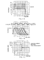
- FIGURES 11a-11f illustrate the performance of the present system when operating within various parameters with an MX-100 X-ray tube manufactured by General Electric Company.
- FIGURE lla shows a typical exposure time of 32 millisec. with a current load of 640 mA for different kilovolt levels of 55, 60, 70, 80, 90, and 100 kilovolts. It will be seen that, first of all, the rise time is very fast, i.e., within 1 millisec. Secondly, there is a very high linearity during the rise time and the overshoot is tightly controlled at the end of the rise time because of the phase advance coapensation. During the steady-state operation, the output ripple is seen to decrease with the output voltage so that the mrk/space ratio increases with increases in the voltage. However, the ripple is minimal in each case.
- FIGURE 11b shows exposure times of 1 millisecond and upward, when operating at voltage and current levels of 125 kV and 400 mA, respectively.
- the flat top on the kilovolts waveform demonstrates that the feedback operates in less than 1 millisec.
- This figure also shows, during the rise time period, several indications of where the current limit function operates to control the storing of energy on the filter capacitor and transformer during the rise time interval to thereby prevent an overshoot.
- the operational parameters are typical for X-ray generators working with automatic exposure control at very low mAs, where the reproducibility in conventional generators is very difficult to achieve due to the wide variation in load.
- the present invention achieves good performance under such conditions by controlling the kilovolts in a very fast closed-loop operation which assures no overshoot, a flat top, and a fast response.
- FIGURE llc shows an exposure at 110 kilovolts, 400 mA, and shows the current waveform on the inverter.
- the first interval during the non-linear rise time period, shows the current which is allowed to flow at a level higher than the steady-state level to achieve a fast rise time. It further shows a very symmetrical wave form both during the rise time and during the steady-state operation. This is indicative that, because of the operation of the Antisaturation Circuit 47, there is no saturation phenomenon in the transformer.
- This figure also shows that the transition between the rise time interval and the steady-state condition is done smoothly and fast, at the end of the phase advance operation and at the top reaching of the kilovolts.
- FIGURE lld shows a 200 mA, 7S kilovolts waveform with a 15 kilovolts step superimposed.
- FIGURE lld shows a 200 mA, 7S kilovolts waveform with a 15 kilovolts step superimposed.
- the settling time is very fast (on the order of less than 1 millisec).
- FIGURE lle shows the sane waveform but at a higher frequency and superimposed with a 7.5 kVp step to show the kilovolts frequency response.
- the bottom waveform is the clock generator which produces the variable transitional demand.
- FIGURE llf is similar to FIG. lie, at 75 kYp with 7.5 kVp superimposed, but the time scale is different and the frequency is now 5.5 kilohertz.
- the conclusions that can be drawn regardi.ng the voltage feedback controller are as follows: (1) there is substantially no overshoot over the wide range of techniques employed in the X-ray generator; (2) there is very good tracking at least up to 5.5 kilohertz; (3) there are no unstabilities but, rather, very good linearity and reproducibility; and (4) the behavior is that of a first order system (1/1 + ST).
Landscapes
- Health & Medical Sciences (AREA)
- General Health & Medical Sciences (AREA)
- Toxicology (AREA)
- X-Ray Techniques (AREA)
Applications Claiming Priority (2)
| Application Number | Priority Date | Filing Date | Title |
|---|---|---|---|
| US56453883A | 1983-12-22 | 1983-12-22 | |
| US564538 | 1983-12-22 |
Publications (2)
| Publication Number | Publication Date |
|---|---|
| EP0146875A2 true EP0146875A2 (de) | 1985-07-03 |
| EP0146875A3 EP0146875A3 (de) | 1987-08-05 |
Family
ID=24254882
Family Applications (1)
| Application Number | Title | Priority Date | Filing Date |
|---|---|---|---|
| EP84115236A Withdrawn EP0146875A3 (de) | 1983-12-22 | 1984-12-12 | Röntgenstrahlgenerator mit Spannungsregelkreis |
Country Status (4)
| Country | Link |
|---|---|
| EP (1) | EP0146875A3 (de) |
| JP (1) | JPS60221998A (de) |
| ES (1) | ES8707644A1 (de) |
| IL (1) | IL73556A0 (de) |
Cited By (5)
| Publication number | Priority date | Publication date | Assignee | Title |
|---|---|---|---|---|
| US4670893A (en) * | 1984-01-12 | 1987-06-02 | Kabushiki Kaisha Toshiba | X-ray diagnostic apparatus |
| US4789998A (en) * | 1986-03-27 | 1988-12-06 | Siemens Aktiengesellschaft | Medium frequency x-ray diagnostics generator power control |
| CN104582229A (zh) * | 2013-10-25 | 2015-04-29 | 南京普爱射线影像设备有限公司 | 一种用于x射线机灯丝系统的保护电路 |
| CN112149044A (zh) * | 2020-11-26 | 2020-12-29 | 海辉医学(北京)科技有限公司 | 一种x透视摄影中ma校准方法、装置、设备及存储介质 |
| CN113067553A (zh) * | 2021-03-17 | 2021-07-02 | 中国科学院近代物理研究所 | 反馈型脉冲线性放大的电子冷却调制方法及装置 |
Families Citing this family (1)
| Publication number | Priority date | Publication date | Assignee | Title |
|---|---|---|---|---|
| CN116156721B (zh) * | 2023-02-23 | 2023-12-12 | 无锡日联科技股份有限公司 | 一种采用双极性低纹波高精度可控恒流源电路的x射线源 |
Family Cites Families (8)
| Publication number | Priority date | Publication date | Assignee | Title |
|---|---|---|---|---|
| CA1120600A (en) * | 1977-09-23 | 1982-03-23 | Heikki K.J. Kanerva | Procedure for regulating and stabilizing the intensity level of the radiation of an x-ray source and an x-ray source where this procedure is used |
| US4167670A (en) * | 1978-02-03 | 1979-09-11 | General Electric Company | Dental X-ray apparatus |
| JPS5635399A (en) * | 1979-08-31 | 1981-04-08 | Hitachi Ltd | Power source device |
| JPS5753100A (en) * | 1980-09-13 | 1982-03-29 | Toshiba Corp | X-ray equipment |
| FR2507842A1 (fr) * | 1981-06-12 | 1982-12-17 | Gen Equip Med Sa | Regulateur de tension a semi-conducteur et generateur de radiologie comportant un tel regulateur |
| JPS5828200A (ja) * | 1981-08-13 | 1983-02-19 | Toshiba Corp | X線装置 |
| JPS58141599U (ja) * | 1982-03-18 | 1983-09-24 | 株式会社 モリタ製作所 | 医療用x線照射電源装置 |
| JPS58216397A (ja) * | 1982-06-11 | 1983-12-16 | Toshiba Corp | X線診断装置 |
-
1984
- 1984-11-20 IL IL73556A patent/IL73556A0/xx unknown
- 1984-12-12 EP EP84115236A patent/EP0146875A3/de not_active Withdrawn
- 1984-12-19 ES ES538808A patent/ES8707644A1/es not_active Expired
- 1984-12-21 JP JP59268737A patent/JPS60221998A/ja active Pending
Cited By (6)
| Publication number | Priority date | Publication date | Assignee | Title |
|---|---|---|---|---|
| US4670893A (en) * | 1984-01-12 | 1987-06-02 | Kabushiki Kaisha Toshiba | X-ray diagnostic apparatus |
| US4789998A (en) * | 1986-03-27 | 1988-12-06 | Siemens Aktiengesellschaft | Medium frequency x-ray diagnostics generator power control |
| CN104582229A (zh) * | 2013-10-25 | 2015-04-29 | 南京普爱射线影像设备有限公司 | 一种用于x射线机灯丝系统的保护电路 |
| CN112149044A (zh) * | 2020-11-26 | 2020-12-29 | 海辉医学(北京)科技有限公司 | 一种x透视摄影中ma校准方法、装置、设备及存储介质 |
| CN112149044B (zh) * | 2020-11-26 | 2021-03-05 | 海辉医学(北京)科技有限公司 | 一种x透视摄影中ma校准方法、装置、设备及存储介质 |
| CN113067553A (zh) * | 2021-03-17 | 2021-07-02 | 中国科学院近代物理研究所 | 反馈型脉冲线性放大的电子冷却调制方法及装置 |
Also Published As
| Publication number | Publication date |
|---|---|
| ES8707644A1 (es) | 1986-06-01 |
| ES538808A0 (es) | 1986-06-01 |
| JPS60221998A (ja) | 1985-11-06 |
| IL73556A0 (en) | 1985-02-28 |
| EP0146875A3 (de) | 1987-08-05 |
Similar Documents
| Publication | Publication Date | Title |
|---|---|---|
| US4654770A (en) | Current-limit circuit in X-ray generator | |
| US4601051A (en) | Protective circuit for X-ray generator | |
| US4596029A (en) | X-ray generator with phase-advance voltage feedback | |
| EP0087640B1 (de) | Steuereinrichtung für einen Umformer | |
| EP0146876A2 (de) | Antisättigungssteuereinrichtung für Röntgengenerator | |
| EP0146875A2 (de) | Röntgenstrahlgenerator mit Spannungsregelkreis | |
| JPH11206120A (ja) | パワーコンバータを制御するための方法及び装置 | |
| JPH0442908B2 (de) | ||
| EP0078252B1 (de) | Elektronisches Schweissgerät | |
| US4171488A (en) | X-ray diagnosis generator comprising an inverter feeding the high voltage transformer | |
| US10398011B2 (en) | Method and apparatus for active filament management | |
| US4439869A (en) | X-Ray generator for an X-ray tube comprising a grounded grid | |
| EP0146877A2 (de) | Hochspannungsspeiseanordnung für Röntgenstrahlgenerator | |
| JPS6338942B2 (de) | ||
| JPH0575999U (ja) | レントゲン線発生器 | |
| DE1943840C3 (de) | Vorrichtung zum Verbinden zweier Wechselstromnetze | |
| JPS6216066A (ja) | 電力変換装置の出力垂下方法 | |
| DE1139911B (de) | Steuereinrichtung fuer Mehrphasensynchrongeneratoren | |
| JPS5832399A (ja) | X線発生器の閉回路強度の静的制御方式 | |
| DE3322278A1 (de) | Schaltungsanordnung zur regelung der ausgangsspannung eines stromversorgungsgeraetes | |
| DE4120611C2 (de) | Verfahren zur Begrenzung der Zwischenkreisspannung eines Spannungszwischenkreis-Umrichters | |
| DE4010681C2 (de) | ||
| SU748721A1 (ru) | Стабилизированный конвертор | |
| DE3039282A1 (de) | Einrichtung zur nullstromerfassung bei umkehrstromrichtern | |
| DE2943794A1 (de) | Roentgendiagnostikanlage mit einer tastschaltung fuer die einstellung des roentgenroehrenstromes |
Legal Events
| Date | Code | Title | Description |
|---|---|---|---|
| PUAI | Public reference made under article 153(3) epc to a published international application that has entered the european phase |
Free format text: ORIGINAL CODE: 0009012 |
|
| AK | Designated contracting states |
Designated state(s): DE FR GB NL |
|
| PUAL | Search report despatched |
Free format text: ORIGINAL CODE: 0009013 |
|
| AK | Designated contracting states |
Kind code of ref document: A3 Designated state(s): DE FR GB NL |
|
| STAA | Information on the status of an ep patent application or granted ep patent |
Free format text: STATUS: THE APPLICATION IS DEEMED TO BE WITHDRAWN |
|
| 18D | Application deemed to be withdrawn |
Effective date: 19870101 |
|
| RIN1 | Information on inventor provided before grant (corrected) |
Inventor name: CARMENA, ANGEL DIAZ Inventor name: SANTURTUN, CARLOS MANUECO |