EP0145520B1 - Ecran d'affichage à matrice active sans croisement des lignes et des colonnes d'adressage - Google Patents
Ecran d'affichage à matrice active sans croisement des lignes et des colonnes d'adressage Download PDFInfo
- Publication number
- EP0145520B1 EP0145520B1 EP84401967A EP84401967A EP0145520B1 EP 0145520 B1 EP0145520 B1 EP 0145520B1 EP 84401967 A EP84401967 A EP 84401967A EP 84401967 A EP84401967 A EP 84401967A EP 0145520 B1 EP0145520 B1 EP 0145520B1
- Authority
- EP
- European Patent Office
- Prior art keywords
- row
- column
- conductors
- display screen
- image points
- Prior art date
- Legal status (The legal status is an assumption and is not a legal conclusion. Google has not performed a legal analysis and makes no representation as to the accuracy of the status listed.)
- Expired
Links
Images
Classifications
-
- G—PHYSICS
- G02—OPTICS
- G02F—OPTICAL DEVICES OR ARRANGEMENTS FOR THE CONTROL OF LIGHT BY MODIFICATION OF THE OPTICAL PROPERTIES OF THE MEDIA OF THE ELEMENTS INVOLVED THEREIN; NON-LINEAR OPTICS; FREQUENCY-CHANGING OF LIGHT; OPTICAL LOGIC ELEMENTS; OPTICAL ANALOGUE/DIGITAL CONVERTERS
- G02F1/00—Devices or arrangements for the control of the intensity, colour, phase, polarisation or direction of light arriving from an independent light source, e.g. switching, gating or modulating; Non-linear optics
- G02F1/01—Devices or arrangements for the control of the intensity, colour, phase, polarisation or direction of light arriving from an independent light source, e.g. switching, gating or modulating; Non-linear optics for the control of the intensity, phase, polarisation or colour
- G02F1/13—Devices or arrangements for the control of the intensity, colour, phase, polarisation or direction of light arriving from an independent light source, e.g. switching, gating or modulating; Non-linear optics for the control of the intensity, phase, polarisation or colour based on liquid crystals, e.g. single liquid crystal display cells
- G02F1/133—Constructional arrangements; Operation of liquid crystal cells; Circuit arrangements
- G02F1/136—Liquid crystal cells structurally associated with a semi-conducting layer or substrate, e.g. cells forming part of an integrated circuit
- G02F1/1362—Active matrix addressed cells
- G02F1/1368—Active matrix addressed cells in which the switching element is a three-electrode device
-
- G—PHYSICS
- G02—OPTICS
- G02F—OPTICAL DEVICES OR ARRANGEMENTS FOR THE CONTROL OF LIGHT BY MODIFICATION OF THE OPTICAL PROPERTIES OF THE MEDIA OF THE ELEMENTS INVOLVED THEREIN; NON-LINEAR OPTICS; FREQUENCY-CHANGING OF LIGHT; OPTICAL LOGIC ELEMENTS; OPTICAL ANALOGUE/DIGITAL CONVERTERS
- G02F1/00—Devices or arrangements for the control of the intensity, colour, phase, polarisation or direction of light arriving from an independent light source, e.g. switching, gating or modulating; Non-linear optics
- G02F1/01—Devices or arrangements for the control of the intensity, colour, phase, polarisation or direction of light arriving from an independent light source, e.g. switching, gating or modulating; Non-linear optics for the control of the intensity, phase, polarisation or colour
- G02F1/13—Devices or arrangements for the control of the intensity, colour, phase, polarisation or direction of light arriving from an independent light source, e.g. switching, gating or modulating; Non-linear optics for the control of the intensity, phase, polarisation or colour based on liquid crystals, e.g. single liquid crystal display cells
- G02F1/133—Constructional arrangements; Operation of liquid crystal cells; Circuit arrangements
- G02F1/136—Liquid crystal cells structurally associated with a semi-conducting layer or substrate, e.g. cells forming part of an integrated circuit
- G02F1/1362—Active matrix addressed cells
-
- G—PHYSICS
- G09—EDUCATION; CRYPTOGRAPHY; DISPLAY; ADVERTISING; SEALS
- G09G—ARRANGEMENTS OR CIRCUITS FOR CONTROL OF INDICATING DEVICES USING STATIC MEANS TO PRESENT VARIABLE INFORMATION
- G09G3/00—Control arrangements or circuits, of interest only in connection with visual indicators other than cathode-ray tubes
- G09G3/20—Control arrangements or circuits, of interest only in connection with visual indicators other than cathode-ray tubes for presentation of an assembly of a number of characters, e.g. a page, by composing the assembly by combination of individual elements arranged in a matrix no fixed position being assigned to or needed to be assigned to the individual characters or partial characters
- G09G3/34—Control arrangements or circuits, of interest only in connection with visual indicators other than cathode-ray tubes for presentation of an assembly of a number of characters, e.g. a page, by composing the assembly by combination of individual elements arranged in a matrix no fixed position being assigned to or needed to be assigned to the individual characters or partial characters by control of light from an independent source
- G09G3/36—Control arrangements or circuits, of interest only in connection with visual indicators other than cathode-ray tubes for presentation of an assembly of a number of characters, e.g. a page, by composing the assembly by combination of individual elements arranged in a matrix no fixed position being assigned to or needed to be assigned to the individual characters or partial characters by control of light from an independent source using liquid crystals
- G09G3/3611—Control of matrices with row and column drivers
- G09G3/3648—Control of matrices with row and column drivers using an active matrix
- G09G3/3655—Details of drivers for counter electrodes, e.g. common electrodes for pixel capacitors or supplementary storage capacitors
-
- G—PHYSICS
- G02—OPTICS
- G02F—OPTICAL DEVICES OR ARRANGEMENTS FOR THE CONTROL OF LIGHT BY MODIFICATION OF THE OPTICAL PROPERTIES OF THE MEDIA OF THE ELEMENTS INVOLVED THEREIN; NON-LINEAR OPTICS; FREQUENCY-CHANGING OF LIGHT; OPTICAL LOGIC ELEMENTS; OPTICAL ANALOGUE/DIGITAL CONVERTERS
- G02F2201/00—Constructional arrangements not provided for in groups G02F1/00 - G02F7/00
- G02F2201/12—Constructional arrangements not provided for in groups G02F1/00 - G02F7/00 electrode
- G02F2201/122—Constructional arrangements not provided for in groups G02F1/00 - G02F7/00 electrode having a particular pattern
-
- G—PHYSICS
- G09—EDUCATION; CRYPTOGRAPHY; DISPLAY; ADVERTISING; SEALS
- G09G—ARRANGEMENTS OR CIRCUITS FOR CONTROL OF INDICATING DEVICES USING STATIC MEANS TO PRESENT VARIABLE INFORMATION
- G09G3/00—Control arrangements or circuits, of interest only in connection with visual indicators other than cathode-ray tubes
- G09G3/20—Control arrangements or circuits, of interest only in connection with visual indicators other than cathode-ray tubes for presentation of an assembly of a number of characters, e.g. a page, by composing the assembly by combination of individual elements arranged in a matrix no fixed position being assigned to or needed to be assigned to the individual characters or partial characters
- G09G3/2007—Display of intermediate tones
- G09G3/2011—Display of intermediate tones by amplitude modulation
Definitions
- the present invention relates to an active matrix display screen without crossing the row and column addressing conductors. It finds an application in optoelectronics in the production of liquid crystal displays used in particular as converters of electrical information into optical information.
- a known type of solution consists in incorporating the electrical threshold and the memory effect at each image point.
- This threshold can be ensured by a thin film transistor, by a varistor or by a MIM (metal-insulator-metal) switch, or the like.
- MIM metal-insulator-metal
- each image point is therefore located at the intersection of a line and a connection column and it consists of a transistor, for example, and a capacitor.
- the armatures of the capacitor can be formed by the electrodes of the liquid crystal cell itself.
- the image point is therefore reduced to a transistor and to a capacitor, one of the armatures of which is formed by the electrode placed on the wall of the cell which contains the transistor, the other armature being constituted of the counter-electrode. arranged on the other wall of the cell.
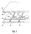
- FIG. 1 Such a structure is shown in FIG. 1.
- a lower wall 10 carrying conductive columns 12 and conductive lines 14, a thin film transistor 20 and a transparent electrode 22, and on the other hand, an upper wall 24 covered with a counter-electrode 26 also transparent.
- the structure described in application EP-A-070 598 comprises two support plates between which an optoelectronic transducer is placed.
- a structure which moreover comprises switching elements produced from head-to-tail diodes, does not make it possible to obtain an active matrix architecture in which the switching elements are transistors and in which the line and column crossovers of the display screen.
- the invention provides an active de-matrix architecture eliminating these crossings of row and column conductors.
- the invention replaces the counter-electrode on the upper face with a family of column electrodes.
- the underside no longer supports the conductive columns.
- the crossings of conductive rows and columns being eliminated, the short-circuits are eliminated and the production efficiency of such an active matrix is significantly increased.
- the first wall contains all the slow logic produced for example in hydrogenated Si and the second wall contains all the fast logic produced for example in polycrystalline Si whereas in the prior art these two technologies are produced on the same substrate .
- the subject of the invention is therefore an active matrix display screen comprising a material whose optical characteristic can be modified, this material being interposed between a first wall and a second transparent wall, said screen comprising a plurality of image points arranged in a matrix of pxq elements, where 1 ⁇ p and 1 ⁇ q, a first family of p addressing conductors of a row of image points, a second family of q addressing conductors of a column of picture points, each image point consisting of a switching element and a capacitor formed by two electrodes each disposed on one of the two walls, the first wall of said screen carrying a matrix of elements each consisting of the switching element and of an electrode and carrying the first family of p row conductors and the second transparent wall carrying a family of q column electrodes and the second family of q column conductors, the electrodes and conductors of the same rank being interconnected, said screen being characterized in that the switching element of each image point is a thin film transistor whose gate is connected to a line conductor
- each line of image points is associated with a line conductor disposed on one side of said line of image points and parallel to it, and a conductor brought to the constant potential and arranged parallel to said line of image points, on the other side thereof.
- the average value of the signal applied to each column electrode is constant over the period of a frame.
- the width Tc of the slot of the signal applied to each column electrode during the time TL for addressing a line is equal to ⁇ L / 2.
- the line addressing signal contains, during each frame, a single slot of width TL / 2.
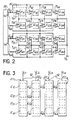
- FIG. 2 shows the elements of the active matrix produced on one of the paroids of a display screen according to the invention.
- This screen includes 16 image points arranged in a 4x4 matrix.
- Each element 30 constitutes a part of an image point.
- Each of these elements consists of a thin film transistor denoted T and an electrode denoted E. These transistor and electrode are conventionally represented by subscript figures indicating their row and column number in the matrix.
- V Gi The potential applied on the ith line, where 1 ⁇ i ⁇ 4, is noted V Gi .
- This line potential is delivered by a shift register 32 which delivers a voltage slot successively on each of the line conductors 14.
- each transistor in the matrix is connected to a constant potential V s .
- This potential acts as a charge source for each of the electrodes of the elements 30 whose transistor is activated by a voltage pulse on its gate.
- FIG. 3 represents the part of the active matrix of a display screen produced on the other wall of this screen.
- 4 column electrodes EC, EC 2 , EC 3 , EC 4 were produced .
- Each of these electrodes is connected to a column conductor 12.
- each display point of an image point therefore consists of the area where an electrode of one wall and an electrode of the other wall are superimposed. These display points are in fact geometrically coincident with the electrodes of the first wall.
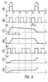
- FIG. 4a represents the voltage V G1 applied to the gate of the transistors of the first line, that is to say on the transistors T 11 , T, 2 , T 13 and T 14 .
- the time axis is divided into intervals of constant length.
- the time interval between the dates 0 and t 4 corresponds to a frame, that is to say to the addressing time of all the image points.
- the length ⁇ L is equal to the duration of the addressing of a line of the screen. Each point of the line is in fact only activated during the time interval T , during which the line voltage V G1 is not zero.
- this time interval T is at least equal to half the time interval TL for addressing the line.
- FIG. 4b represents the voltage V C1 applied to the electrode EC, (FIG. 3) as a function of the time.
- This potential V C1 or more exactly the difference between the potential V C1 , and the constant source potential V S determines, when the first line of transistor is addressed, the charge of the image point located at the intersection of the first line and the first column.
- the signal V C1 consists of a slot of width- ⁇ c in each time interval TL .
- the slots in dashed lines correspond to the addressing of the image points located at the intersection of the first column and, respectively, of the second, third and fourth lines.
- the position of the slot of the signal V C1 , in the interval ⁇ L determines the gray level of the image point.
- FIG. 4c shows the charge Q 11 of the capacitor constituting the display point located at the intersection of the first line and the first column.
- the signal V G1 does not exhibit a voltage pulse.
- the charge Q 11 is therefore retained.
- the charge of the capacitor is modified.
- the column signal V C1 then being zero at this instant, the capacitor discharges.
- FIG. 4d The optical aspect related to the capacitive effect shown in Figure 4c is illustrated in Figure 4d.
- the curve in this figure represents the gray level of the image point. At the initial instant, the point is black, then when the capacity charges the image point becomes white. It becomes black again when the capacity discharges between instants t 4 and t s .
- Figures 4d, 4e and 4f represent, for the image point located at the intersection of the first line and the second column, respectively the same curves as those represented in 4b, 4c and 4d for the image point located at the intersection of the first row and the first column.
- the voltage pulse of signal V c2 applied to the second column electrode between times 0 and t 1 partially covers the voltage pulse applied during this same instant to signal V G1 . This results in a partial charge on the Q 12 Consensor of the image point. This charge is not altered, apart from capacity leaks, until a new voltage window appears on the signal V G1 . This occurs between instants t 4 and t s . The voltage slot appearing in this time interval on the column signal V C2 completely covers the voltage slot of the signal V G1 . The image point capacitor therefore charges fully.
- the image point changes from black to a gray level between the instants of start and end of the voltage slot on the signal V G1 . It then passes from this gray level to the white level between the instants of start and end of the consecutive voltage pulse of the signal V G1 .
Landscapes
- Physics & Mathematics (AREA)
- Engineering & Computer Science (AREA)
- Chemical & Material Sciences (AREA)
- Crystallography & Structural Chemistry (AREA)
- Nonlinear Science (AREA)
- General Physics & Mathematics (AREA)
- Mathematical Physics (AREA)
- Microelectronics & Electronic Packaging (AREA)
- Theoretical Computer Science (AREA)
- Computer Hardware Design (AREA)
- Optics & Photonics (AREA)
- Power Engineering (AREA)
- Liquid Crystal (AREA)
- Devices For Indicating Variable Information By Combining Individual Elements (AREA)
- Liquid Crystal Display Device Control (AREA)
- Control Of Indicators Other Than Cathode Ray Tubes (AREA)
Description
- La présente invention a pour objet un écran d'affichage à matrice active sans croisement des conducteurs d'adressage lignes et colonnes. Elle trouve une application en optoélectronique dans la réalisation d'afficheurs à cristaux liquides utilisés notamment comme convertisseurs d'information électriques en informations optiques.
- La plupart des écrans d'afficharge à cristaux liquides d'une complexité égale ou supérieure à 105 points élémentaires d'image utilisent un adressage matriciel. Ce mode d'adressage possède des limitations propres qui sont en particulier étudiées dans l'article "Perspective actuelle de présentation d'images sur panneaux plats" paru dans la revue "OPTO" no 6, septembre 1981, pages 29 à 31. Ces limitations concernent principalement, d'une part, la sélectivité d'adressage d'un point élémentaire d'image et d'autre part, la vitesse d'affichage.
- Pour sélectionner un point d'image particulier, il faut en effet que la différence de potentiel entre la ligne et la colonne à l'intersection desquelles se trouve ledit point d'image soit supérieure à une tension de seuil Vs et que simulanément la tension en chacun des autres points d'image soit notablement inférieure à cette même tension de seuil VS. Ceci est généralement réalisé en appliquant des tensions non nulles et judicieusement choisies sur les lignes et les colonnes non sélectionnées. Il en résulte une dépense énergétique importante qui croît linéairement avec le nombre de lignes.
- Par ailleurs, plus le nombre de lignes d'affichage est important, plus la vitesse d'inscription est élevée. L'intervalle de temps séparant l'inscription de deux lignes successives est donc faible et la puissance moyenne nécessaire croît. Il y a donc un comprimis entre la dimension de l'écran, la puissance disponible et la rapidité d'adressage.
- Pour dépasser les limitations de l'adressage matriciel, un type de solution connu consiste à incorporer le seuil électrique et l'effet mémoire au niveau de chaque point d'image. Ce seuil peut être assuré par un transistor en couche mince, par un varistor ou par un commutateur MIM (métal- isolant-métal), ou autre. Une telle structure est dite à matrice active.
- Dans une matrice active, chaque point d'image est donc situé au croisement d'une ligne et d'une colonne de connexion et il est constitué d'un transistor, par exemple, et d'un condensateur.
- Dans le cas où le transducteur optoélectronique est un cristal liquide, les armatures du condensateur peuvent être constituées par les électrodes de la cellule à cristal liquide elle-même. Le point d'image se ramène donc à un transistor et à un condensateur dont l'une des armatures est constituée par l'électrode disposée sur la paroi de la cellule qui contient le transistor, l'autre armature étant constituée par la contre-électrode disposée sur l'autre paroi de la cellule.
- Une telle structure est représentée sur la figure 1. On y voit, d'une part, une paroi inférieure 10 portant des colonnes conductrices 12 et des lignes conductrices 14, un transistor en couche mince 20 et une électrode transparente 22, et d'autre part, une paroi supérieure 24 recouverte d'une contre-électrode 26 également transparente.
- A chaque croisement 28 de conducteurs, lignes et colonnes, il faut évidemment assurer l'isolement électrique desdits conducteurs. Ceci constitue précisément l'un des problèmes technologiques mal résolus à ce jour. En effet, de nombreux courts-circuits se produisent sur ces croisements rendant le plus souvent inutilisable la matrice active et faisant chuter d'autant les rendements de fabrication.
- Des structure d'écran d'affichage ont été décrites, on pourra se référer à la demande de brevet européen EP-A-0 034 796 et plus particulièrement à la demande EP-A-070 598 dans lesquelles une structure d'affichage a été décrite.
- La structure décrite dans la demande EP-A-070 598 comprend deux plaques support entre lesquelles un transducteur optoélectronique est placé. Cependant une telle structure, qui comporte d'ailleurs des éléments de commutation réalisés à partir de diodes tête-bêche, ne permet pas d'obtenir une architecture de matrice active dans laquelle les éléments de commutation sont des transistors et dans laquelle on a supprimé les croisements des conducteurs ligne et colonne de l'écran d'affichage.
- Pour remédier à ces inconvénients, l'invention propose une architecture de-matrice active supprimant ces croisements de conducteurs lignes et colonnes.
- Plus précisément, l'invention remplace sur la face supérieure la contre-électrode par une famille d'électrodes colonnes. La face inférieure ne supporte plus les colonnes conductrices. Les croisements de lignes et colonnes conductrices étant supprimés, les courts-circuits sont éliminés et le rendement de fabrication d'une telle matrice active est augmenté de façon notable.
- Un autre avantage de l'invention réside dans la simplification de la fabrication d'un écran d'affichage. En effet, la première paroi contient toute la logique lente réalisée par exemple en Si hydrogéné et la deuxième paroi contient toute la logique rapide réalisée par exemple en Si polycrystal- lin alors que dans l'art antérieur ces deux technologies sont réalisées sur le même substrat.
- Enfin, on peut noter que le test de contrôle d'une ligne de point d'image est très simple.
- L'invention a donc pour objet un écran d'affichage à matrice active comprenant un matériau dont on peut modifier la caractéristique optique, ce matériau étant intercalé entre une première paroi et une seconde paroi transparente, ledit écran comportant une pluralité de points d'image disposés en une matrice de pxq éléments, où 1<p et 1<q, une première famille de p conducteurs d'adressage d'une ligne de points d'image, une deuxième famille de q conducteurs d'adressage d'une colonne de points d'image, chaque point d'image étant constitué d'un élément de commutation et d'un condensateur formé de deux électrodes disposées chacune sur l'une des deux parois, la première paroi dudit écran portant une matrice d'éléments constitués chacun de l'élément de commutation et d'une électrode et portant la première famille de p conducteurs lignes et la deuxième paroi transparente portant une famille de q électrodes colonnes et la deuxième famille de q conducteurs colonnes, les électrodes et conducteurs de même rang étant reliés entre eux, ledit écran étant caractérisé en ce que l'élément de commutation de chaque point d'image est un transistor en couche mince dont la grille est reliée à un conducteur ligne, la source à un potentiel de référence constant (VS) et le drain à l'électrode associée audit transistor faisant partie d'un élément de la matrice portée par la première paroi et en ce que à chaque ligne de points d'image sont associés un conducteur ligne disposé d'un côté de ladite ligne de points d'image et parallèlement à celle-ci et un conducteur porté au potentiel constant (Vs) et disposé parallèlement à ladite ligne de points d'image, de l'autre côté de celle-ci.
- Selon une caractéristique de l'écran de l'invention, à chaque ligne de points d'image sont associés un conducteur ligne disposé d'un côté de ladite ligne de points d'image et parallèlement à celle-ci, et un conducteur porté au potentiel constant et disposé parallèlement à ladite ligne de points d'image, de l'autre côté de celle-ci.
- Selon une caractéristique secondaire, la valeur moyenne du signal appliqué sur chaque électrode colonne est constante sur la période d'une trame.
- Selon une autre caractéristique secondaire, la largeur Tc du créneau du signal appliqué sur chaque électrode colonne pendant le temps TL d'adressage d'une ligne est égale à τL/2.
- Selon une autre caractéristique secondaire, le signal d'adressage ligne contient, pendant chaque trame, un créneau unique et de largeur TL/2.
- D'autres caractéristiques et avantages de l'invention ressortiront mieux de la description qui va suivre, donnée à titre purement illustratif et nullement limitatif, en référence aux figures annexées, dans lesquelles:
- la figure 1, déjà décrite, illustre un mode de réalisation connu d'un écran d'affichage à matrice active,
- la figure 2 représente, schématiquement, la matrice de transistors et d'électrodes ainsi que les conducteurs lignes réalisés sur l'une des parois de la cellule,
- la figure 3 représente, schématiquement, les électrodes colonnes et les conducteurs colonnes réalisés sur l'autre paroi de la cellule,
- la figure 4 est un chronogramme illustrant la commande d'un point d'image.
- On a représenté sur la figure 2 les éléments de la matrice active réalisés sur l'une des paroids d'un écran d'affichage conforme à l'invention. Cet écran comprend 16 points d'image disposés dans une matrice 4x4. Chaque élément 30 constitue une partie d'un point d'image. Chacune de ces éléments est constitué d'un transistor en couche mince noté T et d'une électrode notée E. Ces transistor et électrode sont reprérés classiquement par des chiffres en indice indiquant leur numéro de ligne et de colonne dans la matrice.
- Les grilles de tous les transistors d'une même ligne sont reliées entre elles. Le potentiel appliqué sur la ième ligne, où 1<i<4, est noté VGi. Ce potentiel ligne est délivré par un registre à décalage 32 qui délivre un créneau de tension successivement sur chacun des conducteurs lignes 14.
- La source de chaque transistor de la matrice est reliée à un potentiel constant Vs. Ce potentiel agit comme une source de charge pour chacune des électrodes des éléments 30 dont le transistor est activé par un créneau de tension sur sa grille.
- L'absence de croisement entre les conducteurs de lignes amenant les tensions VG1, VG2, VG3 et VG4 et les conducteurs amenant le potentiel constant Vs peut s'obtenir, comme représenté sur la figure 2, de la manière suivante. Tous ces conducteurs sont tracés parallèles entre eux et à une ligne de points d'image et les deux conducteurs associés à chaque ligne de points d'image sont disposés chacun d'un côté de cette ligne de points d'image.
- La figure 3 représente la partie de la matrice active d'un écran d'affichage réalisée sur l'autre paroi de cet écran. Sur cette paroi, ont été réalisées 4 électrodes colonnes EC,, EC2, EC3, EC4. Chacune de ces électrodes est reliée à un conducteur colonne 12.
- Pour une bonne compréhension de l'architecture de la matrice active selon l'invention, on a représenté en traits tiretés la matrice d'électrodes réalisée sur la première paroi. Chaque point d'affichage d'un point d'image est donc constitué par la zone où une électrode d'une paroi et une électrode de l'autre paroi sont superposées. Ces points d'affichage sont en fait géométriquement confondus avec les électrodes de la première paroi.
- Le fonctionnement de l'écran d'affichage de la matrice active décrit en référence aux figures 2 et 3, c'est-à-dire la manière de commander l'affichage d'un point quelconque de cet écran, va être expliqué à l'aide des chronogrammes des figures 4a à 4g.
- La figure 4a représente la tension VG1 appliquée sur la grille des transistors de la première ligne, c'est-à-dire sur les transistors T11, T,2, T13 et T14. L'axe des temps est divisé en intervalles de longeur constante. L'intervalle de temps compris entre les dates 0 et t4 correspond à une trame, c'est-à-dire au temps d'adressage de tous les points d'image.
- La longueur τL est égale à la durée de l'adressage d'une ligne de l'écran. Chaque point de la ligne n'est en fait activé que pendant l'intervalle de temps T, pendant lequel la tension de ligne VG1 n'est pas nulle.
- De manière préférée, cet intervalle de temps T, est au moins égal à la moitié de l'intervalle de temps TL d'adressage de la ligne.
- La figure 4b représente la tension VC1 appliquée sur l'électrode EC, (figure 3) en fonction du temps. Ce potentiel VC1, ou plus exactement la différence entre le potentiel VC1, et le potentiel source constant VS détermine, lorsque la première ligne de transistor est adressée, la charge du point d'image situé à l'intersection de la première ligne et de la première colonne.
- Le signal VC1, est constitué d'un créneau de largeur-τc dans chaque intervalle de temps TL. Les créneaux en traits tiretés correspondent à l'adressage des points d'image situés à l'intersection de la première colonne et, respectivement, des deuxième, troisième et quatrième lignes. La position du créneau du signal VC1, dans l'intervalle τL détermine le niveau de gris du point d'image.
- On a représenté sur la figure 4c la charge Q11 du condensateur constituant le point d'affichage situé à l'intersection de la première ligne et de la première colonne. Pendant l'intervalle de temps s'écoulant entre les dates 0 et t,, le signal VG1 présente un créneau de tension, les points d'image de la première ligne sont donc adressés. Pendant ce créneau, le signal VC1 présente également un créneau de tension. Le condensateur se charge donc.
- Pendant l'intervalle de temps s'écoulant entre les dates t1 à t4, le signal VG1 ne présente pas de créneau de tension. La charge Q11 est donc conservée. Lorsqu'apparaît un créneau de tension sur le signal VG1, la charge du condensateur est modifiée. Le signal colonne VC1 étant alors nul à cet instant, le condensateur se décharge.
- L'aspect optique lié à l'effet capacitif représenté sur la figure 4c est illustré sur la figure 4d. La courbe de cette figure représente le niveau de gris du point d'image. A l'instant initial, le point est noir, puis lorsque la capacité se charge le point image devient blanc. Il redevient noir lorsque la capacité se décharge entre les instants t4 et ts.
- Les figures 4d, 4e et 4f représentent, pour le point d'image situé à l'intersection de la première ligne et de la deuxième colonne, respectivement les mêmes courbes que celles représentées en 4b, 4c et 4d pour le point d'image situé à l'intersection de la première ligne et de la première colonne.
- Le créneau de tension du signal Vc2 appliqué sur la deuxième électrode colonne entre les instants 0 et t1 recouvre partiellement le créneau de tension appliqué pendant ce même instant sur le signal VG1. Il en résulte une charge partielle sur le consensateur Q12 du point d'image. Cette charge n'est pas altérée, aux fuites de capacité près, jusqu'à ce qu'un nouveau créneau de tension apparaisse sur le signal VG1. Ceci se produit entre les instants t4 et ts. Le créneau de tension apparaissant dans cet intervalle de temps sur le signal colonne VC2 recouvre totalement le créneau de tension du signal VG1. Le condensateur du point d'image se charge donc complètement.
- Du point de vue optique (figure 4g), le point d'image passe du noir à un niveau de gris entre les instants de début et de fin du créneau de tension sur le signal VG1. Il passe ensuite de ce niveau de gris au niveau blanc entre les instants de début et de fin du créneau de tension consécutif du signal VG1.
Claims (4)
Applications Claiming Priority (2)
| Application Number | Priority Date | Filing Date | Title |
|---|---|---|---|
| FR8315996A FR2553218B1 (fr) | 1983-10-07 | 1983-10-07 | Ecran d'affichage a matrice active sans croisement des lignes et des colonnes d'adressage |
| FR8315996 | 1983-10-07 |
Publications (3)
| Publication Number | Publication Date |
|---|---|
| EP0145520A2 EP0145520A2 (fr) | 1985-06-19 |
| EP0145520A3 EP0145520A3 (en) | 1985-07-10 |
| EP0145520B1 true EP0145520B1 (fr) | 1989-01-04 |
Family
ID=9292929
Family Applications (1)
| Application Number | Title | Priority Date | Filing Date |
|---|---|---|---|
| EP84401967A Expired EP0145520B1 (fr) | 1983-10-07 | 1984-10-02 | Ecran d'affichage à matrice active sans croisement des lignes et des colonnes d'adressage |
Country Status (5)
| Country | Link |
|---|---|
| US (1) | US4694287A (fr) |
| EP (1) | EP0145520B1 (fr) |
| JP (1) | JPS60107690A (fr) |
| DE (1) | DE3475975D1 (fr) |
| FR (1) | FR2553218B1 (fr) |
Families Citing this family (27)
| Publication number | Priority date | Publication date | Assignee | Title |
|---|---|---|---|---|
| EP0182645B1 (fr) * | 1984-11-16 | 1991-01-23 | Matsushita Electric Industrial Co., Ltd. | Circuit de matrice active pour affichage à cristaux liquides |
| US4678282A (en) * | 1985-02-19 | 1987-07-07 | Ovonic Imaging Systems, Inc. | Active display matrix addressable without crossed lines on any one substrate and method of using the same |
| GB8508656D0 (en) * | 1985-04-03 | 1985-05-09 | Gen Electric Co Plc | Liquid crystal displays |
| JPS62108227A (ja) * | 1985-10-31 | 1987-05-19 | インタ−ナショナル ビジネス マシ−ンズ コ−ポレ−ション | デイスプレイ装置 |
| FR2590394B1 (fr) * | 1985-11-15 | 1987-12-18 | Thomson Csf | Ecran de visualisation electro-optique a transistors de commande |
| FR2593632B1 (fr) * | 1986-01-27 | 1988-03-18 | Maurice Francois | Ecran d'affichage a matrice active et procedes de realisation de cet ecran |
| EP0238867B1 (fr) * | 1986-02-21 | 1994-12-14 | Canon Kabushiki Kaisha | Dispositif d'affichage |
| KR900004989B1 (en) * | 1986-09-11 | 1990-07-16 | Fujitsu Ltd | Active matrix type display and driving method |
| FR2606194B1 (fr) * | 1986-11-05 | 1989-02-17 | Commissariat Energie Atomique | Dispositif d'affichage matriciel et procede de commande de ce dispositif |
| FR2614718B1 (fr) * | 1987-04-28 | 1989-06-16 | Commissariat Energie Atomique | Ecran matriciel d'affichage a cristaux liquides muni de capacites de stockage |
| FR2625827B1 (fr) * | 1988-01-11 | 1993-07-16 | Commissariat Energie Atomique | Ecran d'affichage en couleur a matrice active sans croisement des conducteurs lignes d'adressage et des conducteurs colonnes de commande |
| US4968119A (en) * | 1989-01-10 | 1990-11-06 | David Sarnoff Research Center, Inc. | High-density liquid-crystal active dot-matrix display structure |
| KR940005240B1 (ko) * | 1990-05-07 | 1994-06-15 | 후지스 가부시끼가이샤 | 고성능 엑티브 매트릭스(active matrix)형 표시장치 |
| EP0536964B1 (fr) * | 1991-10-05 | 1998-03-18 | Fujitsu Limited | Dispositif d'affichage à cristaux liquides à matrice active avec un nombre réduit de lignes de bus de données |
| US5493439A (en) * | 1992-09-29 | 1996-02-20 | Engle; Craig D. | Enhanced surface deformation light modulator |
| US5488505A (en) * | 1992-10-01 | 1996-01-30 | Engle; Craig D. | Enhanced electrostatic shutter mosaic modulator |
| US5561548A (en) * | 1992-10-07 | 1996-10-01 | Engle; Craig D. | Enhanced membrane light modulator |
| US5521746A (en) * | 1993-02-22 | 1996-05-28 | Engle; Craig D. | Poppet valve modulator |
| JP3300282B2 (ja) | 1998-04-30 | 2002-07-08 | シャープ株式会社 | 液晶表示装置および液晶表示装置の製造方法 |
| JP3519310B2 (ja) * | 1998-06-12 | 2004-04-12 | シャープ株式会社 | 液晶表示装置 |
| JP3699850B2 (ja) | 1999-01-29 | 2005-09-28 | シャープ株式会社 | 表示装置および液晶表示装置 |
| JP3658260B2 (ja) | 1999-04-30 | 2005-06-08 | シャープ株式会社 | 液晶表示装置 |
| JP3527168B2 (ja) | 1999-06-02 | 2004-05-17 | シャープ株式会社 | 液晶表示装置 |
| US7088330B2 (en) | 2000-12-25 | 2006-08-08 | Sharp Kabushiki Kaisha | Active matrix substrate, display device and method for driving the display device |
| JP2003216062A (ja) * | 2002-01-18 | 2003-07-30 | Sharp Corp | 表示装置 |
| WO2008007300A1 (fr) | 2006-07-11 | 2008-01-17 | Koninklijke Philips Electronics N.V. | Disposition améliorée d'électrodes pour affichage |
| JP5344776B2 (ja) * | 2010-03-10 | 2013-11-20 | シャープ株式会社 | 表示装置 |
Family Cites Families (11)
| Publication number | Priority date | Publication date | Assignee | Title |
|---|---|---|---|---|
| US4233602A (en) * | 1977-03-30 | 1980-11-11 | Hitachi, Ltd. | Multi-matrix display system having matrix display panel with uncrossed connections on substrates |
| US4110664A (en) * | 1977-04-15 | 1978-08-29 | Westinghouse Electric Corp. | Electroluminescent bargraph with integral thin-film transistor control circuitry |
| US4233603A (en) * | 1978-11-16 | 1980-11-11 | General Electric Company | Multiplexed varistor-controlled liquid crystal display |
| DE3071167D1 (en) * | 1979-08-03 | 1985-11-14 | Hughes Aircraft Co | Method and apparatus for multi-mode image display with a liquid crystal light valve |
| JPS5691277A (en) * | 1979-12-25 | 1981-07-24 | Citizen Watch Co Ltd | Liquiddcrystal display panel |
| EP0034796B1 (fr) * | 1980-02-22 | 1987-09-16 | Kabushiki Kaisha Toshiba | Dispositif d'affichage à cristaux liquides |
| JPS575083A (en) * | 1980-06-13 | 1982-01-11 | Tokyo Shibaura Electric Co | Display unit |
| FR2499744B1 (fr) * | 1981-01-05 | 1986-07-04 | Commissariat Energie Atomique | Dispositif d'affichage matriciel comprenant deux familles d'electrodes lignes et son procede de commande |
| JPS57201295A (en) * | 1981-06-04 | 1982-12-09 | Sony Corp | Two-dimensional address device |
| NL8103376A (nl) * | 1981-07-16 | 1983-02-16 | Philips Nv | Weergeefinrichting. |
| US4406997A (en) * | 1981-09-30 | 1983-09-27 | International Business Machines Corporation | Method and means for minimizing the effect of short circuits in flat panel displays |
-
1983
- 1983-10-07 FR FR8315996A patent/FR2553218B1/fr not_active Expired
-
1984
- 1984-10-02 EP EP84401967A patent/EP0145520B1/fr not_active Expired
- 1984-10-02 DE DE8484401967T patent/DE3475975D1/de not_active Expired
- 1984-10-05 JP JP59209605A patent/JPS60107690A/ja active Pending
- 1984-10-05 US US06/658,049 patent/US4694287A/en not_active Expired - Fee Related
Also Published As
| Publication number | Publication date |
|---|---|
| US4694287A (en) | 1987-09-15 |
| JPS60107690A (ja) | 1985-06-13 |
| EP0145520A2 (fr) | 1985-06-19 |
| FR2553218B1 (fr) | 1987-09-25 |
| EP0145520A3 (en) | 1985-07-10 |
| DE3475975D1 (en) | 1989-02-09 |
| FR2553218A1 (fr) | 1985-04-12 |
Similar Documents
| Publication | Publication Date | Title |
|---|---|---|
| EP0145520B1 (fr) | Ecran d'affichage à matrice active sans croisement des lignes et des colonnes d'adressage | |
| US4223308A (en) | LCDs (Liquid crystal displays) controlled by thin film diode switches | |
| FR2507803A1 (fr) | Dispositif d'affichage en matrice a cristaux liquides | |
| US4251136A (en) | LCDs (Liquid crystal displays) controlled by thin film diode switches | |
| FR2542119A1 (fr) | Procede pour commander un ecran d'affichage matriciel a cristaux liquides | |
| FR2488013A1 (fr) | Dispositif a matrice d'elements actifs | |
| EP0332476B1 (fr) | Ecran d'affichage en couleur à matrice active sans croisement des conducteurs lignes d'adressage et des conducteurs colonnes de commande | |
| EP2439583B1 (fr) | Afficheur a cristal liquide de type transmissif en technologie CMOS avec capacité de stockage auxiliaire | |
| FR2635902A1 (fr) | Procede de commande tres rapide par adressage semi-selectif et adressage selectif d'un panneau a plasma alternatif a entretien coplanaire | |
| FR2585167A1 (fr) | Structures conductrices redondantes pour affichages a cristaux liquides commandes par des transistors a effet de champ en couche mince | |
| EP0289415A1 (fr) | Ecran matriciel d'affichage à cristaux liquides muni de capacités de stockage | |
| EP2721598B1 (fr) | Afficheur a cristal liquide a electrodes d'effacement | |
| EP0228317B1 (fr) | Ecran de visualisation électrooptique à transistors de commande | |
| EP0246945B1 (fr) | Ecran de visualisation électrooptique, et procédé de réalisation | |
| KR101942971B1 (ko) | 낮은 소비전력을 갖는 전기습윤 디스플레이 장치 및 전기습윤 디스플레이 장치의 구동 방법 | |
| EP0972282A1 (fr) | Dispositif de commande d'une cellule d'un ecran matriciel | |
| EP0487389A1 (fr) | Ecran plat à matrice active | |
| EP0506528B1 (fr) | Structure de commande matricielle pour écran de visualisation | |
| EP0202992B1 (fr) | Dispositif d'affichage à matrice active et à commande intégrée | |
| EP0564337A1 (fr) | Ecran d'affichage à masque optique et procédé de réalisation de cet écran | |
| EP0152708B1 (fr) | Procédé de commande d'un dispositif de visualisation à accès matriciel, et dispositif de visualisation utilisant ce procédé | |
| FR2488016A1 (fr) | Module elementaire pour panneau d'affichage matriciel et panneau d'affichage comportant un tel module | |
| EP0256927B1 (fr) | Dispositif d'affichage matriciel comprenant deux paquets d'électrodes lignes et deux électrodes colonnes par élément image et son procédé de commande | |
| WO1993007529A1 (fr) | Afficheur a matrice active utilisant un plan de masse enterre | |
| EP0506530A1 (fr) | Ecran matriciel à définition améliorée et procédé d'adressage d'un tel écran |
Legal Events
| Date | Code | Title | Description |
|---|---|---|---|
| PUAI | Public reference made under article 153(3) epc to a published international application that has entered the european phase |
Free format text: ORIGINAL CODE: 0009012 |
|
| PUAL | Search report despatched |
Free format text: ORIGINAL CODE: 0009013 |
|
| AK | Designated contracting states |
Designated state(s): CH DE GB IT LI NL SE |
|
| AK | Designated contracting states |
Designated state(s): CH DE GB IT LI NL SE |
|
| 17P | Request for examination filed |
Effective date: 19851212 |
|
| 17Q | First examination report despatched |
Effective date: 19870812 |
|
| RAP1 | Party data changed (applicant data changed or rights of an application transferred) |
Owner name: COMMISSARIAT A L'ENERGIE ATOMIQUE |
|
| GRAA | (expected) grant |
Free format text: ORIGINAL CODE: 0009210 |
|
| AK | Designated contracting states |
Kind code of ref document: B1 Designated state(s): CH DE GB IT LI NL SE |
|
| ITF | It: translation for a ep patent filed |
Owner name: JACOBACCI & PERANI S.P.A. |
|
| REF | Corresponds to: |
Ref document number: 3475975 Country of ref document: DE Date of ref document: 19890209 |
|
| GBT | Gb: translation of ep patent filed (gb section 77(6)(a)/1977) | ||
| PLBE | No opposition filed within time limit |
Free format text: ORIGINAL CODE: 0009261 |
|
| STAA | Information on the status of an ep patent application or granted ep patent |
Free format text: STATUS: NO OPPOSITION FILED WITHIN TIME LIMIT |
|
| 26N | No opposition filed | ||
| PGFP | Annual fee paid to national office [announced via postgrant information from national office to epo] |
Ref country code: SE Payment date: 19910920 Year of fee payment: 8 |
|
| PGFP | Annual fee paid to national office [announced via postgrant information from national office to epo] |
Ref country code: CH Payment date: 19911004 Year of fee payment: 8 |
|
| ITTA | It: last paid annual fee | ||
| PG25 | Lapsed in a contracting state [announced via postgrant information from national office to epo] |
Ref country code: SE Effective date: 19921003 |
|
| PG25 | Lapsed in a contracting state [announced via postgrant information from national office to epo] |
Ref country code: LI Effective date: 19921031 Ref country code: CH Effective date: 19921031 |
|
| REG | Reference to a national code |
Ref country code: CH Ref legal event code: PL |
|
| PGFP | Annual fee paid to national office [announced via postgrant information from national office to epo] |
Ref country code: DE Payment date: 19930925 Year of fee payment: 10 |
|
| PGFP | Annual fee paid to national office [announced via postgrant information from national office to epo] |
Ref country code: GB Payment date: 19930929 Year of fee payment: 10 |
|
| PGFP | Annual fee paid to national office [announced via postgrant information from national office to epo] |
Ref country code: NL Payment date: 19931031 Year of fee payment: 10 |
|
| PG25 | Lapsed in a contracting state [announced via postgrant information from national office to epo] |
Ref country code: GB Effective date: 19941002 |
|
| EUG | Se: european patent has lapsed |
Ref document number: 84401967.9 Effective date: 19930510 |
|
| PG25 | Lapsed in a contracting state [announced via postgrant information from national office to epo] |
Ref country code: NL Effective date: 19950501 |
|
| GBPC | Gb: european patent ceased through non-payment of renewal fee |
Effective date: 19941002 |
|
| NLV4 | Nl: lapsed or anulled due to non-payment of the annual fee | ||
| PG25 | Lapsed in a contracting state [announced via postgrant information from national office to epo] |
Ref country code: DE Effective date: 19950701 |