EP0141925B1 - Montage pour supprimer les oscillations de champ retardateur dans des tubes électroniques, en particulier pour un étage de modulation de durée d'impulsion d'un arrangement émetteur - Google Patents
Montage pour supprimer les oscillations de champ retardateur dans des tubes électroniques, en particulier pour un étage de modulation de durée d'impulsion d'un arrangement émetteur Download PDFInfo
- Publication number
- EP0141925B1 EP0141925B1 EP84109461A EP84109461A EP0141925B1 EP 0141925 B1 EP0141925 B1 EP 0141925B1 EP 84109461 A EP84109461 A EP 84109461A EP 84109461 A EP84109461 A EP 84109461A EP 0141925 B1 EP0141925 B1 EP 0141925B1
- Authority
- EP
- European Patent Office
- Prior art keywords
- voltage
- pulse duration
- modulation stage
- circuit
- retarding field
- Prior art date
- Legal status (The legal status is an assumption and is not a legal conclusion. Google has not performed a legal analysis and makes no representation as to the accuracy of the status listed.)
- Expired
Links
- 230000010355 oscillation Effects 0.000 title claims description 4
- 230000000979 retarding effect Effects 0.000 title claims 3
- 230000001629 suppression Effects 0.000 title 1
- 238000010586 diagram Methods 0.000 description 4
- 239000003990 capacitor Substances 0.000 description 2
- 230000008878 coupling Effects 0.000 description 1
- 238000010168 coupling process Methods 0.000 description 1
- 238000005859 coupling reaction Methods 0.000 description 1
- 238000013016 damping Methods 0.000 description 1
- 230000006866 deterioration Effects 0.000 description 1
- 230000000694 effects Effects 0.000 description 1
Images
Classifications
-
- H—ELECTRICITY
- H03—ELECTRONIC CIRCUITRY
- H03C—MODULATION
- H03C1/00—Amplitude modulation
- H03C1/16—Amplitude modulation by means of discharge device having at least three electrodes
-
- H—ELECTRICITY
- H03—ELECTRONIC CIRCUITRY
- H03K—PULSE TECHNIQUE
- H03K7/00—Modulating pulses with a continuously-variable modulating signal
- H03K7/08—Duration or width modulation ; Duty cycle modulation
Definitions
- the invention relates to a circuit arrangement for preventing brake field vibrations in electron tubes, in particular for a pulse duration modulation stage in transmitter systems.
- Brake field vibrations occur in both triodes and tetrodes.
- the present invention is therefore based on the object of providing a control circuit for avoiding the operating states which lead to the oscillation of the brake field vibrations.
- a power supply unit for generating a voltage for suppressing brake field vibrations is connected in parallel with the switching tube via a supply diode connected between the anode of the switching tube and the positive pole of this voltage.
- the circuit arrangement according to the invention ensures that the anode of the PDM switching tube does not fall below a predetermined voltage in any operating state, so that no braking field vibrations occur.
- the power to be applied by this power supply is low, so that the anode efficiency of the switching tube deteriorates only slightly.
- the effect of the circuit arrangement can be optimized by adapting the additional anode voltage source to the tube type.
- the size of the voltage U Sr (brake field voltage) is 50 to 300 V, depending on the tube type.
- the current depends on the power of the pulse duration modulation stage.
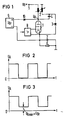
- FIG. 1 shows a circuit arrangement for preventing brake field vibrations of electron tubes using the example of a pulse duration modulation stage.
- the power supply 9 for generating the braking field voltage U Sr is connected in parallel with the switching tube 1 via a supply diode 10 connected between the anode of the switching tube 1, in this example a tetrode, and the positive pole of this voltage U Br .
- the supply voltage 5 (battery voltage U B ) is applied to the anode of the switching tube 1 via a pulse double choke 2, in one branch of which a coupling capacitor 4 is arranged.
- a freewheeling diode 3 is connected in parallel with the switching tube 1 between the cathode of the tube 1 and the pulse double choke 2.
- the control amplifier 8 is connected in parallel to the cathode and the control grid of the switching tube 1.
- the pulse duration modulated signal is supplied to the consumer 6 (transmitter output stage), to which a filter capacitor 7 is connected in parallel.
- Fig. 2 shows a diagram of the anode voltage profile U A of the switching tube 1 of the embodiment without power supply 9 and supply diode 10 for the braking field voltage Usr.
- FIG 3 shows a diagram of the anode voltage profile U A of the switching tube 1 of the exemplary embodiment according to the invention with a power supply unit 9 and a supply diode 10 for the braking field voltage U Br .
Landscapes
- Microwave Tubes (AREA)
- Emergency Protection Circuit Devices (AREA)
- Amplifiers (AREA)
- Dc-Dc Converters (AREA)
- Transmitters (AREA)
Claims (1)
Applications Claiming Priority (2)
| Application Number | Priority Date | Filing Date | Title |
|---|---|---|---|
| DE3331267 | 1983-08-30 | ||
| DE19833331267 DE3331267A1 (de) | 1983-08-30 | 1983-08-30 | Schaltungsanordnung zur verhinderung von bremsfeldschwingungen in elektronenroehren, insbesondere fuer eine pulsdauermodulationsstufe in sendeanlagen |
Publications (2)
| Publication Number | Publication Date |
|---|---|
| EP0141925A1 EP0141925A1 (fr) | 1985-05-22 |
| EP0141925B1 true EP0141925B1 (fr) | 1987-11-25 |
Family
ID=6207815
Family Applications (1)
| Application Number | Title | Priority Date | Filing Date |
|---|---|---|---|
| EP84109461A Expired EP0141925B1 (fr) | 1983-08-30 | 1984-08-08 | Montage pour supprimer les oscillations de champ retardateur dans des tubes électroniques, en particulier pour un étage de modulation de durée d'impulsion d'un arrangement émetteur |
Country Status (4)
| Country | Link |
|---|---|
| US (1) | US4720683A (fr) |
| EP (1) | EP0141925B1 (fr) |
| JP (1) | JPS6070818A (fr) |
| DE (2) | DE3331267A1 (fr) |
Family Cites Families (7)
| Publication number | Priority date | Publication date | Assignee | Title |
|---|---|---|---|---|
| DE568768C (de) * | 1933-01-23 | Ernst Gerhard Dr | Verfahren zur Frequenzvervielfachung elektrischer Wechselstroeme | |
| US2854574A (en) * | 1950-04-13 | 1958-09-30 | Sperry Rand Corp | Signal cycling device |
| DE949831C (de) * | 1954-12-31 | 1956-09-27 | Siemens Ag | Schaltung zur Amplitudenmodulation, bei der eine Hochfrequenz- Verstaerkerroehre als Belastung der Modulatorroehre geschaltet ist |
| DE966030C (de) * | 1954-12-31 | 1957-07-04 | Siemens Ag | Modulationsschaltung |
| US3179893A (en) * | 1961-11-08 | 1965-04-20 | Sylvania Electric Prod | Variable pulse width generator controlled by varying of d.c. screen grid potential |
| US3158815A (en) * | 1962-07-24 | 1964-11-24 | John P Hoice | Barkhausen oscillation elimination means |
| DE2715133C3 (de) * | 1977-04-05 | 1980-01-24 | Licentia Patent-Verwaltungs-Gmbh, 6000 Frankfurt | Modulationsverstärker |
-
1983
- 1983-08-30 DE DE19833331267 patent/DE3331267A1/de not_active Withdrawn
-
1984
- 1984-08-08 EP EP84109461A patent/EP0141925B1/fr not_active Expired
- 1984-08-08 DE DE8484109461T patent/DE3467841D1/de not_active Expired
- 1984-08-27 JP JP59178180A patent/JPS6070818A/ja active Pending
-
1986
- 1986-07-18 US US06/888,264 patent/US4720683A/en not_active Expired - Fee Related
Also Published As
| Publication number | Publication date |
|---|---|
| EP0141925A1 (fr) | 1985-05-22 |
| DE3331267A1 (de) | 1985-03-14 |
| JPS6070818A (ja) | 1985-04-22 |
| US4720683A (en) | 1988-01-19 |
| DE3467841D1 (en) | 1988-01-07 |
Similar Documents
| Publication | Publication Date | Title |
|---|---|---|
| DE3634979C2 (de) | Anordnung zur Erhöhung der Ausgangsleistung eines mit niedriger Spannung betriebenen Verstärkers, insbesondere für Autoradios | |
| EP0025234A1 (fr) | Amplificateur de puissance basse fréquence et application à un émetteur à modulation d'amplitude | |
| DE2542980A1 (de) | Modulator fuer einen rf-verstaerker | |
| EP0108194B1 (fr) | Circuit amplificateur sélectif du type push-pull | |
| EP0162374A1 (fr) | Disposition de circuit pour convertisseur | |
| EP0050753A1 (fr) | Disposition de circuit pour alimenter un utilisateur en courant alternatif avec une tension alternative et plus particulièrement avec une tension sinusoidale | |
| EP0141925B1 (fr) | Montage pour supprimer les oscillations de champ retardateur dans des tubes électroniques, en particulier pour un étage de modulation de durée d'impulsion d'un arrangement émetteur | |
| DE2715133A1 (de) | Modulationsverstaerker | |
| EP0271703B1 (fr) | Emetteur radio à modulation d'amplitude | |
| DE1514342A1 (de) | Elektromagnetische Strahlablenkschaltung | |
| DE2557512A1 (de) | Verstaerker | |
| EP0263936B1 (fr) | Alimentation de puissance à commutation sur le circuit secondaire | |
| EP0101853B1 (fr) | Dispositif de délivrance de signaux à isolement galvanique pour un système de commande | |
| DE943360C (de) | Schaltungsanordnung fuer elektronische Signaltongeneratoren | |
| DE1524716B2 (de) | Schaltungsanordnung zur Erregung eines Magnetwandlerkopfes zur Aufzeichnung von Informationssignalen auf einen magnetischen Aufzeichnungsträger | |
| DE2843733A1 (de) | Schaltung zur impulsversorgung einer elektronenstrahlroehre | |
| DE665633C (de) | Verfahren zur Modulation einer Gleich- oder Wechselspannung | |
| DE2831730C3 (de) | Modulations-Schaltung | |
| EP0582599B1 (fr) | Circuit pour la stabilisation de la haute tension dans un recepteur de television | |
| EP0215197B1 (fr) | Amplificateur vidéo de puissance et son circuit d'alimentation | |
| EP0038440B1 (fr) | Etage de commutation pour le controle d'une tetrode | |
| EP0382307A2 (fr) | Dispositif d'alimentation de puissance à commutation | |
| DE1090720B (de) | Gegentaktverstaerkeranordnung mit zwei gegenphasig ausgesteuerten, bezueglich des Anodenruhestromes in Serie geschalteten Roehren | |
| DE1120522B (de) | Antennenverstaerker | |
| DE2303988C3 (de) | Schaltungsanordnung zur Erzeugung einer hohen Gleichspannung aus einer niedrigen Gleichspannung |
Legal Events
| Date | Code | Title | Description |
|---|---|---|---|
| PUAI | Public reference made under article 153(3) epc to a published international application that has entered the european phase |
Free format text: ORIGINAL CODE: 0009012 |
|
| AK | Designated contracting states |
Designated state(s): CH DE FR GB LI NL |
|
| 17P | Request for examination filed |
Effective date: 19850807 |
|
| 17Q | First examination report despatched |
Effective date: 19861209 |
|
| GRAA | (expected) grant |
Free format text: ORIGINAL CODE: 0009210 |
|
| AK | Designated contracting states |
Kind code of ref document: B1 Designated state(s): CH DE FR GB LI NL |
|
| REF | Corresponds to: |
Ref document number: 3467841 Country of ref document: DE Date of ref document: 19880107 |
|
| ET | Fr: translation filed | ||
| GBT | Gb: translation of ep patent filed (gb section 77(6)(a)/1977) | ||
| PLBE | No opposition filed within time limit |
Free format text: ORIGINAL CODE: 0009261 |
|
| STAA | Information on the status of an ep patent application or granted ep patent |
Free format text: STATUS: NO OPPOSITION FILED WITHIN TIME LIMIT |
|
| 26N | No opposition filed | ||
| PG25 | Lapsed in a contracting state [announced via postgrant information from national office to epo] |
Ref country code: NL Effective date: 19900301 |
|
| NLV4 | Nl: lapsed or anulled due to non-payment of the annual fee | ||
| PGFP | Annual fee paid to national office [announced via postgrant information from national office to epo] |
Ref country code: GB Payment date: 19900719 Year of fee payment: 7 |
|
| PGFP | Annual fee paid to national office [announced via postgrant information from national office to epo] |
Ref country code: FR Payment date: 19900827 Year of fee payment: 7 |
|
| PGFP | Annual fee paid to national office [announced via postgrant information from national office to epo] |
Ref country code: DE Payment date: 19901025 Year of fee payment: 7 |
|
| PGFP | Annual fee paid to national office [announced via postgrant information from national office to epo] |
Ref country code: CH Payment date: 19901123 Year of fee payment: 7 |
|
| PG25 | Lapsed in a contracting state [announced via postgrant information from national office to epo] |
Ref country code: GB Effective date: 19910808 |
|
| PG25 | Lapsed in a contracting state [announced via postgrant information from national office to epo] |
Ref country code: LI Effective date: 19910831 Ref country code: CH Effective date: 19910831 |
|
| GBPC | Gb: european patent ceased through non-payment of renewal fee | ||
| PG25 | Lapsed in a contracting state [announced via postgrant information from national office to epo] |
Ref country code: FR Effective date: 19920430 |
|
| REG | Reference to a national code |
Ref country code: CH Ref legal event code: PL |
|
| PG25 | Lapsed in a contracting state [announced via postgrant information from national office to epo] |
Ref country code: DE Effective date: 19920501 |
|
| REG | Reference to a national code |
Ref country code: FR Ref legal event code: ST |