EP0141925B1 - Circuit for the suppression of retarding field oscillations in electronic tubes, especially for a pulse duration modulation stage of a transmitter system - Google Patents
Circuit for the suppression of retarding field oscillations in electronic tubes, especially for a pulse duration modulation stage of a transmitter system Download PDFInfo
- Publication number
- EP0141925B1 EP0141925B1 EP84109461A EP84109461A EP0141925B1 EP 0141925 B1 EP0141925 B1 EP 0141925B1 EP 84109461 A EP84109461 A EP 84109461A EP 84109461 A EP84109461 A EP 84109461A EP 0141925 B1 EP0141925 B1 EP 0141925B1
- Authority
- EP
- European Patent Office
- Prior art keywords
- voltage
- pulse duration
- modulation stage
- circuit
- retarding field
- Prior art date
- Legal status (The legal status is an assumption and is not a legal conclusion. Google has not performed a legal analysis and makes no representation as to the accuracy of the status listed.)
- Expired
Links
- 230000010355 oscillation Effects 0.000 title claims description 4
- 230000000979 retarding effect Effects 0.000 title claims 3
- 230000001629 suppression Effects 0.000 title 1
- 238000010586 diagram Methods 0.000 description 4
- 239000003990 capacitor Substances 0.000 description 2
- 230000008878 coupling Effects 0.000 description 1
- 238000010168 coupling process Methods 0.000 description 1
- 238000005859 coupling reaction Methods 0.000 description 1
- 238000013016 damping Methods 0.000 description 1
- 230000006866 deterioration Effects 0.000 description 1
- 230000000694 effects Effects 0.000 description 1
Images
Classifications
-
- H—ELECTRICITY
- H03—ELECTRONIC CIRCUITRY
- H03C—MODULATION
- H03C1/00—Amplitude modulation
- H03C1/16—Amplitude modulation by means of discharge device having at least three electrodes
-
- H—ELECTRICITY
- H03—ELECTRONIC CIRCUITRY
- H03K—PULSE TECHNIQUE
- H03K7/00—Modulating pulses with a continuously-variable modulating signal
- H03K7/08—Duration or width modulation ; Duty cycle modulation
Definitions
- the invention relates to a circuit arrangement for preventing brake field vibrations in electron tubes, in particular for a pulse duration modulation stage in transmitter systems.
- Brake field vibrations occur in both triodes and tetrodes.
- the present invention is therefore based on the object of providing a control circuit for avoiding the operating states which lead to the oscillation of the brake field vibrations.
- a power supply unit for generating a voltage for suppressing brake field vibrations is connected in parallel with the switching tube via a supply diode connected between the anode of the switching tube and the positive pole of this voltage.
- the circuit arrangement according to the invention ensures that the anode of the PDM switching tube does not fall below a predetermined voltage in any operating state, so that no braking field vibrations occur.
- the power to be applied by this power supply is low, so that the anode efficiency of the switching tube deteriorates only slightly.
- the effect of the circuit arrangement can be optimized by adapting the additional anode voltage source to the tube type.
- the size of the voltage U Sr (brake field voltage) is 50 to 300 V, depending on the tube type.
- the current depends on the power of the pulse duration modulation stage.
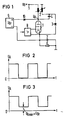
- FIG. 1 shows a circuit arrangement for preventing brake field vibrations of electron tubes using the example of a pulse duration modulation stage.
- the power supply 9 for generating the braking field voltage U Sr is connected in parallel with the switching tube 1 via a supply diode 10 connected between the anode of the switching tube 1, in this example a tetrode, and the positive pole of this voltage U Br .
- the supply voltage 5 (battery voltage U B ) is applied to the anode of the switching tube 1 via a pulse double choke 2, in one branch of which a coupling capacitor 4 is arranged.
- a freewheeling diode 3 is connected in parallel with the switching tube 1 between the cathode of the tube 1 and the pulse double choke 2.
- the control amplifier 8 is connected in parallel to the cathode and the control grid of the switching tube 1.
- the pulse duration modulated signal is supplied to the consumer 6 (transmitter output stage), to which a filter capacitor 7 is connected in parallel.
- Fig. 2 shows a diagram of the anode voltage profile U A of the switching tube 1 of the embodiment without power supply 9 and supply diode 10 for the braking field voltage Usr.
- FIG 3 shows a diagram of the anode voltage profile U A of the switching tube 1 of the exemplary embodiment according to the invention with a power supply unit 9 and a supply diode 10 for the braking field voltage U Br .
Landscapes
- Transmitters (AREA)
- Emergency Protection Circuit Devices (AREA)
- Amplifiers (AREA)
- Dc-Dc Converters (AREA)
- Microwave Tubes (AREA)
Description
Die Erfindung betrifft eine Schaltungsanordnung zur Verhinderung von Bremsfeldschwingungen in Elektronenröhren, insbesondere für eine Pulsdauermodulationsstufe in Sendeanlagen.The invention relates to a circuit arrangement for preventing brake field vibrations in electron tubes, in particular for a pulse duration modulation stage in transmitter systems.
Betreibt man Elektronenröhren im sogenannten überspannten Betrieb, d. h. die Anodenspannung liegt unter der Gitterspannung, dann treten bei entsprechenden Elektronendichten Bremsfeldschwingungen auf. Diese Schwingungen werden auch Barkhausen-Kurz-Schwingungen genannt (man vgl. Rint, Lexikon der Hochfrequenz-, Nachrichten- und Elektrotechnik, Bd. 1, 1957, Seiten 527 und 528). Die Frequenz dieser Schwingungen ist von den anliegenden Elektrodenspannungen abhängig.If one operates electron tubes in the so-called overvoltage mode, i. H. the anode voltage is below the grid voltage, then brake field vibrations occur with corresponding electron densities. These vibrations are also called Barkhausen short vibrations (cf. Rint, Lexikon der Hochfrequenz-, Nachrichten- und Elektrotechnik, vol. 1, 1957, pages 527 and 528). The frequency of these vibrations depends on the applied electrode voltages.
Bremsfeldschwingungen treten sowohl bei Trioden als auch bei Tetroden auf.Brake field vibrations occur in both triodes and tetrodes.
Durch äußere Dämpfung können diese Schwingungen nicht ververhindert werden. Man kann sie nur verhindern, indem man die Anodenspannung nicht so niedrig bzw. den Elektronenstrom nicht so hoch werden läßt, daß sich die Bremsfeldschwingungen ausbilden können.These vibrations cannot be prevented by external damping. It can only be prevented by not letting the anode voltage become so low or the electron current so high that the braking field vibrations can develop.
Das ist schaltungstechnisch in vielen Anwendungsfällen möglich. In sogenannten PDM- (Pulsdauermodulierten-) Sendern würden diese Maßnahmen zu einer Verschlechterung des Modulatorwirkungsgrades führen.In terms of circuitry, this is possible in many applications. In so-called PDM (pulse duration modulated) transmitters, these measures would lead to a deterioration in the modulator efficiency.
Der vorliegenden Erfindung liegt daher die Aufgabe zugrunde, eine Regelschaltung zum Vermeiden der Betriebszustände zu schaffen, die zum Anschwingen der Bremsfeldschwingungen führen.The present invention is therefore based on the object of providing a control circuit for avoiding the operating states which lead to the oscillation of the brake field vibrations.
Diese Aufgabe wird bei einer Schaltungsanordnung der eingangs genannten Art erfindungsgemäß dadurch gelöst, daß ein Netzteil zur Erzeugung einer Spannung zur Unterdrückung von Bremsfeldschwingungen über eine zwischen der Anode der Schaltröhre und dem positiven Pol dieser Spannung eingeschalteten Zuführungsdiode parallel zu der Schaltröhre geschaltet ist.This object is achieved according to the invention in a circuit arrangement of the type mentioned at the outset in that a power supply unit for generating a voltage for suppressing brake field vibrations is connected in parallel with the switching tube via a supply diode connected between the anode of the switching tube and the positive pole of this voltage.
Durch die erfindungsgemäße Schaltungsanordnung wird erreicht, daß die Anode der PDM-Schaltröhre in keinem Betriebszustand eine vorgegebene Spannung unterschreitet, so daß keine Bremsfeldschwingungen auftreten. Die durch diese Stromversorgung aufzubringende Leistung ist niedrig, so daß sich der Anodenwirkungsgrad der Schaltröhre nur wenig verschlechtert. Durch die Anpassung der zusätzlichen Anodenspannungsquelle an die Röhrentype kann die Wirkung der Schaltungsanordnung optimiert werden. Die Größe der Spannung USr (Bremsfeldspannung) liegt je nach Röhrentyp bei 50 bis 300 V. Der Strom ist von der Leistung der Pulsdauermodulationsstufe abhängig.The circuit arrangement according to the invention ensures that the anode of the PDM switching tube does not fall below a predetermined voltage in any operating state, so that no braking field vibrations occur. The power to be applied by this power supply is low, so that the anode efficiency of the switching tube deteriorates only slightly. The effect of the circuit arrangement can be optimized by adapting the additional anode voltage source to the tube type. The size of the voltage U Sr (brake field voltage) is 50 to 300 V, depending on the tube type. The current depends on the power of the pulse duration modulation stage.
Weitere Einzelheiten der Erfindung werden anhand eines in den Figuren der Zeichnung dargestellten Ausführungsbeispiels näher erläutert.Further details of the invention are explained in more detail with reference to an embodiment shown in the figures of the drawing.
Dabei zeigen:
- Fig. 1 Eine Schaltungsanordnung gemäß der Erfindung,
- Fig. 2 ein Diagramm des Anodenspannungsverlaufs ohne Netzteil und Zuführungsdiode für die Bremsfeldspannung gemäß der Schaltungsanordnung nach Fig. 1 und
- Fig. 3 ein Diagramm über den Anodenspannungsverlauf der erfindungsgemäßen Schaltungsanordnung.
- 1 shows a circuit arrangement according to the invention,
- Fig. 2 is a diagram of the anode voltage curve without power supply and feed diode for the brake field voltage according to the circuit arrangement of Fig. 1 and
- 3 shows a diagram of the anode voltage curve of the circuit arrangement according to the invention.
In Figur 1 ist eine Schaltungsanordnung zur Verhinderung von Bremsfeldschwingungen von Elektronenröhren am Beispiel einer Pulsdauermodulationsstufe dargestellt. Das Netzteil 9 zur Erzeugung der Bremsfeldspannung USr ist über eine zwischen der Anode der Schaltröhre 1, in diesem Beispiel einer Tetrode, und dem positiven Pol dieser Spannung UBr eingeschalteten zuführungsdiode 10 parallel zu der Schaltröhre 1 geschaltet. Die Versorgungsspannung 5 (Batteriespannung UB) ist an die Anode der Schaltröhre 1 über eine Impuls-Doppeldrossel 2 angelegt, in deren einem Zweig ein Koppelkondensator 4 angeordnet ist. Parallel zur Schaltröhre 1 ist zwischen der Kathode der Röhre 1 und der Impuls-Doppeldrossel 2 eine Freilaufdiode 3 geschaltet. Der Ansteuerverstärker 8 ist parallel zur Kathode und dem Steuergitter der Schaltröhre 1 geschaltet. Das pulsdauermodulierte Signal wird dem Verbraucher 6 (Senderendstufe), dem ein Siebkondensator 7 parallel geschaltet ist, zugeführt.FIG. 1 shows a circuit arrangement for preventing brake field vibrations of electron tubes using the example of a pulse duration modulation stage. The
Fig. 2 zeigt ein Diagramm über den Anodenspannungsverlauf UA der Schaltröhre 1 des Ausführungsbeispiels ohne Netzteil 9 und Zuführungsdiode 10 für die Bremsfeldspannung Usr.Fig. 2 shows a diagram of the anode voltage profile U A of the
Fig. 3 zeigt ein Diagramm über den Anodenspannungsverlauf UA der Schaltröhre 1 des erfindungsgemäßen Ausführungsbeispiels mit Netzteil 9 und Zuführungsdiode 10 für die Bremsfeldspannung UBr.3 shows a diagram of the anode voltage profile U A of the
Das Anodenspannungsminimum UA
Claims (1)
Applications Claiming Priority (2)
| Application Number | Priority Date | Filing Date | Title |
|---|---|---|---|
| DE19833331267 DE3331267A1 (en) | 1983-08-30 | 1983-08-30 | CIRCUIT ARRANGEMENT FOR PREVENTING BRAKE FIELD VIBRATIONS IN ELECTRON TUBES, ESPECIALLY FOR A PULSE DURATION MODULATION LEVEL IN TRANSMITTER SYSTEMS |
| DE3331267 | 1983-08-30 |
Publications (2)
| Publication Number | Publication Date |
|---|---|
| EP0141925A1 EP0141925A1 (en) | 1985-05-22 |
| EP0141925B1 true EP0141925B1 (en) | 1987-11-25 |
Family
ID=6207815
Family Applications (1)
| Application Number | Title | Priority Date | Filing Date |
|---|---|---|---|
| EP84109461A Expired EP0141925B1 (en) | 1983-08-30 | 1984-08-08 | Circuit for the suppression of retarding field oscillations in electronic tubes, especially for a pulse duration modulation stage of a transmitter system |
Country Status (4)
| Country | Link |
|---|---|
| US (1) | US4720683A (en) |
| EP (1) | EP0141925B1 (en) |
| JP (1) | JPS6070818A (en) |
| DE (2) | DE3331267A1 (en) |
Family Cites Families (7)
| Publication number | Priority date | Publication date | Assignee | Title |
|---|---|---|---|---|
| DE568768C (en) * | 1933-01-23 | Ernst Gerhard Dr | Method for frequency multiplication of electrical alternating currents | |
| US2854574A (en) * | 1950-04-13 | 1958-09-30 | Sperry Rand Corp | Signal cycling device |
| DE949831C (en) * | 1954-12-31 | 1956-09-27 | Siemens Ag | Circuit for amplitude modulation in which a high-frequency amplifier tube is connected to load the modulator tubes |
| DE966030C (en) * | 1954-12-31 | 1957-07-04 | Siemens Ag | Modulation circuit |
| US3179893A (en) * | 1961-11-08 | 1965-04-20 | Sylvania Electric Prod | Variable pulse width generator controlled by varying of d.c. screen grid potential |
| US3158815A (en) * | 1962-07-24 | 1964-11-24 | John P Hoice | Barkhausen oscillation elimination means |
| DE2715133C3 (en) * | 1977-04-05 | 1980-01-24 | Licentia Patent-Verwaltungs-Gmbh, 6000 Frankfurt | Modulation amplifier |
-
1983
- 1983-08-30 DE DE19833331267 patent/DE3331267A1/en not_active Withdrawn
-
1984
- 1984-08-08 EP EP84109461A patent/EP0141925B1/en not_active Expired
- 1984-08-08 DE DE8484109461T patent/DE3467841D1/en not_active Expired
- 1984-08-27 JP JP59178180A patent/JPS6070818A/en active Pending
-
1986
- 1986-07-18 US US06/888,264 patent/US4720683A/en not_active Expired - Fee Related
Also Published As
| Publication number | Publication date |
|---|---|
| DE3331267A1 (en) | 1985-03-14 |
| EP0141925A1 (en) | 1985-05-22 |
| JPS6070818A (en) | 1985-04-22 |
| DE3467841D1 (en) | 1988-01-07 |
| US4720683A (en) | 1988-01-19 |
Similar Documents
| Publication | Publication Date | Title |
|---|---|---|
| EP0025234A1 (en) | Low frequency power amplifier and its use in an amplitude modulated transmitter | |
| DE2542980A1 (en) | MODULATOR FOR AN RF AMPLIFIER | |
| EP0162374A1 (en) | Circuit arrangement for a converter | |
| EP0050753A1 (en) | Circuit arrangement to supply an alternative current user with an alternative voltage and more particularly with a sinous voltage | |
| EP0141925B1 (en) | Circuit for the suppression of retarding field oscillations in electronic tubes, especially for a pulse duration modulation stage of a transmitter system | |
| DE2715133A1 (en) | MODULATION AMPLIFIER | |
| DE102017213145A1 (en) | Method for operating a DC-DC converter | |
| EP0271703B1 (en) | Am radio transmitter | |
| DE1168951B (en) | Circuit with a transmitter for transmitting electrical pulses | |
| DE1514342A1 (en) | Electromagnetic beam deflection circuit | |
| DE2557512A1 (en) | AMPLIFIER | |
| EP0263936B1 (en) | Secondary side switchable power supply device | |
| EP0101853B1 (en) | Arrangement for delivering galvanically isolated signals for a control system | |
| DE943360C (en) | Circuit arrangement for electronic signal tone generators | |
| DE1524716B2 (en) | Circuit arrangement for exciting a magnetic transducer head for recording information signals on a magnetic recording medium | |
| DE2843733A1 (en) | CIRCUIT FOR THE PULSE SUPPLY OF AN ELECTRON BEAM TUBE | |
| DE665633C (en) | Method for modulating a direct or alternating voltage | |
| DE2831730C3 (en) | Modulation circuit | |
| EP0582599B1 (en) | Circuit for high voltage stabilization in a television receiver | |
| EP0215197B1 (en) | Video power amplifier and its supply | |
| EP0038440B1 (en) | Switching stage for controlling a tetrode | |
| EP0382307A2 (en) | Switching power supply device | |
| DE1090720B (en) | Push-pull amplifier arrangement with two tubes controlled in phase opposition and connected in series with regard to the anode quiescent current | |
| DE1120522B (en) | Antenna amplifier | |
| DE2303988C3 (en) | Circuit arrangement for generating a high DC voltage from a low DC voltage |
Legal Events
| Date | Code | Title | Description |
|---|---|---|---|
| PUAI | Public reference made under article 153(3) epc to a published international application that has entered the european phase |
Free format text: ORIGINAL CODE: 0009012 |
|
| AK | Designated contracting states |
Designated state(s): CH DE FR GB LI NL |
|
| 17P | Request for examination filed |
Effective date: 19850807 |
|
| 17Q | First examination report despatched |
Effective date: 19861209 |
|
| GRAA | (expected) grant |
Free format text: ORIGINAL CODE: 0009210 |
|
| AK | Designated contracting states |
Kind code of ref document: B1 Designated state(s): CH DE FR GB LI NL |
|
| REF | Corresponds to: |
Ref document number: 3467841 Country of ref document: DE Date of ref document: 19880107 |
|
| ET | Fr: translation filed | ||
| GBT | Gb: translation of ep patent filed (gb section 77(6)(a)/1977) | ||
| PLBE | No opposition filed within time limit |
Free format text: ORIGINAL CODE: 0009261 |
|
| STAA | Information on the status of an ep patent application or granted ep patent |
Free format text: STATUS: NO OPPOSITION FILED WITHIN TIME LIMIT |
|
| 26N | No opposition filed | ||
| PG25 | Lapsed in a contracting state [announced via postgrant information from national office to epo] |
Ref country code: NL Effective date: 19900301 |
|
| NLV4 | Nl: lapsed or anulled due to non-payment of the annual fee | ||
| PGFP | Annual fee paid to national office [announced via postgrant information from national office to epo] |
Ref country code: GB Payment date: 19900719 Year of fee payment: 7 |
|
| PGFP | Annual fee paid to national office [announced via postgrant information from national office to epo] |
Ref country code: FR Payment date: 19900827 Year of fee payment: 7 |
|
| PGFP | Annual fee paid to national office [announced via postgrant information from national office to epo] |
Ref country code: DE Payment date: 19901025 Year of fee payment: 7 |
|
| PGFP | Annual fee paid to national office [announced via postgrant information from national office to epo] |
Ref country code: CH Payment date: 19901123 Year of fee payment: 7 |
|
| PG25 | Lapsed in a contracting state [announced via postgrant information from national office to epo] |
Ref country code: GB Effective date: 19910808 |
|
| PG25 | Lapsed in a contracting state [announced via postgrant information from national office to epo] |
Ref country code: LI Effective date: 19910831 Ref country code: CH Effective date: 19910831 |
|
| GBPC | Gb: european patent ceased through non-payment of renewal fee | ||
| PG25 | Lapsed in a contracting state [announced via postgrant information from national office to epo] |
Ref country code: FR Effective date: 19920430 |
|
| REG | Reference to a national code |
Ref country code: CH Ref legal event code: PL |
|
| PG25 | Lapsed in a contracting state [announced via postgrant information from national office to epo] |
Ref country code: DE Effective date: 19920501 |
|
| REG | Reference to a national code |
Ref country code: FR Ref legal event code: ST |