EP0138563A2 - Lateraler Transistor - Google Patents
Lateraler Transistor Download PDFInfo
- Publication number
- EP0138563A2 EP0138563A2 EP84306893A EP84306893A EP0138563A2 EP 0138563 A2 EP0138563 A2 EP 0138563A2 EP 84306893 A EP84306893 A EP 84306893A EP 84306893 A EP84306893 A EP 84306893A EP 0138563 A2 EP0138563 A2 EP 0138563A2
- Authority
- EP
- European Patent Office
- Prior art keywords
- region
- base
- transistor
- collector
- base region
- Prior art date
- Legal status (The legal status is an assumption and is not a legal conclusion. Google has not performed a legal analysis and makes no representation as to the accuracy of the status listed.)
- Withdrawn
Links
- 239000000758 substrate Substances 0.000 claims abstract description 30
- 239000012212 insulator Substances 0.000 claims abstract description 15
- 229910052710 silicon Inorganic materials 0.000 claims abstract description 10
- 239000010703 silicon Substances 0.000 claims abstract description 10
- 239000000969 carrier Substances 0.000 description 22
- VYPSYNLAJGMNEJ-UHFFFAOYSA-N Silicium dioxide Chemical compound O=[Si]=O VYPSYNLAJGMNEJ-UHFFFAOYSA-N 0.000 description 9
- XUIMIQQOPSSXEZ-UHFFFAOYSA-N Silicon Chemical compound [Si] XUIMIQQOPSSXEZ-UHFFFAOYSA-N 0.000 description 8
- 238000000034 method Methods 0.000 description 8
- 239000004065 semiconductor Substances 0.000 description 8
- 238000009826 distribution Methods 0.000 description 7
- 238000004519 manufacturing process Methods 0.000 description 6
- 230000003071 parasitic effect Effects 0.000 description 5
- 230000003321 amplification Effects 0.000 description 4
- 230000007423 decrease Effects 0.000 description 4
- 239000002019 doping agent Substances 0.000 description 4
- 238000003199 nucleic acid amplification method Methods 0.000 description 4
- 239000000377 silicon dioxide Substances 0.000 description 4
- ZOXJGFHDIHLPTG-UHFFFAOYSA-N Boron Chemical compound [B] ZOXJGFHDIHLPTG-UHFFFAOYSA-N 0.000 description 3
- 229910052796 boron Inorganic materials 0.000 description 3
- 238000010438 heat treatment Methods 0.000 description 3
- 235000012239 silicon dioxide Nutrition 0.000 description 3
- OAICVXFJPJFONN-UHFFFAOYSA-N Phosphorus Chemical compound [P] OAICVXFJPJFONN-UHFFFAOYSA-N 0.000 description 2
- 238000005229 chemical vapour deposition Methods 0.000 description 2
- 229910052681 coesite Inorganic materials 0.000 description 2
- 229910052906 cristobalite Inorganic materials 0.000 description 2
- 238000010586 diagram Methods 0.000 description 2
- 238000009792 diffusion process Methods 0.000 description 2
- 238000002513 implantation Methods 0.000 description 2
- 238000012856 packing Methods 0.000 description 2
- 230000002093 peripheral effect Effects 0.000 description 2
- 229910052698 phosphorus Inorganic materials 0.000 description 2
- 239000011574 phosphorus Substances 0.000 description 2
- 229910021420 polycrystalline silicon Inorganic materials 0.000 description 2
- 229910052682 stishovite Inorganic materials 0.000 description 2
- 229910052905 tridymite Inorganic materials 0.000 description 2
- 230000002411 adverse Effects 0.000 description 1
- 230000015572 biosynthetic process Effects 0.000 description 1
- 230000000295 complement effect Effects 0.000 description 1
- 239000012141 concentrate Substances 0.000 description 1
- 238000007796 conventional method Methods 0.000 description 1
- 230000000694 effects Effects 0.000 description 1
- 238000010894 electron beam technology Methods 0.000 description 1
- 238000005530 etching Methods 0.000 description 1
- 230000005669 field effect Effects 0.000 description 1
- 239000007943 implant Substances 0.000 description 1
- 238000002347 injection Methods 0.000 description 1
- 239000007924 injection Substances 0.000 description 1
- 239000002184 metal Substances 0.000 description 1
- 229910044991 metal oxide Inorganic materials 0.000 description 1
- 150000004706 metal oxides Chemical class 0.000 description 1
- 229910052760 oxygen Inorganic materials 0.000 description 1
- 239000001301 oxygen Substances 0.000 description 1
- -1 oxygen ions Chemical class 0.000 description 1
- 229920002120 photoresistant polymer Polymers 0.000 description 1
- 238000005215 recombination Methods 0.000 description 1
- 230000006798 recombination Effects 0.000 description 1
- 230000004083 survival effect Effects 0.000 description 1
Images


Classifications
-
- H—ELECTRICITY
- H01—ELECTRIC ELEMENTS
- H01L—SEMICONDUCTOR DEVICES NOT COVERED BY CLASS H10
- H01L29/00—Semiconductor devices adapted for rectifying, amplifying, oscillating or switching, or capacitors or resistors with at least one potential-jump barrier or surface barrier, e.g. PN junction depletion layer or carrier concentration layer; Details of semiconductor bodies or of electrodes thereof ; Multistep manufacturing processes therefor
- H01L29/66—Types of semiconductor device ; Multistep manufacturing processes therefor
- H01L29/66007—Multistep manufacturing processes
- H01L29/66075—Multistep manufacturing processes of devices having semiconductor bodies comprising group 14 or group 13/15 materials
- H01L29/66227—Multistep manufacturing processes of devices having semiconductor bodies comprising group 14 or group 13/15 materials the devices being controllable only by the electric current supplied or the electric potential applied, to an electrode which does not carry the current to be rectified, amplified or switched, e.g. three-terminal devices
- H01L29/66234—Bipolar junction transistors [BJT]
- H01L29/66265—Thin film bipolar transistors
-
- H—ELECTRICITY
- H01—ELECTRIC ELEMENTS
- H01L—SEMICONDUCTOR DEVICES NOT COVERED BY CLASS H10
- H01L25/00—Assemblies consisting of a plurality of individual semiconductor or other solid state devices ; Multistep manufacturing processes thereof
-
- H—ELECTRICITY
- H01—ELECTRIC ELEMENTS
- H01L—SEMICONDUCTOR DEVICES NOT COVERED BY CLASS H10
- H01L29/00—Semiconductor devices adapted for rectifying, amplifying, oscillating or switching, or capacitors or resistors with at least one potential-jump barrier or surface barrier, e.g. PN junction depletion layer or carrier concentration layer; Details of semiconductor bodies or of electrodes thereof ; Multistep manufacturing processes therefor
- H01L29/02—Semiconductor bodies ; Multistep manufacturing processes therefor
- H01L29/06—Semiconductor bodies ; Multistep manufacturing processes therefor characterised by their shape; characterised by the shapes, relative sizes, or dispositions of the semiconductor regions ; characterised by the concentration or distribution of impurities within semiconductor regions
- H01L29/10—Semiconductor bodies ; Multistep manufacturing processes therefor characterised by their shape; characterised by the shapes, relative sizes, or dispositions of the semiconductor regions ; characterised by the concentration or distribution of impurities within semiconductor regions with semiconductor regions connected to an electrode not carrying current to be rectified, amplified or switched and such electrode being part of a semiconductor device which comprises three or more electrodes
- H01L29/1004—Base region of bipolar transistors
- H01L29/1008—Base region of bipolar transistors of lateral transistors
-
- H—ELECTRICITY
- H01—ELECTRIC ELEMENTS
- H01L—SEMICONDUCTOR DEVICES NOT COVERED BY CLASS H10
- H01L29/00—Semiconductor devices adapted for rectifying, amplifying, oscillating or switching, or capacitors or resistors with at least one potential-jump barrier or surface barrier, e.g. PN junction depletion layer or carrier concentration layer; Details of semiconductor bodies or of electrodes thereof ; Multistep manufacturing processes therefor
- H01L29/66—Types of semiconductor device ; Multistep manufacturing processes therefor
- H01L29/68—Types of semiconductor device ; Multistep manufacturing processes therefor controllable by only the electric current supplied, or only the electric potential applied, to an electrode which does not carry the current to be rectified, amplified or switched
- H01L29/70—Bipolar devices
- H01L29/72—Transistor-type devices, i.e. able to continuously respond to applied control signals
- H01L29/73—Bipolar junction transistors
- H01L29/7317—Bipolar thin film transistors
-
- H—ELECTRICITY
- H01—ELECTRIC ELEMENTS
- H01L—SEMICONDUCTOR DEVICES NOT COVERED BY CLASS H10
- H01L29/00—Semiconductor devices adapted for rectifying, amplifying, oscillating or switching, or capacitors or resistors with at least one potential-jump barrier or surface barrier, e.g. PN junction depletion layer or carrier concentration layer; Details of semiconductor bodies or of electrodes thereof ; Multistep manufacturing processes therefor
- H01L29/66—Types of semiconductor device ; Multistep manufacturing processes therefor
- H01L29/68—Types of semiconductor device ; Multistep manufacturing processes therefor controllable by only the electric current supplied, or only the electric potential applied, to an electrode which does not carry the current to be rectified, amplified or switched
- H01L29/70—Bipolar devices
- H01L29/72—Transistor-type devices, i.e. able to continuously respond to applied control signals
- H01L29/73—Bipolar junction transistors
- H01L29/735—Lateral transistors
Definitions
- the present invention relates to lateral transistors.
- lateral refers to a direction parallel to a surface of a (semiconductor) substrate (in which a “lateral” transistor is formed) and “vertical” refers to a direction perpendicular to the surface of the substrate.
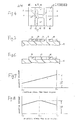
- FIG. 1 A schematic cross-sectional view of a basic structure of a previously proposed lateral transistor, formed in a semiconductor substrate of an integrated circuit (IC) semiconductor device, is illustrated in Fig. 1.
- the structure differs most radically from other (vertical) transistor structures in that transistor action is performed in a lateral direction rather than in a vertical direction.
- a lateral transistor is used advantageously, because of its simple structure, for example in building a pnp transistor in the course of processes for fabricating an npn structure, or vice versa, without requiring an additional process.
- MIS metal insulator silicon
- FET field effect transistors
- a bipolar transistor is suitable for driving elements for peripheral circuits to such an IC.
- Such driving elements are required to provide high current outputs because of parasitic capacitances associated with wiring interconnections to peripheral circuits.
- MIS transistors are used for such driving elements, they occupy areas of significant size as MIS transistors have low transconductance. This has an adverse effect on the level of packing density which can be achieved. Accordingly, a combination of MIS transistors and lateral (bipolar) transistors may be expected to be effective when employed in such a semiconductor device (IC).
- a previously proposed lateral transistor has a structure as shown in Fig. 1, in which an emitter region E and a collector region C, formed with n type doping for example, are formed separately in a p-type doped base region B formed in a substrate S. Carriers from the emitter region E are transported in all directions in the base region B (as indicated by arrows in Fig. 1) and most of the carriers fail to reach the collector region. This means that the transportation efficiency of carriers in the base region is low, resulting in a low current amplification factor for the lateral transistor structure. In addition, parasitic capacitances are so high as to result in a low switching speed for the lateral transistor.
- lateral transistor structures have been proposed in which the base region, except for a portion thereof positioned between emitter and collector regions, is removed by etching, or in which all regions are formed on an insulator I or an SOI substrate for example as shown in the schematic cross-sectional view of Fig. 2 and the corresponding plan view of Fig. 3.
- base width As shown in Fig. 3, for the emitter region E and the collector region C, electrode structures having a contact hole, He or Hc, opened in an insulator layer covering the relevant region, are used. However such a structure as employed for emitter and collector regions is not applicable to the base region B because of its narrow base width.
- the base region accordingly, is extended in a longitudinal direction to an outside area (beyond the emitter and collector regions), where a contact hole Hb is formed for a base electrode.
- the longitudinal resistance of the base region B as seen from the base contact becomes high, causing the actual base-emitter junction voltage along the junction to drop below the value expected from the externally applied voltages. This results in decrease in efficiency of injection of carriers from the emitter region E to the base region B. Hence, the characteristics of the transistor are seriously degraded.
- a lateral bipolar transistor having a structure with a base region, a base contact region, an emitter region and a collector region, the base region comprising:
- An embodiment of the present invention can provide a lateral transistor formed on a silicon on insulator (SOI) substrate with an enhanced current amplification factor.
- SOI silicon on insulator
- An'embodiment of the present invention can provide a lateral transistor with a high current transconductance.
- An embodiment of the present invention can provide a bipolar lateral transistor having a base region structure such as to reduce the voltage drop along the emitter-base junction.
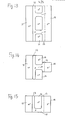
- a base region is comprised of two parts called here a first base region 13 and a second base region 15, 17.
- the second base region is considered as divided roughly into two portions 15 and 17 as shown in Fig. 4.
- 17 denotes a "connecting" portion of the second base region which serves to connect the first base region 13 to base contact 16 of the transistor.
- the first base region 13 generally corresponds to the base region of a previously proposed lateral transistor.
- the first base region has a narrow base width such as one pm.
- the second base region 15(17) plays the role of a connecting portion for the first region 13 and extends from the first base region in a lateral direction.
- the second base region 15(17) will, usually, be of the same dopant density as that of the first base region 13 and (the connecting portion 17) of greater width, for example three to four ⁇ m.
- the second base region is in this way, for example, provided with a significantly lower longitudinal resistance than that of the first base region 13.
- the first base region 13 forms the base-emitter junction with an emitter region 12 and a base-collector junction with a collector region 14.
- the second base region (connecting portion 17) runs across the collector region 14 of the transistor dividing it into two or more portions (sub-collector regions).
- the second base region shares a part of the collector-base junction with the collector region 14.
- the second base region 15 joins base contact region 16 which is highly dosed and plate the role of a contact area for the whole base region. This is effective to enhance the current amplification factor of the lateral transistor in comparison with the previously proposed lateral transistor. The reason is as follows.
- the graphs of Fig. 7 and Fig. 8 illustrate respectively base-emitter junction voltage distribution along the line X-X of the base region B shown in Fig. 3 and voltage distribution along the line Y-Y of the first base region 13 shown in Fig. 4, when an external voltage Vb is applied to the base contacts of those regions.
- the base width (of region B and of first base region 13) is very narrow, providing a high longitudinal resistance.
- the voltage distribution shows a considerable sharp drop along the base region. Therefore, the voltage applied to the base-emitter junction decreases from the point Bc, where the base contact is connected, toward the end of the junction Be.
- Fig. 13 illustrates an embodiment having two second base regions. With such a structure, the total drop of the base-emitter voltage can be reduced further.
- emitter-base and collector-base parasitic capacities become small, providing a transistor with a higher switching speed.
- a bipolar lateral transistor in accordance with an embodiment of the present invention having a high current amplification factor is useful to save the space on a substrate by replacing MOS-type elements.
- the ease of fabrication of a lateral transistor into IC devices is also a substantial advantage.
- a twinned lateral bipolar transistor can be obtained in accordance with an embodiment of the present invention, for example having providing two lateral bipolar transistors with a common emitter electrode or common collector electrode.
- Such a twinned lateral transistor is particularly suitable for a driving element of an IC device for circuits to drive associated circuits.
- a SOI (silicon on insulator) substrate comprises an insulator layer 10 and a monocrystal silicon layer (not shown).
- a silicon dioxide (SiO 2 > layer On the insulator layer 10, for example a silicon dioxide (SiO 2 > layer, a transistor region 11 of monocrystal silicon is formed.
- an n +- type doped emitter region 12 As shown in Fig. 4, an n +- type doped emitter region 12, a p-type doped first base region 13, an n +- type doped collector region 14, divided into two portions (sub-collector regions), a p-type doped second base region 15(17) and a p + - type-doped base contact region 16 are formed in the transistor region 11 using conventional semiconductor fabrication methods.
- the base region of the lateral transistor comprises the first base region 13 and the second base region 15 and has a base contact region 16.
- the first base region 13 plays substantially the same part as the base region B of the previously proposed lateral transistor.
- the first base region 13 forms the base-emitter junction of the transistor. (The first base region 13 forms only part of the base-collector junction).
- the first base region l3. has an extremely small base width, for example in the order of 1 to 2 um, to reduce loss of carriers injected through the emitter-base junction during their travel through the first base region 13.
- the second base region 15 includes connecting portion 17, which serves for connecting the first base region 13 and the base contact region 16.
- the width of the connecting portion 17 is greater than that of the first base region 13, for example in the order of 3 to 4 um, to reduce resistance in its longitudinal direction to reduce voltage drop, due to base current, between the first base region 13 and the base contact region 16.
- Base-collector junctions are formed along the boundary between the collector region 14 (sub-collector regions) and the base region 13, 17, and 15 as shown in Fig. 4. Most carriers injected into the first base region 13 (from the emitter region 12) travel through the first base region 13 to reach the collector region 14. However, carriers injected through the emitter-base junction where it encounters (faces) the connecting portion 17 of the second base region 15 (see the hatched portion of the junction labelled M in Fig. 4) become stray carriers which fail to reach the collector region 14 (across the base region 13). Nevertheless, as stated above junctions formed along the boundary between the collector region 14 and the connecting portion 17 can absorb the stray carriers at corners of the collector region 14, labelled N in Fig. 4. Considering that the emitter-base junction voltage is highest at the hatched portion M (see Fig. 8) the survival (absorbtion) of such stray carriers is effective to enhance the number of carriers reaching the collector 14.
- the connecting portion 17 of the second base region divides the collector region 14 into two portions (sub-collector regions) each of geneally rectangular shape.
- each region contacts the insulator layer 10 preventing the loss of the carriers in the vertical direction, and also the parasitic capacities associated with each region or the substrate is significantly small providing the lateral transistor with high speed switching ability.
- the voltage actually applied to the emitter-base junction will be discussed now. As described above, there is a significant voltage drop along the junction (moving away from the base contact region) due to the base current because of the high resistance of the first-base region 13 in its longitudinal direction.
- the graph of Fig. 7 schematically illustrates junction voltage distribution along the base-emitter junction for the lateral transistor of Fig. 3 and the graph of Fig. 8 schematically illustrates junction voltage distribution along the base-emitter junction of the lateral transistor of Fig. 4.
- reference Bc denotes the position along the base-emitter junction nearest to the base contact, to which an external base voltage V b is applied
- reference Be denotes the position of an end of the junction (away from the base contact).
- base current Ib and applied base voltage V b are the same in relation to both Figures and it is assumed that longitudinal base resistivity (i.e. resistivity of the base region B in Fig. 3 and resistivity of first base region 13 in Fig. 4) is uniformly distributed and the same in relation to both Figures. From these curves, in the graphs of Figs. 7 and 8, it is clear that the lateral transistor of Fig. 4, an embodiment of the present invention, has a higher effective emitter-base junction voltage in total (overall). Accordingly, the carrier emitter efficiency is significantly improved as the number of carriers increases exponentially in proportion to the voltage applied to the junction.
- a SOI substrate is prepared.
- a transistor region formed of a silicon monocrystal layer 11 of 0.5 to 1.0 pm thick is provided on an insulating layer 10 as shown in Fig. 9.
- One method is to form a polycrystalline silicon layer (on an insulating layer) by a conventional chemical vapour deposition (CVD) method and then to recrystallize the polycrystalline silicon layer by heating with a laser beam, an electron beam, an infrared beam, etc. to convert its structure to a monocrystal structure.
- CVD chemical vapour deposition
- Another method is to implant oxygen ions into a monocrystal substrate so that they concentrate at a specified depth below the surface of the substrate and to heat the substrate to form a silicon dioxide layer inside the substrate whilst retaining a monocrystal layer at the surface of the substrate.
- field oxide regions (not shown) of silicon dioxide (Si0 2 ) can be formed in the silicon monocrystal layer to define (laterally) the transistor region.
- the (whole) transistor region 11 is doped by implanting boron (B), for example, with a dose of 5 X 10 12 ⁇ 14 atm/cm 2 at 40 to 60 Kev and heating the substrate at approximately 1050°C to diffuse the implanted dopant to form a diffusion region of around 10 16 ⁇ 18 atm/cm 3 concentration (p-type doped region). Then, as shown in Fig.
- boron (B) dopants are again implanted again with a dose of around 10 15 atm/cm 2 at 40 to 60 Kev, and the dopants are diffused to form the base contact region of 10 19 ⁇ 20 atm/cm concentration.
- the substrate is covered again by a photoresist layer 19 as shown in Fig. 11, and a phosphorus implantation is effected with a dose of 5 X 10 15 a t m/cm 2 and then heating is effected to form n-type diffusion regions of almost 10 20 atm/cm 3 concentration which provide emitter region 12 and divided collector region portions (sub-collector regions) 14.
- an insulator layer 21, and conductive paths 20 for the emitter region 12, the collector region 14 and the base contact region 16 are formed to finish a lateral bipolar transistor as shown in Fig. 12.
- FIG. 13 A plan view of the resulting lateral bipolar transistor having a base region structure in accordance with an embodiment of the prensent invention is illustrated in Fig. 13. It will be noted that this structure has two connecting portions 17 (as compared with only a single such portion in Fig. 4) for the base region, providing the emitter-base junction with further enhanced voltage to increase the emitter efficiency of the carriers in the first base region.
- This type of transistor structure is suitable for use in a relatively large type lateral transistor for handling high current.
- FIG. 14 Another lateral transistor embodying the present invention is illustrated in Fig. 14 which has a reduced base contact region 16 (as compared with the transistor of Fig. 4) sufficient only to form a base contact, with the aim of saving space on the substrate.
- FIG. 15 shows a different, simple lateral transistor structure which is suitable for forming a small type transistor embodying the present invention.
- the second base region differs from that seen in Fig. 4.
- Fig. 16 and Fig. 17 illustrate further embodiments of the present in each of which two lateral transistor structures as shown in Fig. 15 are joined to form twinned lateral transistors.
- the twinned transistors have a common emitter region 12.
- the twinned transistors have common base contact region 16, namely, a common base contact.
- Such twinned lateral transistors are particularly suitable for saving space on the surface of an IC substrate to provide higher packing density and also saving IC fabrication costs.
- Fig. 18 is a schematic circuit diagram of a circuit utilizing a npn lateral transistor 23 and a pnp lateral transistor 24 together with C MOS transistors 25.
- the lateral transistors 23 and 24 can be fabricated using the same fabricating process as is used for the C MOS transistors 25 without the need for additional fabrication steps.
- the lateral transistors according to the present invention are most suitable for an output circuit of a C MOS (complementary metal oxide semiconductor) IC.
- C MOS complementary metal oxide semiconductor
- the base region and base contact region can be of a first conductivity type (either n or p) and the collector and emitter regions of a second (opposite) conductivity type (p or n).
- the second base region connects the first base region to the base contact region and extends along the collector region.
- the base, emitter and collector region are in surface - to surface contact with an underlying insulator of an SOI substrate.
- lateral transistors 23 and 24 in Fig. 18 can be provided by twinned lateral transistors as illustrated in Figs. 16 and 17.
- An embodiment of the present invention provides a lateral bipolar transistor formed on a silicon on insulator (SOI) substrate, having a base region, a base contact region, an emitter region and a collector region.
- the base region comprises a first base region having a narrow base width and sharing an emitter-base junction with the emitter region.
- the base region also comprises a second base region extending laterally and partially surrounding the collector region and sharing a base-collector junction with the collector region.
- the base contact region is connected to the first base region (via the second base region).
- the connecting portion (17) of the second base region extends transversely (e.g. perpendicularly) of the longitudinal extent of the first base region.
Applications Claiming Priority (2)
| Application Number | Priority Date | Filing Date | Title |
|---|---|---|---|
| JP58191188A JPS6081864A (ja) | 1983-10-12 | 1983-10-12 | ラテラル型トランジスタ |
| JP191188/83 | 1983-10-12 |
Publications (2)
| Publication Number | Publication Date |
|---|---|
| EP0138563A2 true EP0138563A2 (de) | 1985-04-24 |
| EP0138563A3 EP0138563A3 (de) | 1987-01-28 |
Family
ID=16270360
Family Applications (1)
| Application Number | Title | Priority Date | Filing Date |
|---|---|---|---|
| EP84306893A Withdrawn EP0138563A3 (de) | 1983-10-12 | 1984-10-10 | Lateraler Transistor |
Country Status (3)
| Country | Link |
|---|---|
| EP (1) | EP0138563A3 (de) |
| JP (1) | JPS6081864A (de) |
| KR (1) | KR850003478A (de) |
Cited By (7)
| Publication number | Priority date | Publication date | Assignee | Title |
|---|---|---|---|---|
| EP0396802A1 (de) * | 1989-05-11 | 1990-11-14 | Siemens Aktiengesellschaft | Verfahren zur Herstellung einer integrierten Schaltungsstruktur mit einem lateralen Bipolartransistor |
| US5075737A (en) * | 1987-06-16 | 1991-12-24 | Nissan Motor Co., Ltd. | Thin film semiconductor device |
| EP0465227A2 (de) * | 1990-07-02 | 1992-01-08 | Kabushiki Kaisha Toshiba | Zusammengesetzte integrierte Schaltungsanordnung |
| EP0632490A2 (de) * | 1993-07-02 | 1995-01-04 | Siemens Aktiengesellschaft | Herstellungsverfahren für lateralen Bipolartransistor |
| EP0632491A2 (de) * | 1993-07-02 | 1995-01-04 | Siemens Aktiengesellschaft | Herstellungsverfahren für lateralen Bipolartransistor |
| EP0632489A2 (de) * | 1993-07-02 | 1995-01-04 | Siemens Aktiengesellschaft | Herstellungsverfahren für lateralen Bipolartransistor |
| US5994739A (en) * | 1990-07-02 | 1999-11-30 | Kabushiki Kaisha Toshiba | Integrated circuit device |
Citations (4)
| Publication number | Priority date | Publication date | Assignee | Title |
|---|---|---|---|---|
| US3513042A (en) * | 1965-01-15 | 1970-05-19 | North American Rockwell | Method of making a semiconductor device by diffusion |
| EP0052038A2 (de) * | 1980-10-23 | 1982-05-19 | FAIRCHILD CAMERA & INSTRUMENT CORPORATION | Herstellungsverfahreneiner integrierten Schaltkreisstruktur |
| EP0060761A1 (de) * | 1981-03-13 | 1982-09-22 | Societe Pour L'etude Et La Fabrication De Circuits Integres Speciaux - E.F.C.I.S. | Lateraler bipolarer Transistor auf Isolator und Verfahren zu seiner Herstellung |
| EP0068072A2 (de) * | 1981-07-01 | 1983-01-05 | Rockwell International Corporation | Lateraler PNP Transistor und Herstellungsverfahren |
-
1983
- 1983-10-12 JP JP58191188A patent/JPS6081864A/ja active Pending
-
1984
- 1984-10-10 KR KR1019840006240A patent/KR850003478A/ko not_active IP Right Cessation
- 1984-10-10 EP EP84306893A patent/EP0138563A3/de not_active Withdrawn
Patent Citations (4)
| Publication number | Priority date | Publication date | Assignee | Title |
|---|---|---|---|---|
| US3513042A (en) * | 1965-01-15 | 1970-05-19 | North American Rockwell | Method of making a semiconductor device by diffusion |
| EP0052038A2 (de) * | 1980-10-23 | 1982-05-19 | FAIRCHILD CAMERA & INSTRUMENT CORPORATION | Herstellungsverfahreneiner integrierten Schaltkreisstruktur |
| EP0060761A1 (de) * | 1981-03-13 | 1982-09-22 | Societe Pour L'etude Et La Fabrication De Circuits Integres Speciaux - E.F.C.I.S. | Lateraler bipolarer Transistor auf Isolator und Verfahren zu seiner Herstellung |
| EP0068072A2 (de) * | 1981-07-01 | 1983-01-05 | Rockwell International Corporation | Lateraler PNP Transistor und Herstellungsverfahren |
Cited By (15)
| Publication number | Priority date | Publication date | Assignee | Title |
|---|---|---|---|---|
| US5075737A (en) * | 1987-06-16 | 1991-12-24 | Nissan Motor Co., Ltd. | Thin film semiconductor device |
| US5047823A (en) * | 1989-05-11 | 1991-09-10 | Siemens Aktiengesellschaft | Circuit structure having a lateral bipolar transistor and its method of manufacture |
| EP0396802A1 (de) * | 1989-05-11 | 1990-11-14 | Siemens Aktiengesellschaft | Verfahren zur Herstellung einer integrierten Schaltungsstruktur mit einem lateralen Bipolartransistor |
| EP0740338A2 (de) * | 1990-07-02 | 1996-10-30 | Kabushiki Kaisha Toshiba | Zusammengesetzte integrierte Schaltungsanordnung |
| EP0465227A2 (de) * | 1990-07-02 | 1992-01-08 | Kabushiki Kaisha Toshiba | Zusammengesetzte integrierte Schaltungsanordnung |
| EP0465227A3 (en) * | 1990-07-02 | 1992-10-07 | Kabushiki Kaisha Toshiba | Composite integrated circuit device |
| US5994739A (en) * | 1990-07-02 | 1999-11-30 | Kabushiki Kaisha Toshiba | Integrated circuit device |
| EP0740338A3 (de) * | 1990-07-02 | 1998-01-07 | Kabushiki Kaisha Toshiba | Zusammengesetzte integrierte Schaltungsanordnung |
| US5477065A (en) * | 1990-07-02 | 1995-12-19 | Kabushiki Kaisha Toshiba | Lateral thin film thyristor with bevel |
| EP0632491A2 (de) * | 1993-07-02 | 1995-01-04 | Siemens Aktiengesellschaft | Herstellungsverfahren für lateralen Bipolartransistor |
| EP0632491A3 (de) * | 1993-07-02 | 1996-09-11 | Siemens Ag | Herstellungsverfahren für lateralen Bipolartransistor. |
| EP0632489A3 (de) * | 1993-07-02 | 1996-09-11 | Siemens Ag | Herstellungsverfahren für lateralen Bipolartransistor. |
| EP0632490A3 (de) * | 1993-07-02 | 1996-09-11 | Siemens Ag | Herstellungsverfahren für lateralen Bipolartransistor. |
| EP0632489A2 (de) * | 1993-07-02 | 1995-01-04 | Siemens Aktiengesellschaft | Herstellungsverfahren für lateralen Bipolartransistor |
| EP0632490A2 (de) * | 1993-07-02 | 1995-01-04 | Siemens Aktiengesellschaft | Herstellungsverfahren für lateralen Bipolartransistor |
Also Published As
| Publication number | Publication date |
|---|---|
| KR850003478A (ko) | 1985-06-17 |
| JPS6081864A (ja) | 1985-05-09 |
| EP0138563A3 (de) | 1987-01-28 |
Similar Documents
| Publication | Publication Date | Title |
|---|---|---|
| US3962717A (en) | Oxide isolated integrated injection logic with selective guard ring | |
| US4038680A (en) | Semiconductor integrated circuit device | |
| US5416354A (en) | Inverted epitaxial process semiconductor devices | |
| JPH06151723A (ja) | モノリシック半導体素子のバイポーラトランジスタ構造、及び前記モノリシック半導体素子の製造方法 | |
| US3993513A (en) | Combined method for fabricating oxide-isolated vertical bipolar transistors and complementary oxide-isolated lateral bipolar transistors and the resulting structures | |
| US5714793A (en) | Complementary vertical bipolar junction transistors formed in silicon-on-saphire | |
| US3766449A (en) | Transistors | |
| US4390890A (en) | Saturation-limited bipolar transistor device | |
| US4724221A (en) | High-speed, low-power-dissipation integrated circuits | |
| EP0138563A2 (de) | Lateraler Transistor | |
| US5837590A (en) | Isolated vertical PNP transistor without required buried layer | |
| EP0197424A2 (de) | Herstellungsverfahren für einem bipolaren Transistor mit Heteroübergang | |
| JPH025564A (ja) | マルチコレクタ縦型pnpトランジスタ | |
| US5504363A (en) | Semiconductor device | |
| JPH0582986B2 (de) | ||
| KR920010434B1 (ko) | 바이폴라 트랜지스터와 iil을 갖는 반도체 장치 | |
| US4446611A (en) | Method of making a saturation-limited bipolar transistor device | |
| US4656498A (en) | Oxide-isolated integrated Schottky logic | |
| EP0562217B1 (de) | Lateraler Bipolartransistor mit niedrigem Leckstrom zum Substrat, entsprechende integrierte Schaltung und Verfahren zur Herstellung einer solchen integrierten Schaltung | |
| JPH10189755A (ja) | 半導体装置及びその製造方法 | |
| EP0052465B1 (de) | I2L-Halbleiteranordnung | |
| KR950005463B1 (ko) | 에미터 커플드 논리 반도체 장치 | |
| JP3135615B2 (ja) | 半導体装置及びその製造方法 | |
| JPH05109748A (ja) | 半導体装置およびその製造方法 | |
| JPS58210672A (ja) | 半導体装置 |
Legal Events
| Date | Code | Title | Description |
|---|---|---|---|
| PUAI | Public reference made under article 153(3) epc to a published international application that has entered the european phase |
Free format text: ORIGINAL CODE: 0009012 |
|
| AK | Designated contracting states |
Designated state(s): DE FR GB |
|
| PUAL | Search report despatched |
Free format text: ORIGINAL CODE: 0009013 |
|
| AK | Designated contracting states |
Kind code of ref document: A3 Designated state(s): DE FR GB |
|
| STAA | Information on the status of an ep patent application or granted ep patent |
Free format text: STATUS: THE APPLICATION IS DEEMED TO BE WITHDRAWN |
|
| 18D | Application deemed to be withdrawn |
Effective date: 19870729 |
|
| RIN1 | Information on inventor provided before grant (corrected) |
Inventor name: NAKANO, MOTOOC/O FUJITSU LIMITED |