EP0136070B1 - Löschbares Medium für optische Datenspeicherung und Verfahren zur Aufzeichnung von Daten auf dem Medium - Google Patents
Löschbares Medium für optische Datenspeicherung und Verfahren zur Aufzeichnung von Daten auf dem Medium Download PDFInfo
- Publication number
- EP0136070B1 EP0136070B1 EP84305735A EP84305735A EP0136070B1 EP 0136070 B1 EP0136070 B1 EP 0136070B1 EP 84305735 A EP84305735 A EP 84305735A EP 84305735 A EP84305735 A EP 84305735A EP 0136070 B1 EP0136070 B1 EP 0136070B1
- Authority
- EP
- European Patent Office
- Prior art keywords
- further characterized
- medium
- layer
- preselected wavelength
- laser beam
- Prior art date
- Legal status (The legal status is an assumption and is not a legal conclusion. Google has not performed a legal analysis and makes no representation as to the accuracy of the status listed.)
- Expired
Links
- 230000003287 optical effect Effects 0.000 title claims abstract description 42
- 238000013500 data storage Methods 0.000 title claims abstract description 41
- 238000000034 method Methods 0.000 title claims abstract description 37
- 239000000463 material Substances 0.000 claims abstract description 242
- 239000000758 substrate Substances 0.000 claims abstract description 22
- 230000008602 contraction Effects 0.000 claims abstract 3
- 230000009477 glass transition Effects 0.000 claims description 22
- 238000010438 heat treatment Methods 0.000 claims description 21
- 238000001816 cooling Methods 0.000 claims description 12
- 230000008859 change Effects 0.000 claims description 9
- 230000005855 radiation Effects 0.000 claims description 8
- 229920006125 amorphous polymer Polymers 0.000 claims description 4
- 229920000642 polymer Polymers 0.000 claims description 4
- 238000004132 cross linking Methods 0.000 claims description 3
- 238000002309 gasification Methods 0.000 claims description 3
- 229920001169 thermoplastic Polymers 0.000 claims description 3
- 229920001187 thermosetting polymer Polymers 0.000 claims description 3
- 239000004416 thermosoftening plastic Substances 0.000 claims description 3
- 238000004043 dyeing Methods 0.000 claims 2
- 230000002040 relaxant effect Effects 0.000 claims 2
- 239000002355 dual-layer Substances 0.000 abstract description 35
- 239000010410 layer Substances 0.000 description 45
- 238000003860 storage Methods 0.000 description 10
- 230000000644 propagated effect Effects 0.000 description 9
- 238000005516 engineering process Methods 0.000 description 6
- 230000009466 transformation Effects 0.000 description 6
- -1 and particularly Polymers 0.000 description 5
- 230000008901 benefit Effects 0.000 description 5
- 239000000975 dye Substances 0.000 description 5
- 229910000734 martensite Inorganic materials 0.000 description 5
- 238000012545 processing Methods 0.000 description 5
- 230000002860 competitive effect Effects 0.000 description 4
- 239000011521 glass Substances 0.000 description 4
- 230000005415 magnetization Effects 0.000 description 4
- 238000004519 manufacturing process Methods 0.000 description 3
- 238000002844 melting Methods 0.000 description 3
- 230000008018 melting Effects 0.000 description 3
- 239000000049 pigment Substances 0.000 description 3
- XKRFYHLGVUSROY-UHFFFAOYSA-N Argon Chemical compound [Ar] XKRFYHLGVUSROY-UHFFFAOYSA-N 0.000 description 2
- 230000007423 decrease Effects 0.000 description 2
- 238000010586 diagram Methods 0.000 description 2
- 229920001971 elastomer Polymers 0.000 description 2
- 239000000806 elastomer Substances 0.000 description 2
- 229910052743 krypton Inorganic materials 0.000 description 2
- DNNSSWSSYDEUBZ-UHFFFAOYSA-N krypton atom Chemical compound [Kr] DNNSSWSSYDEUBZ-UHFFFAOYSA-N 0.000 description 2
- 229910001092 metal group alloy Inorganic materials 0.000 description 2
- 230000000877 morphologic effect Effects 0.000 description 2
- 230000010363 phase shift Effects 0.000 description 2
- 230000004044 response Effects 0.000 description 2
- 229920002379 silicone rubber Polymers 0.000 description 2
- 229920003048 styrene butadiene rubber Polymers 0.000 description 2
- 238000012956 testing procedure Methods 0.000 description 2
- KUBDPQJOLOUJRM-UHFFFAOYSA-N 2-(chloromethyl)oxirane;4-[2-(4-hydroxyphenyl)propan-2-yl]phenol Chemical compound ClCC1CO1.C=1C=C(O)C=CC=1C(C)(C)C1=CC=C(O)C=C1 KUBDPQJOLOUJRM-UHFFFAOYSA-N 0.000 description 1
- 239000001856 Ethyl cellulose Substances 0.000 description 1
- ZZSNKZQZMQGXPY-UHFFFAOYSA-N Ethyl cellulose Chemical compound CCOCC1OC(OC)C(OCC)C(OCC)C1OC1C(O)C(O)C(OC)C(CO)O1 ZZSNKZQZMQGXPY-UHFFFAOYSA-N 0.000 description 1
- 244000043261 Hevea brasiliensis Species 0.000 description 1
- 239000000020 Nitrocellulose Substances 0.000 description 1
- 239000004952 Polyamide Substances 0.000 description 1
- 239000004793 Polystyrene Substances 0.000 description 1
- 239000004372 Polyvinyl alcohol Substances 0.000 description 1
- NRCMAYZCPIVABH-UHFFFAOYSA-N Quinacridone Chemical compound N1C2=CC=CC=C2C(=O)C2=C1C=C1C(=O)C3=CC=CC=C3NC1=C2 NRCMAYZCPIVABH-UHFFFAOYSA-N 0.000 description 1
- 229920002433 Vinyl chloride-vinyl acetate copolymer Polymers 0.000 description 1
- FJWGYAHXMCUOOM-QHOUIDNNSA-N [(2s,3r,4s,5r,6r)-2-[(2r,3r,4s,5r,6s)-4,5-dinitrooxy-2-(nitrooxymethyl)-6-[(2r,3r,4s,5r,6s)-4,5,6-trinitrooxy-2-(nitrooxymethyl)oxan-3-yl]oxyoxan-3-yl]oxy-3,5-dinitrooxy-6-(nitrooxymethyl)oxan-4-yl] nitrate Chemical compound O([C@@H]1O[C@@H]([C@H]([C@H](O[N+]([O-])=O)[C@H]1O[N+]([O-])=O)O[C@H]1[C@@H]([C@@H](O[N+]([O-])=O)[C@H](O[N+]([O-])=O)[C@@H](CO[N+]([O-])=O)O1)O[N+]([O-])=O)CO[N+](=O)[O-])[C@@H]1[C@@H](CO[N+]([O-])=O)O[C@@H](O[N+]([O-])=O)[C@H](O[N+]([O-])=O)[C@H]1O[N+]([O-])=O FJWGYAHXMCUOOM-QHOUIDNNSA-N 0.000 description 1
- 229920000180 alkyd Polymers 0.000 description 1
- 229910052782 aluminium Inorganic materials 0.000 description 1
- XAGFODPZIPBFFR-UHFFFAOYSA-N aluminium Chemical compound [Al] XAGFODPZIPBFFR-UHFFFAOYSA-N 0.000 description 1
- 230000003667 anti-reflective effect Effects 0.000 description 1
- 229910052786 argon Inorganic materials 0.000 description 1
- 238000000149 argon plasma sintering Methods 0.000 description 1
- 125000003118 aryl group Chemical group 0.000 description 1
- IRERQBUNZFJFGC-UHFFFAOYSA-L azure blue Chemical compound [Na+].[Na+].[Na+].[Na+].[Na+].[Na+].[Na+].[Na+].[Al+3].[Al+3].[Al+3].[Al+3].[Al+3].[Al+3].[S-]S[S-].[O-][Si]([O-])([O-])[O-].[O-][Si]([O-])([O-])[O-].[O-][Si]([O-])([O-])[O-].[O-][Si]([O-])([O-])[O-].[O-][Si]([O-])([O-])[O-].[O-][Si]([O-])([O-])[O-] IRERQBUNZFJFGC-UHFFFAOYSA-L 0.000 description 1
- 229920005549 butyl rubber Polymers 0.000 description 1
- 229920002301 cellulose acetate Polymers 0.000 description 1
- 229920006217 cellulose acetate butyrate Polymers 0.000 description 1
- 150000004770 chalcogenides Chemical class 0.000 description 1
- 239000003795 chemical substances by application Substances 0.000 description 1
- 230000008878 coupling Effects 0.000 description 1
- 238000010168 coupling process Methods 0.000 description 1
- 238000005859 coupling reaction Methods 0.000 description 1
- 239000013078 crystal Substances 0.000 description 1
- 230000001351 cycling effect Effects 0.000 description 1
- 230000001419 dependent effect Effects 0.000 description 1
- 238000006073 displacement reaction Methods 0.000 description 1
- 239000003822 epoxy resin Substances 0.000 description 1
- 229920001249 ethyl cellulose Polymers 0.000 description 1
- 235000019325 ethyl cellulose Nutrition 0.000 description 1
- 229920001038 ethylene copolymer Polymers 0.000 description 1
- 239000000835 fiber Substances 0.000 description 1
- 239000001046 green dye Substances 0.000 description 1
- RBTKNAXYKSUFRK-UHFFFAOYSA-N heliogen blue Chemical compound [Cu].[N-]1C2=C(C=CC=C3)C3=C1N=C([N-]1)C3=CC=CC=C3C1=NC([N-]1)=C(C=CC=C3)C3=C1N=C([N-]1)C3=CC=CC=C3C1=N2 RBTKNAXYKSUFRK-UHFFFAOYSA-N 0.000 description 1
- MOUPNEIJQCETIW-UHFFFAOYSA-N lead chromate Chemical compound [Pb+2].[O-][Cr]([O-])(=O)=O MOUPNEIJQCETIW-UHFFFAOYSA-N 0.000 description 1
- 229940107698 malachite green Drugs 0.000 description 1
- FDZZZRQASAIRJF-UHFFFAOYSA-M malachite green Chemical compound [Cl-].C1=CC(N(C)C)=CC=C1C(C=1C=CC=CC=1)=C1C=CC(=[N+](C)C)C=C1 FDZZZRQASAIRJF-UHFFFAOYSA-M 0.000 description 1
- 229910052751 metal Inorganic materials 0.000 description 1
- 239000002184 metal Substances 0.000 description 1
- CXKWCBBOMKCUKX-UHFFFAOYSA-M methylene blue Chemical compound [Cl-].C1=CC(N(C)C)=CC2=[S+]C3=CC(N(C)C)=CC=C3N=C21 CXKWCBBOMKCUKX-UHFFFAOYSA-M 0.000 description 1
- 239000000203 mixture Substances 0.000 description 1
- 230000004048 modification Effects 0.000 description 1
- 238000012986 modification Methods 0.000 description 1
- 229920003052 natural elastomer Polymers 0.000 description 1
- 229920001194 natural rubber Polymers 0.000 description 1
- 229920001220 nitrocellulos Polymers 0.000 description 1
- 239000001048 orange dye Substances 0.000 description 1
- 229920001483 poly(ethyl methacrylate) polymer Polymers 0.000 description 1
- 229920002037 poly(vinyl butyral) polymer Polymers 0.000 description 1
- 229920000058 polyacrylate Polymers 0.000 description 1
- 229920002647 polyamide Polymers 0.000 description 1
- 229920000515 polycarbonate Polymers 0.000 description 1
- 239000004417 polycarbonate Substances 0.000 description 1
- 229920000647 polyepoxide Polymers 0.000 description 1
- 229920000728 polyester Polymers 0.000 description 1
- 229920002223 polystyrene Polymers 0.000 description 1
- 229920002689 polyvinyl acetate Polymers 0.000 description 1
- 239000011118 polyvinyl acetate Substances 0.000 description 1
- 229920002451 polyvinyl alcohol Polymers 0.000 description 1
- 229940051201 quinoline yellow Drugs 0.000 description 1
- 235000012752 quinoline yellow Nutrition 0.000 description 1
- IZMJMCDDWKSTTK-UHFFFAOYSA-N quinoline yellow Chemical compound C1=CC=CC2=NC(C3C(C4=CC=CC=C4C3=O)=O)=CC=C21 IZMJMCDDWKSTTK-UHFFFAOYSA-N 0.000 description 1
- 239000004172 quinoline yellow Substances 0.000 description 1
- 230000002441 reversible effect Effects 0.000 description 1
- 239000004065 semiconductor Substances 0.000 description 1
- 229920002050 silicone resin Polymers 0.000 description 1
- 239000004945 silicone rubber Substances 0.000 description 1
- 238000010583 slow cooling Methods 0.000 description 1
- 239000000126 substance Substances 0.000 description 1
- 229920003051 synthetic elastomer Polymers 0.000 description 1
- 239000005061 synthetic rubber Substances 0.000 description 1
- 230000001131 transforming effect Effects 0.000 description 1
- 230000007704 transition Effects 0.000 description 1
- 238000002834 transmittance Methods 0.000 description 1
- 239000012780 transparent material Substances 0.000 description 1
- 235000013799 ultramarine blue Nutrition 0.000 description 1
- XOSXWYQMOYSSKB-LDKJGXKFSA-L water blue Chemical compound CC1=CC(/C(\C(C=C2)=CC=C2NC(C=C2)=CC=C2S([O-])(=O)=O)=C(\C=C2)/C=C/C\2=N\C(C=C2)=CC=C2S([O-])(=O)=O)=CC(S(O)(=O)=O)=C1N.[Na+].[Na+] XOSXWYQMOYSSKB-LDKJGXKFSA-L 0.000 description 1
Images

Classifications
-
- G—PHYSICS
- G11—INFORMATION STORAGE
- G11B—INFORMATION STORAGE BASED ON RELATIVE MOVEMENT BETWEEN RECORD CARRIER AND TRANSDUCER
- G11B7/00—Recording or reproducing by optical means, e.g. recording using a thermal beam of optical radiation by modifying optical properties or the physical structure, reproducing using an optical beam at lower power by sensing optical properties; Record carriers therefor
- G11B7/24—Record carriers characterised by shape, structure or physical properties, or by the selection of the material
- G11B7/241—Record carriers characterised by shape, structure or physical properties, or by the selection of the material characterised by the selection of the material
- G11B7/242—Record carriers characterised by shape, structure or physical properties, or by the selection of the material characterised by the selection of the material of recording layers
- G11B7/244—Record carriers characterised by shape, structure or physical properties, or by the selection of the material characterised by the selection of the material of recording layers comprising organic materials only
- G11B7/245—Record carriers characterised by shape, structure or physical properties, or by the selection of the material characterised by the selection of the material of recording layers comprising organic materials only containing a polymeric component
-
- G—PHYSICS
- G11—INFORMATION STORAGE
- G11B—INFORMATION STORAGE BASED ON RELATIVE MOVEMENT BETWEEN RECORD CARRIER AND TRANSDUCER
- G11B7/00—Recording or reproducing by optical means, e.g. recording using a thermal beam of optical radiation by modifying optical properties or the physical structure, reproducing using an optical beam at lower power by sensing optical properties; Record carriers therefor
- G11B7/004—Recording, reproducing or erasing methods; Read, write or erase circuits therefor
- G11B7/0045—Recording
- G11B7/00452—Recording involving bubble or bump forming
-
- G—PHYSICS
- G11—INFORMATION STORAGE
- G11B—INFORMATION STORAGE BASED ON RELATIVE MOVEMENT BETWEEN RECORD CARRIER AND TRANSDUCER
- G11B7/00—Recording or reproducing by optical means, e.g. recording using a thermal beam of optical radiation by modifying optical properties or the physical structure, reproducing using an optical beam at lower power by sensing optical properties; Record carriers therefor
- G11B7/004—Recording, reproducing or erasing methods; Read, write or erase circuits therefor
- G11B7/0055—Erasing
-
- G—PHYSICS
- G11—INFORMATION STORAGE
- G11B—INFORMATION STORAGE BASED ON RELATIVE MOVEMENT BETWEEN RECORD CARRIER AND TRANSDUCER
- G11B7/00—Recording or reproducing by optical means, e.g. recording using a thermal beam of optical radiation by modifying optical properties or the physical structure, reproducing using an optical beam at lower power by sensing optical properties; Record carriers therefor
- G11B7/24—Record carriers characterised by shape, structure or physical properties, or by the selection of the material
- G11B7/241—Record carriers characterised by shape, structure or physical properties, or by the selection of the material characterised by the selection of the material
- G11B7/242—Record carriers characterised by shape, structure or physical properties, or by the selection of the material characterised by the selection of the material of recording layers
- G11B7/244—Record carriers characterised by shape, structure or physical properties, or by the selection of the material characterised by the selection of the material of recording layers comprising organic materials only
- G11B7/246—Record carriers characterised by shape, structure or physical properties, or by the selection of the material characterised by the selection of the material of recording layers comprising organic materials only containing dyes
-
- G—PHYSICS
- G11—INFORMATION STORAGE
- G11B—INFORMATION STORAGE BASED ON RELATIVE MOVEMENT BETWEEN RECORD CARRIER AND TRANSDUCER
- G11B7/00—Recording or reproducing by optical means, e.g. recording using a thermal beam of optical radiation by modifying optical properties or the physical structure, reproducing using an optical beam at lower power by sensing optical properties; Record carriers therefor
- G11B7/24—Record carriers characterised by shape, structure or physical properties, or by the selection of the material
- G11B7/241—Record carriers characterised by shape, structure or physical properties, or by the selection of the material characterised by the selection of the material
- G11B7/252—Record carriers characterised by shape, structure or physical properties, or by the selection of the material characterised by the selection of the material of layers other than recording layers
- G11B7/253—Record carriers characterised by shape, structure or physical properties, or by the selection of the material characterised by the selection of the material of layers other than recording layers of substrates
- G11B7/2532—Record carriers characterised by shape, structure or physical properties, or by the selection of the material characterised by the selection of the material of layers other than recording layers of substrates comprising metals
Definitions
- the present invention relates generally to a data storage medium and methods and apparatus for recording data on the medium, and, more particularly, to an erasable optical data storage medium and methods and apparatus for writing, erasing, and reading data on the data storage medium.
- the practical or commercial techniques for recording data are based substantially on magnetic storage technology.
- the data are stored on magnetic media, such as discs and tapes, on which logic 1 data bits and logic 0 data bits are represented by the magnetization of a medium.
- magnetic media such as discs and tapes
- logic 1 data bits and logic 0 data bits are represented by the magnetization of a medium.
- one direction of magnetization of a given location or bit storage area of the data storage medium can represent a logic 1
- another direction of magnetization of that bit storage area can represent a logic 0.
- Each data bit is written on the medium by using a recording head to magnetize the given bit storage area, and each data bit can be erased by writing another bit over the given bit storage area using the magnetic recording head.
- Each data bit is read by using the recording head to sense the magnetization of the given bit area.
- optical recording potentially has significant advantages over magnetic recording, including higher data storage density, higher data rates, and longer data archival capabilities.
- One type of optical recording that has the highest potential is an optical recording apparatus or system which uses, in lieu of the magnetic recording head, a highly focused laser beam as an ultra-fine recording stylus to write and read data at a very high data rate and recording density, and to erase the data.
- the system includes an erasable optical data storage medium that responds to the laser beam to store the data.
- the data storage medium responds to the heat generated by the laser beam to erase and write the data, and responds to the light of the laser beam to read the data.
- a laser beam is focused on the erasable data storage medium to heat the medium and, thereby, induce a stable transition from one morphological or physical state, e.g., an amorphous state, to another morphological or physical state, e.g., a crystalline state.
- the two physical states have different optical properties which are the optical transmittance and optical reflectance properties of the respective states. Therefore, to read the data bit, light from the laser beam, which is at a lower power level than is used for writing, is focused on the data storage medium and will be transmitted or reflected by the medium depending on the physical state of the medium, thereby representing a logic 1 or logic 0.
- the data bit can be erased by again heating the material with the laser beam at a higher power level to return the medium to its original physical state.
- the above-mentioned erasable optical data storage medium is made of semiconductor or chalcogenide materials that, as already stated, change from one state to another when heated.
- One problem with this data storage medium is that these changes in state are very small or slight, i.e., the amorphous and crystalline states are not substantially distinguishable optically. Therefore, a high signal-to-noise ratio of a reflected laser beam is not obtainable to distinguish between a logic 1 and a logic 0 upon reading the data bit.
- Another problem with this data storage medium is that the data rate, in particular the writing and erasing speeds, is undesirably very low, e.g., one microsecond.
- U.S. Patent No. 4,278,734 to Ohta et al discloses an optical medium in which the material of the medium changes physical state, leading to an increase or decrease in optical density.
- Ohta et al appears to have solved the data rate problem in that data may be written or erased quickly, e.g. in 50 nsec.
- Ohta et al also appears to have solved the contrast problem in that the physical states are distinguishable optically.
- one disadvantage of Ohta et al is that the data cannot be erased, bit-by-bit, since a localized bit area location cannot be achieved.
- the physical change of state or transformation cannot occur on a surface which has anomalies or irregularities in the surface.
- the materials used for the optical medium are expensive.
- U.S. Patent No. 4,264,986 to Willis, issued April 28, 1981 discloses another type of erasable optical data storage medium.
- a laser beam is focused on the medium to induce, by heating, a volumetric expansion of the bit area being heated, thereby creating a small bump or deformation.
- the presence of the bump represents one logic state, while the absence of the bump represents the other logic state.
- the bit area of the data storage medium changes from one physical state, i.e., crystalline, to another physical state, i.e., amorphous, which is the phenomenon that causes the volumetric expansion, thereby creating the small bump which becomes reversibly fixed.
- a bit is read by focusing on the bit area a laser beam of lower power than is used for writing, and then detecting the amount or scattering of reflected light. If the bump is present, the reflected light will be substantially scattered, so that the intensity of the detected light will be low. If no bump is present, the reflected light will not be substantially scattered, so that the intensity of the detected light will be higher.
- This read/write recording method is attractive, since it provides a good signal-to-noise ratio to distinguish a logic 1 from a logic 0.
- U.S. patent No. 4,371,954 to Cornet discloses an erasable optical data storage medium including a substrate, having a low coefficient of thermal expansion, which supports a dual layer having a bottom layer of material and a top layer of material.
- the bottom layer of material is a relatively inextensible metal or polymer having a high coefficient of thermal expansion
- the top layer is a metal alloy which is in a martensitic phase at ambient temperature and has a low coefficient of thermal expansion.
- the bottom layer and top layer have a low adhesion to one another, i.e., they are not bonded together, and the latter has a transformation temperature T t above ambient and below the melting point of the former layer. Above the transformation temperature T t , the top layer is in its "parent" phase.
- a light pulse from a laser beam is absorbed by the dual layer, resulting in the heating of the dual layer at a temperature below the transformation temperature T t , as well as a differential expansion between the two layers.
- the bottom layer delaminates or disengages from the substrate and volumetrically expands onto the top layer which forms a bump.
- the top layer forms a reversibly fixed bump and the bottom layer contracts back onto the substrate.
- the martensitic top layer is raised to a temperature exceeding the transformation temperature T t , either by, for example, a higher power laser pulse or a slower displacement or movement of the data storage medium across the laser beam, thereby transforming the top layer to its parent phase.
- the top layer then contracts onto the bottom layer and, upon cooling, returns to its martensitic phase.
- U.S. Patent No. 4,371,954 Yet another problem with U.S. Patent No. 4,371,954 is that the erasable optical data storage medium is highly susceptible to hard bit errors which are errors resulting from imperfections in the medium. More particularly, any anomalies or irregularities in the surface of the medium will affect the ability of the top layer to change between the martensitic and parent phases, resulting in bit errors. Still another problem results from the top layer being metallic or a metal alloy having a low thermal coefficient of expansion. This means that higher power light pulses are needed to expand this type of material, thereby again requiring high-powered lasers. Another problem is that the bottom layer disengages from the substrate upon writing a data bit. This has the disadvantage of enabling the bottom layer to "creep" about the substrate, thereby creating imperfections during use of the medium and preventing the medium from remaining smooth.
- Yet another object of the present invention is to provide an erasable optical data storage medium for storing data at a high data rate.
- Another object of the present invention is to provide an erasable optical data storage medium for storing data using inexpensive low-power light sources.
- Still another object of the present invention is to provide an erasable optical data storage medium having cycling characteristics competitive with magnetic storage technology.
- Yet another object of the present invention is to be able to record data on a medium having irregularities or anomalies.
- the invention thus provides an optical recording medium comprising: (a) a first layer of a first material; (b) a second layer of a second material on said first material said first and second layers being supported on a substrate; and (c) said first and second layers cooperating as a medium for forming an optically detectable deformation therein by thermal expansion of said first material without liquefaction or gasification of said first or second materials when said first layer is locally heated with light radiation of a first preselected wavelength; said medium characterized by (d) said first material and said second material being sufficiently bonded to each other to enable said second layer to hold said first material in stretched, expanded condition upon cessation of said light radiation and cooling of said first material, retaining said optically detectable deformation, said second layer being sufficiently strong and rigid to hold said first material in stretched, expanded condition.
- the invention thus also provides a method of writing data in an optical data storage medium having a first layer of a first material and a second layer of a second material by heating said first material to thermally expand said first material, and permitting said expanding first material to deform said second layer causing an optically detectable deformation, said first and second layers being supported on a substrate, said method characterized by cooling said first material (18A), and causing said second layer to hold said first material in expanded condition.
- the present invention will write, erase and read data at high data rates, using low-power light sources such as lasers, and have a number of erase/write cycles that is competitive with magnetic storage technology.
- the present invention will write, erase and read data at high data rates, using low-power light sources such as lasers, and have a number of erase/write cycles that is competitive with magnetic storage technology.
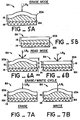
- Fig. 1 illustrates generally an erasable data storage medium 10 for storing data words in which each of the data words has a plurality of bits that are a logic 1 or a logic 0.
- the erasable data storage medium 10 can be an erasable optical data storage disc 12 which stores the data words over a plurality of concentric tracks T.
- the optical disc 12 also may be rotatable in the direction shown by the arrow for data recording purposes to be described below.
- Fig. 2 shows a section of a small bit area BA of the optical disc 12 for storing one data bit of logic 1 or logic 0.
- each bit area BA of the optical disc 12 includes a substrate 14 and a dual layer 16 deposited on the substrate 14.
- the dual layer 16 is susceptible to. expansion and relaxation, to writing data thermally (expansion), to erasing data thermally and mechanically (relaxation), and to reading data optically.
- Fig. 2 shows the dual layer 16 in a condition of relaxation corresponding to one logic state, e.g., logic 0, whereas Fig. 3 shows the dual layer 16 in the condition of expansion representing the other logic state, e.g., logic 1.
- the dual layer 16 has a bottom layer 18 of one material 18A and a top layer 20 of another material 20A. Neither the material 18A nor material 20A changes physical state upon expansion or relaxation of the dual layer 16.
- the material 18A and material 20A are bonded together at their interface 22, so as to, for example, erase a data bit at a high data rate, as will be further described.
- the material 18A is deposited on the substrate 14 such that at their interface 24, material 18A does not delaminate from substrate 14 upon expansion of the dual layer 16, as shown in Fig. 3. This substantially eliminates any "creep" of layer 18 about substrate 14, whereby the bit area BA will remain smooth over repeated erase/write cycles, as will be further described.
- material 18A and material 20A upon expansion of the dual layer 16, and as a result of the bonding at interface 22 and at interface 24, material 18A and material 20A will continue to be bonded together, while material 18A will still be in contact with, or not have delaminated from, substrate 14.
- Fig. 3 shows that the material 18A and the material 20A are deformed during expansion and, consequently, mechanical forces are produced in response to the expansion of the dual layer 16. As will be further described, these forces function, in part, to relax the dual layer 16 to the condition shown in Fig. 2 for purposes of quickly erasing a data bit.
- Material 18A has (1) low thermal conductivity, (2) a high coefficient of thermal expansion, (3) a glass transition temperature, Tg, considerably below the glass transition temperature of material 20A, below which material 18A is glassy. That is, in connection with property (3), the material 18A is rubbery at ambient temperature as opposed, for example, to being in a glassy or brittle condition. This means that only relatively low-power heating is required to heat the rubbery material, resulting in localized, extensive or large, and rapid expansion of the material 18A due to these three properties, respectively. Also as a result of this localized expansion, high data storage density can be achieved. Material 18A also may be relatively highly cross-linked, so that upon expansion there is substantially no viscous flow of this material. In addition, material 18A is elastic, having a high yield strain, so that upon being held in an extended state, it will not exceed its elastic limit. Other properties and characteristics of material 18A will be described below.
- Material 20A has (1) a glass transition temperature, Tg, considerably above that of material 18A for example 100°C, which is higher than ambient temperature. Thus, at ambient or normal temperatures material 20A is glassy or brittle, but when heated above the glass transition temperature, Tg, immediately transforms through a leathery or pliable condition into a rubbery condition. Material 20A also has (2) a relatively low thermal conductivity. Therefore, low-power heat can be used to quickly and locally, but only slightly, expand material 20A due to these properties.
- Tg glass transition temperature
- Material 20A may be either lightly cross-linked or depend upon chain entanglements to prevent excessive flow, and, may thus be either thermoplastic or thermoset with a relatively low yield strain. Therefore, upon expansion, the cross-linking or entanglements limits the viscous flow and a stretching of material 20A occurs.
- material 20A has a modulus of elasticity that varies with temperature. This modulus decreases with increasing temperature. This results in a reversible viscoelastic strain being induced very quickly at low light power, which holds the bump B, as shown in Fig. 3.
- Substrate 14 is a material that may, but not necessarily have, a low coefficient of thermal expansion.
- Layer 18 and layer 20 are optically coupled, so that substantially all the light that is propagated through layer 20 is absorbed in layer 18.
- This optical coupling is provided by the material 20A having about the same index of refraction as material 18A.
- substantially all this light can be coupled through top layer 20 to bottom layer 18, there is no loss of light, and therefore, low-power light sources can be used.
- Material 18A and material 20A are also capable of being optically tuned to any of a plurality of desired or given wavelengths of light.
- material 18A and material 20A can each constitute a light-transparent material that has added to it a dye or pigment to cause the respective material 18A and material 20A to absorb the given wavelength of light.
- material 18A and material 20A will be tuned to absorb different wavelengths of light with material 20A being substantially, but not entirely, transparent to the wavelength of light that can be absorbed by the material 18A.
- This optical tuning has the advantage of making the optical data storage medium 12 highly flexible in that it can be tuned to operate with a variety of different laser sources that are currently available and inexpensive or that might be available in the future.
- Fig. 4A-Fig. 4C illustrate a method for writing a data bit thermally at the bit area BA.
- the bit area BA of the erasable optical data storage medium 12 is in the relaxed condition described in connection with Fig. 2.
- material 18A may be above its glass transition temperature, Tg, and, therefore, rubbery
- material 20A is below its glass transition temperature, Tg, and, therefore, glassy.
- the material 18A and material 20A have the other properties and characteristics previously described, including for example, material 18A and material 20A being high yield strain and lower yield strain, respectively.
- the method includes heating the material 18A to expand the material 18A within its elastic limit.
- the material 20A also is heated above its glass transition temperature, Tg, which makes the material 20A rubbery.
- Tg glass transition temperature
- the heating of material 18A and material 20A is accomplished by generating a laser beam LB 1 that has a wavelength which is substantially transparent to the material 20A and absorptive by the material 18A, and focusing the laser beam LB 1 through the material 20A onto the material 18A.
- the light of the laser beam LB 1 may be slightly absorbed by the material 20A to produce the heat for making this material 20A rubbery and is substantially absorbed by material 18A for elastically expanding the material 18A onto the material 20A.
- the next step is allowing the heated material 18A to expand and push up the heated material 20A creating a deformation or bump, while the heated material 18A, expands.
- the next step shown in Fig. 4C, includes cooling the expanded material 20A below its glass transition temperature, Tg, while the material 18A is in the expanded condition. Upon cooling, the material 20A forms a reversibly fixed deformation or bump B and holds the material 18A in the expanded condition.
- a data bit of one logic level e.g., logic 1 has been written with the bit area BA being in the expanded condition described in connection with Fig. 3. If a logic 0 were to be written at the bit area BA, then laser beam LB 1 would not be actuated and the bit area BA would remain in the relaxed condition shown in Fig. 2.
- material 20A may absorb no such light. Rather, a small amount of the heat that is absorbed in material 18A is conducted or transferred to material 20A to heat the latter above its glass transition temperature, Tg.
- the method can include first heating the material 20A above its glass transition temperature, Tg, by generating a laser beam LB 2 shown in dotted lines and focusing the laser beam LB 2 on the material 20A.
- the laser beam LB 2 is of a wavelength that is substantailly absorbed by material 20A.
- the laser beam LB 1 is actuated and focused on the material 18A as described above, with the method for writing the data bit thermally continuing also as described above.
- One advantage to using the laser beam LB 2 initially is to more quickly bring the material 20A to a rubbery condition and, thereby, be able to write a data bit more quickly.
- Fig. 5A-Fig. 5C disclose the method for erasing a data bit thermally and mechanically.
- the bit area BA has a data bit written as illustrated in Fig. 5A, which shows the same expanded condition for the bit area BA as in Fig. 4C in which the material 20A is holding the material 18A in an expanded condition at ambient temperature.
- the method includes heating the material 20A to a temperature above the glass transition temperature, Tg, to make the material 20A rubbery. This heating of the material 20A, as shown in Fig. 5A, can be accomplished by generating and focusing the laser beam LB 2 onto material 20A.
- the heating of material 20A causes a relaxation of the holding by the material 20A of the material 18A, thereby allowing the mechanical forces previously mentioned to rapidly return the bit area BA to the relaxed condition shown in Fig. 4A.
- the elastic force in the material 18A assists in causing a quick return of the dual layer 16 to the relaxed condition.
- the material 20A and the overall dual layer 16 returns to the fully relaxed condition, and shown in Fig. 5B and as was described in connection with Fig. 2.
- the dual layer 16 upon cooling, returns to a smooth condition.
- the dual layer 16 has a relaxation time which is dependent, in part, on forces produced in response to the viscoelastic properties of the material 18A.
- Fig. 6A-Fig. 6B illustrates a method of reading a data bit optically.
- a data bit for example, a logic 1
- the laser beam LB which is at a lower power level than is used for writing or erasing the data bit
- the laser beam LB is generated and focused on the bump B of the material 20A.
- a data bit of logic 0 has been written in the bit area BA, as shown in Fig. 6B, i.e., no bump B is produced.
- the laser beam LB 1 at lower power level than is used for writing or erasing the data bit is generated and focused on the material 20A.
- the light of laser beam LB 2 will be reflected from the material 20A. Due to the difference in thickness or height H between the expanded condition of dual layer 16 shown in Fig. 6A and the relaxed condition of the dual layer 16 shown in Fig. 6B, there is a phase shift between the light of laser beam LB 1 that is reflected from the material 20A, respectively. This phase shift or difference can be detected with a high signal-to-noise ratio to distinguish a logic 1 from a logic 0 bit. Alternatively, there will be a difference in amplitude of the reflected light between the Fig. 6A and Fig. 6B conditions of bit area BA.
- This difference in amplitude can be detected with a high signal-to-noise ratio as logic 1 and logic 0 bits, respectively. More light scattering and, hence, reduced amplitude will be detected in the Fig. 6A condition than the Fig. 6B condition.
- Fig. 7A-Fig. 7B are used to explain an erase/ write cycle for erasing one data bit and writing another data bit at one bit area BA.
- the erase/write cycle occurs rapidly within the same view of an objective lens used to focus laser beam LB 1 and LB 2 on the material 18A and the material 20A, respectively, as the bit area BA moves across the lens.
- the erase/write cycle then includes first heating the material 20A at the bit area BA to erase the bit.
- the heating can be accomplished by generating and focusing the laser beam LB 2 on the material 20A to heat the material above its glass transition temperature, Tg, to a rubbery condition.
- another data bit e.g., a logic 1 is written at the bit area BA in the manner previously described for the Write Mode.
- This step of writing includes generating and focusing the laser beam LB 1 on the material 18A, as shown in Fig.
- the material 18A and the material 20A preferably are polymers, and particularly, amorphous polymers.
- the material 18A can be, for example, elastomers having the abovemen- tioned thermoelastic properties and characteristics.
- the elastomers can include butyl rubbers, silicone rubbers, natural rubbers, ethylene- copolymers, styrenebutadiene rubbers, and a number of other synthetic rubbers.
- the amorphous polymers of the material 20A are those having the thermosetting or thermoplastic properties with characteristics mentioned above. These may include, for example, cellulose acetate, cellulose acetate-butyrate, polystyrene, polysulfonamide, polycarbonate, cellulose nitrate, poly(ethyl-methacrylate), poly(vinyl butyral), aromatic polyester, polyamides and a wide variety of combinations thereof.
- amorphous polymers that can also be used include, for example, acrylic polymers, polyvinyl acetate, silicone resins, alkyd resins, styrene-butadiene copolymers, vinyl chloride-vinyl acetate copolymers, ethylcellulose, polyvinyl alcohol, and various other polymers.
- Other examples of dyes include those disclosed in U.S. Patent No. 3,689,768 at column 3, lines 1-22, and U.S. Patent No. 4,336,545 at column 8, lines 53-68, which patents are incorporated herein by reference for these dyes or pigments.
- Dow Corning 734 a clear silicone rubber, having a coefficient of thermal expansion of 920x10- 6 cm 3 /cm 3 /0°C, was mixed with a blue-green dye, Savinyl RLS Blue, manufactured by the Sandoz Corporation.
- the material 18A was then applied to the material 20A by using a "knife spread" technique. Then, the dual layer 16 was released or taken off the mandrel and mounted on a substrate 14 of aluminum.
- the fabricated substrate 14 and the dual layer 16 were then mounted in a "single-shot" laser system having a Krypton laser at a wavelength of 647 nanometers. Then, to write a data bit, the laser was actuated for 50 nanoseconds using an electro-optical crystal, with the laser light then propagated through a shutter, a 25 micron pinhole and a .45 N.A. objective lens which was anti-reflective coated. The laser power was at 820-880 milliwatts, with about 20-30% of this power being provided at the dual layer 16. Bumps B were created in the range of 2.5-5 microns in diameter.
- a "single-shot" erase system having an Argon laser at a wavelength of 488 nanometers was used.
- the laser beam was modulated using an acousto-optical modulator and was focused on bumps B through a microscope system using a 20x objective lens.
- the laser was operated at 1 microsecond pulse duration times and at 55 milliwatts of power, with about 11-12% of this power being applied at the dual layer 16.
- the bumps B were erased, as previously described.
- the data bits that were written on the fabricated substrate 14 and the dual layer 16 were read using white light and a microscope to project images of the bumps B on a glass plate. Then, using a fiber optic bundle hooked to a photomultiplier, the intensity of the light at the glass plate was detected. It was found that a satisfactory contrast ratio of about 2:1 to 3:1 existed between areas of the glass plate having the bumps B and areas of the glass plate having no bumps B.
- Fig. 8 illustrates one embodiment of a practical electro-optical system 26 for carrying out the optical recording of data on the erasable optical data storage medium 12.
- Fig. 8 shows one bit area BA, similar to the bit area BA shown in Fig. 2, for writing, reading and erasing a bit as described above.
- Electro-optical system 26 includes a digital data processing circuit 28 whose outputs on respective lines 30 and 32 control respective pulsed variable- intensity lasers 34 and 36.
- Laser 34 outputs the laser beam LB 2 and laser 36 outputs the laser beam LB 1 .
- a pair of lenses 38 and 40 collimate the laser beams LB 2 and LB,, respectively, which are then reflected by a mirror 42 and propagated through a beam splitter 44.
- the laser beam LB 2 and laser beam LB 1 are then passed through a filter 46 (e.g. waveplate) and then propagated through an objective lens 48 which focuses the laser beams on the moving bit area BA.
- a filter 46 e.g. waveplate
- an objective lens 48 which focuses the laser beams on the moving bit area BA.
- Light reflected by the material 20A of bit area BA is collected by the lens 48 and propagated through filter 46 to the beam splitter 44, where the reflected light is then propagated to a light sensor 50.
- laser beam LB 2 and laser beam LB 1 are spatially separated from one another. Also, the laser beam LB 2 is focused onto the bit area BA ahead of the laser beam LB 1 relative to the direction of movement of the bit area BA for erase/write purposes to be described below.
- the laser 34 is modulated by the output of the data processing circuit 28 on line 30 to produce a high intensity laser beam LB 2 .
- the laser beam LB 2 is then focused on the material 20A by lens 48 to heat it to a rubbery condition.
- the laser 36 is immediately modulated by the output of data processing circuit 28 over line 32 to produce the laser beam LB 1 . Consequently, the laser beam LB 1 is focused by the objective lens 48 onto the material 18A to heat it and cause the elastic expansion previously described.
- bit area BA will move out of the view of the objective lens 48 and cool, so that either a logic 1 or a logic 0 will be written.
- the erase/write cycle can occur within one bit cell time, which means within the same view of the objective lens 48.
- the data processing circuit 28, via line 30, modulates the laser 34 to output a high intensity laser beam LB 2 which is then focused on the material 20A. Therefore, the material 20A is heated and then cools as the bit area moves outside the view of the objective lens 48. The result is that the bit will be erased in the manner previously described.
- bit area BA which bit is either a logic 1 or a logic 0.
- the data processing circuit 28 modulates laser 34 to produce a low intensity laser beam LB 1 that is focused on the material 20A.
- the reflected light is then collected by lens 48 and propagated by filter 48 and beam splitter 44 to sensor 50 which then detects the logic state of the bit.
- differences in phase or amplitude of the reflected light can be detected by sensor 50 to distinguish a logic 1 from a logic 0.
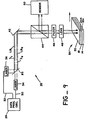
- Fig. 9 is similar to Fig. 8 except that rather than having spatially separated laser beams LB 1 and LB 2 , the two laser beams are concentric or co-linear.
- the co-linear beams LB 1 and LB 2 are propagated so that they are focused co-linearly on the material 18A and the material 20A as the bit area BA moves within the view of the objective lens 48.
- the co-linear laser beams LB 1 and LB 2 are produced by having laser 34 and laser 36 arranged, as shown, whereby light from each laser is propagated through a pollice beam splitter BS.
- the erase/write cycle, the erase cycle and the read cycle are performed in a similar manner in Fig. 9 as described in connection with Fig. 8.
Landscapes
- Optical Record Carriers And Manufacture Thereof (AREA)
- Optical Recording Or Reproduction (AREA)
- Thermal Transfer Or Thermal Recording In General (AREA)
Claims (30)
Priority Applications (1)
| Application Number | Priority Date | Filing Date | Title |
|---|---|---|---|
| AT84305735T ATE43739T1 (de) | 1983-08-22 | 1984-08-22 | Loeschbares medium fuer optische datenspeicherung und verfahren zur aufzeichnung von daten auf dem medium. |
Applications Claiming Priority (2)
| Application Number | Priority Date | Filing Date | Title |
|---|---|---|---|
| US52581383A | 1983-08-22 | 1983-08-22 | |
| US525813 | 1983-08-22 |
Publications (2)
| Publication Number | Publication Date |
|---|---|
| EP0136070A1 EP0136070A1 (de) | 1985-04-03 |
| EP0136070B1 true EP0136070B1 (de) | 1989-05-31 |
Family
ID=24094710
Family Applications (1)
| Application Number | Title | Priority Date | Filing Date |
|---|---|---|---|
| EP84305735A Expired EP0136070B1 (de) | 1983-08-22 | 1984-08-22 | Löschbares Medium für optische Datenspeicherung und Verfahren zur Aufzeichnung von Daten auf dem Medium |
Country Status (5)
| Country | Link |
|---|---|
| EP (1) | EP0136070B1 (de) |
| JP (1) | JPH07118090B2 (de) |
| AT (1) | ATE43739T1 (de) |
| CA (1) | CA1229410A (de) |
| DE (1) | DE3478528D1 (de) |
Families Citing this family (33)
| Publication number | Priority date | Publication date | Assignee | Title |
|---|---|---|---|---|
| US4780867A (en) * | 1986-10-02 | 1988-10-25 | Optical Data, Inc. | Method for erasably recording data by viscoelastic shear deformation |
| US4901304A (en) * | 1986-10-08 | 1990-02-13 | Optical Data, Inc. | Erasable optical data storage medium having a zoned integral recording layer |
| US4825430A (en) * | 1986-12-19 | 1989-04-25 | Optical Data, Inc. | Erasable optical data storage medium having an embedded servo track and a subsurface recording interface |
| EP0320834A3 (en) * | 1987-12-14 | 1990-11-14 | E.I. Du Pont De Nemours And Company | Optical recording medium |
| US5214632A (en) * | 1987-12-23 | 1993-05-25 | U.S. Philips Corporation | Method of manufacturing a matrix and a master plate suitable for use in the method |
| US5001035A (en) * | 1988-01-06 | 1991-03-19 | U.S. Philips Corporation | Method of recording information, recording element manufactured according to the method and method of producing a metal matrix |
| US4879709A (en) * | 1988-02-05 | 1989-11-07 | Tandy Corporation | Dye-polymer optical data storage media with improved recording sensitivity |
| US5016239A (en) * | 1988-02-05 | 1991-05-14 | Tandy Corporation | Recording method and apparatus |
| US5036511A (en) * | 1988-02-05 | 1991-07-30 | Tandy Corporation | Recording method and apparatus |
| US5001699A (en) * | 1988-02-05 | 1991-03-19 | Tandy Corporation | Recording method and apparatus |
| US5088088A (en) * | 1988-02-05 | 1992-02-11 | Tandy Corporation | Dye-polymer optical data storage media with improved recording sensitivity |
| US5200948A (en) * | 1988-02-05 | 1993-04-06 | Tandy Corporation | Recording method and apparatus |
| US5090008A (en) * | 1988-02-05 | 1992-02-18 | Tandy Corporation | Erasable recording media |
| US5208801A (en) * | 1988-02-05 | 1993-05-04 | Tandy Corporation | Method and apparatus for correcting focus in an optical recording system |
| US5014259A (en) * | 1988-02-05 | 1991-05-07 | Tandy Corporation | Recording medium having an insulating layer |
| US4918682A (en) * | 1988-02-05 | 1990-04-17 | Tandy Corporation | Ablative and bump-forming optical recording media including a metallic reflective layer |
| US5018128A (en) * | 1988-02-05 | 1991-05-21 | Tandy Corporation | Apparatus and medium for recording erasable information |
| US4852077A (en) * | 1988-02-05 | 1989-07-25 | Tandy Corporation | Optical data storage media with spatially variable energy absorptivity |
| EP0328212A1 (de) * | 1988-02-11 | 1989-08-16 | Koninklijke Philips Electronics N.V. | Verfahren zum Herstellen einer Metallmatrize und Mutterplatte zum Herstellen von Matrizen |
| US4896314A (en) * | 1988-04-19 | 1990-01-23 | Optical Data, Inc. | Bump-forming media including thin intermediate reflective layer and methods for writing, reading, and erasing same |
| US5215800A (en) * | 1989-01-17 | 1993-06-01 | Teijin Limited | Erasable optical recording medium and method for writing, reading and/or erasing thereof |
| JP2771231B2 (ja) * | 1989-03-27 | 1998-07-02 | 帝人株式会社 | 消去可能な光学情報記録媒体および情報の記録・消去方法 |
| EP0379276B1 (de) * | 1989-01-17 | 1994-11-30 | Teijin Limited | Auswischbares optisches Aufzeichnungsmedium und Verfahren zum Schreiben, Lesen und/oder Auswischen in diesem Medium |
| US5175720A (en) * | 1989-05-25 | 1992-12-29 | Tandy Corporation | Interactive optical disk |
| US5079758A (en) * | 1989-09-28 | 1992-01-07 | Tandy Corporation | Single polymer layer recordable/erasable optical media |
| US5118541A (en) * | 1989-06-19 | 1992-06-02 | Matsushita Electric Industrial Co., Ltd. | Erasable optical disk media and method of recording/erasing the same |
| MY105728A (en) * | 1989-06-30 | 1994-11-30 | Phillips And Du Pont Optical Company | Direct effect master/stamper for optical recording |
| CA2026758A1 (en) * | 1989-10-03 | 1991-04-04 | Takeyuki Kawaguchi | Optical data storage medium formed of uv-curable resin and process for the production thereof |
| US5144613A (en) * | 1990-07-26 | 1992-09-01 | Tandy Corporation | Thermal bulk erasure method for dye polymer optical media |
| US5406544A (en) * | 1991-07-25 | 1995-04-11 | Clark; Bryan K. | Low cost substrate for bump-forming recording media |
| JP5553723B2 (ja) | 2010-10-19 | 2014-07-16 | 富士フイルム株式会社 | 光情報記録媒体 |
| JPWO2014050443A1 (ja) | 2012-09-27 | 2016-08-22 | 富士フイルム株式会社 | 光情報記録媒体およびその製造方法 |
| WO2014136486A1 (ja) | 2013-03-08 | 2014-09-12 | 富士フイルム株式会社 | 光情報記録媒体 |
Family Cites Families (6)
| Publication number | Priority date | Publication date | Assignee | Title |
|---|---|---|---|---|
| JPS5528530A (en) * | 1978-08-17 | 1980-02-29 | Matsushita Electric Ind Co Ltd | Optical information recording method |
| US4264986A (en) * | 1979-03-12 | 1981-04-28 | Willis Craig I | Information-recording process & apparatus |
| US4300227A (en) * | 1979-10-17 | 1981-11-10 | Rca Corporation | Replicable optical recording medium |
| FR2475270A1 (fr) * | 1980-02-01 | 1981-08-07 | Thomson Csf | Structure de memoire reversible, a inscription thermo-optique et lecture optique, et procede d'inscription et d'effacement de cette structure |
| JPS5871194A (ja) * | 1981-10-23 | 1983-04-27 | Toshiba Corp | 情報記録再生方法 |
| CA1192662A (en) * | 1982-06-21 | 1985-08-27 | James E. Kuder | Erasable recording medium comprising a dimer acid polyamide resin |
-
1984
- 1984-06-28 JP JP59132116A patent/JPH07118090B2/ja not_active Expired - Lifetime
- 1984-07-18 CA CA000459199A patent/CA1229410A/en not_active Expired
- 1984-08-22 EP EP84305735A patent/EP0136070B1/de not_active Expired
- 1984-08-22 DE DE8484305735T patent/DE3478528D1/de not_active Expired
- 1984-08-22 AT AT84305735T patent/ATE43739T1/de not_active IP Right Cessation
Also Published As
| Publication number | Publication date |
|---|---|
| JPS6069846A (ja) | 1985-04-20 |
| CA1229410A (en) | 1987-11-17 |
| ATE43739T1 (de) | 1989-06-15 |
| JPH07118090B2 (ja) | 1995-12-18 |
| EP0136070A1 (de) | 1985-04-03 |
| DE3478528D1 (en) | 1989-07-06 |
Similar Documents
| Publication | Publication Date | Title |
|---|---|---|
| EP0136070B1 (de) | Löschbares Medium für optische Datenspeicherung und Verfahren zur Aufzeichnung von Daten auf dem Medium | |
| US4719615A (en) | Erasable optical data storage medium | |
| US4852075A (en) | Erasable optical data storage medium and method and apparatus for recording data on the medium | |
| US4825430A (en) | Erasable optical data storage medium having an embedded servo track and a subsurface recording interface | |
| US4912696A (en) | Erasable optical data storage medium and method and apparatus for recording data on the medium | |
| JP2797733B2 (ja) | 光学情報記録部材の記録方法 | |
| EP0338776B1 (de) | Beulenformende Medien mit zwischenliegender, reflektierender Dünnschicht und Methoden zum Aufschreiben auf, Auslesen und Auslöschen aus derselben | |
| JPS63136337A (ja) | データ書込方法及びこの方法の実施に使用する可消去光学データ蓄積媒体 | |
| JPH02504565A (ja) | 立体変化可能なエネルギ吸収性を有する光学データ記憶媒体 | |
| US4879709A (en) | Dye-polymer optical data storage media with improved recording sensitivity | |
| WO1989007311A1 (en) | Optical media reflective materials | |
| GB2055218A (en) | Optical recording member | |
| US5200948A (en) | Recording method and apparatus | |
| US5079758A (en) | Single polymer layer recordable/erasable optical media | |
| KR900006306B1 (ko) | 소거 가능한 광학식 데이터 저장매체 및 그 매체에 데이터를 기록하기 위한 방법 및 장치 | |
| KR100247792B1 (ko) | 유기광기록 테이프 | |
| EP0320834A2 (de) | Optischer Aufzeichnungsträger | |
| EP0473709A1 (de) | Wechselwirkende optische scheibe und systeme und methoden zur verwendung dergleichen | |
| JP2705330B2 (ja) | 光記録媒体 | |
| WO1991016707A1 (en) | Method and apparatus for correcting focus in an optical recording system | |
| KR100207581B1 (ko) | 광기록매체 | |
| EP0473672A1 (de) | Wechselwirkende optische scheibe, verfahren zur herstellung dergleiche und gerät zur aufzeichnung darauf | |
| KR100247793B1 (ko) | 유기광기록 테이프 | |
| KR100204350B1 (ko) | 유기광기록 테이프 | |
| JPS62116190A (ja) | 記録装置 |
Legal Events
| Date | Code | Title | Description |
|---|---|---|---|
| PUAI | Public reference made under article 153(3) epc to a published international application that has entered the european phase |
Free format text: ORIGINAL CODE: 0009012 |
|
| AK | Designated contracting states |
Designated state(s): AT BE CH DE FR GB IT LI NL SE |
|
| 17P | Request for examination filed |
Effective date: 19850615 |
|
| 17Q | First examination report despatched |
Effective date: 19860828 |
|
| GRAA | (expected) grant |
Free format text: ORIGINAL CODE: 0009210 |
|
| RAP3 | Party data changed (applicant data changed or rights of an application transferred) |
Owner name: OPTICAL DATA, INC. |
|
| AK | Designated contracting states |
Kind code of ref document: B1 Designated state(s): AT BE CH DE FR GB IT LI NL SE |
|
| REF | Corresponds to: |
Ref document number: 43739 Country of ref document: AT Date of ref document: 19890615 Kind code of ref document: T |
|
| REF | Corresponds to: |
Ref document number: 3478528 Country of ref document: DE Date of ref document: 19890706 |
|
| ITF | It: translation for a ep patent filed | ||
| ET | Fr: translation filed | ||
| PLBE | No opposition filed within time limit |
Free format text: ORIGINAL CODE: 0009261 |
|
| STAA | Information on the status of an ep patent application or granted ep patent |
Free format text: STATUS: NO OPPOSITION FILED WITHIN TIME LIMIT |
|
| 26N | No opposition filed | ||
| PGFP | Annual fee paid to national office [announced via postgrant information from national office to epo] |
Ref country code: SE Payment date: 19910617 Year of fee payment: 8 |
|
| PGFP | Annual fee paid to national office [announced via postgrant information from national office to epo] |
Ref country code: AT Payment date: 19910701 Year of fee payment: 8 |
|
| PGFP | Annual fee paid to national office [announced via postgrant information from national office to epo] |
Ref country code: BE Payment date: 19910715 Year of fee payment: 8 |
|
| PGFP | Annual fee paid to national office [announced via postgrant information from national office to epo] |
Ref country code: CH Payment date: 19911231 Year of fee payment: 8 |
|
| PG25 | Lapsed in a contracting state [announced via postgrant information from national office to epo] |
Ref country code: AT Effective date: 19920822 |
|
| PG25 | Lapsed in a contracting state [announced via postgrant information from national office to epo] |
Ref country code: SE Effective date: 19920823 |
|
| PG25 | Lapsed in a contracting state [announced via postgrant information from national office to epo] |
Ref country code: LI Effective date: 19920831 Ref country code: CH Effective date: 19920831 Ref country code: BE Effective date: 19920831 |
|
| BERE | Be: lapsed |
Owner name: OPTICAL DATA INC. Effective date: 19920831 |
|
| REG | Reference to a national code |
Ref country code: CH Ref legal event code: PL |
|
| ITTA | It: last paid annual fee | ||
| PGFP | Annual fee paid to national office [announced via postgrant information from national office to epo] |
Ref country code: NL Payment date: 19940831 Year of fee payment: 11 |
|
| EUG | Se: european patent has lapsed |
Ref document number: 84305735.7 Effective date: 19930307 |
|
| PG25 | Lapsed in a contracting state [announced via postgrant information from national office to epo] |
Ref country code: NL Effective date: 19960301 |
|
| NLV4 | Nl: lapsed or anulled due to non-payment of the annual fee |
Effective date: 19960301 |
|
| PGFP | Annual fee paid to national office [announced via postgrant information from national office to epo] |
Ref country code: GB Payment date: 19980804 Year of fee payment: 15 |
|
| PGFP | Annual fee paid to national office [announced via postgrant information from national office to epo] |
Ref country code: FR Payment date: 19980818 Year of fee payment: 15 |
|
| PGFP | Annual fee paid to national office [announced via postgrant information from national office to epo] |
Ref country code: DE Payment date: 19981022 Year of fee payment: 15 |
|
| PG25 | Lapsed in a contracting state [announced via postgrant information from national office to epo] |
Ref country code: GB Free format text: LAPSE BECAUSE OF NON-PAYMENT OF DUE FEES Effective date: 19990822 |
|
| GBPC | Gb: european patent ceased through non-payment of renewal fee |
Effective date: 19990822 |
|
| PG25 | Lapsed in a contracting state [announced via postgrant information from national office to epo] |
Ref country code: FR Free format text: LAPSE BECAUSE OF NON-PAYMENT OF DUE FEES Effective date: 20000428 |
|
| PG25 | Lapsed in a contracting state [announced via postgrant information from national office to epo] |
Ref country code: DE Free format text: LAPSE BECAUSE OF NON-PAYMENT OF DUE FEES Effective date: 20000601 |
|
| REG | Reference to a national code |
Ref country code: FR Ref legal event code: ST |